1. Introduction
Group III nitrides, including (Al, In, Ga)N compounds, gained importance at the turn of the 20th and 21st centuries, especially in the field of optoelectronics and high power electronics. Gallium nitride is characterised by a wide band gap (3.4 eV) [
1], high chemical and temperature stability [
2] and large piezoelectric coefficients [
3]. Its unique properties make it a material of choice for many advanced semiconductor devices, such as: high temperature devices, high electron mobility transistors (HEMT), microwave instruments, facet lasers, electroacoustic transducers and electromechanical resonators, field emitters or integrated optics devices. Those devices consist of 3D structures, such as U-shaped and V-shaped grooves, mesa structures, nanowire matrices or planar waveguides, which can be produced in two ways. In top-down architecture, the epitaxial layer is spatially patterned by wet or dry chemical etching, whereas, in bottom-up architecture, structures are selectively grown while using dielectric masks. Because of this, it is possible to integrate many opto-electro-mechanical devices within one semiconductor substrate, which is required in order to achieve compactness, high stability, and efficiency, as well as minimise losses in modern, technologically advanced semiconductor devices [
4].
Metalorganic vapour-phase epitaxy (MOVPE) is the most popular method that is used industrially to produce high quality gallium nitride layers. The possibility of precise control of several process parameters allows for the fabrication of sophisticated planar nano- and microstructures. The use of SA-MOVPE to get 3D semiconductor epitaxial growth on the nano- and micro scale is a promising, but challenging, approach. Numerous factors have to be addressed in the technological process. First of all, conducting epitaxy on a masked substrate causes heterogeneous layer growth in the window area. This phenomenon is called the edge effect and it results from excessive accumulation of epitaxial material adjacent to the dielectric mask. This is also associated with a different growth rate of a structure relative to non-selective deposition [
4]. Homogeneous structure growth along the window area is necessary for keeping continuous metallization for the contact layer and close fitting between semiconductor components.
Two mechanisms of mass transport into the window area could be distinguished during the MOVPE process: vapour-phase diffusion and surface diffusion. The diffusion length of precursor molecules in vapour is several orders of magnitude greater than the surface diffusion length of the adatoms [
5]. It was proved, for the first time, by Gibbon regarding InP selective deposition [
6]. Mass diffusion is caused by precursor concentration gradient between masked and unmasked substrate surface. The Laplace Equation (
1) describes the precursor concentration
in the steady state
The mass flux to the substrate surface is balanced by molecule incorporation into grown layer, as local thermodynamic equilibrium can be established in the vicinity of the growth interface [
7]. This can be formulated by a combination of Fick’s first law and Langmuir adsorption model (
2) [
6]
where
D is diffusion coefficient,
k is surface reaction rate, and
refers to the normal vector. Assuming that no crystal growth occurs on the dielectric mask, the reaction rate on masked substrate is equal to zero (
3)
The ratio
is the key factor influencing the shape of the structure profile in the window area. It used to be called the effective lateral diffusion length of precursor molecules
[
4,
8,
9,
10]. Molecules are incorporated with similar probability into the epitaxial structure within the whole window area when the effective diffusion length is greater than the half-width of the window. Otherwise, the uneven accumulation of epitaxial material will be observed [
4,
5,
6,
8,
9,
10,
11,
12,
13,
14,
15,
16,
17,
18]. Surface diffusion additionally influences structure shape adjacent to the mask. The overall participation of surface diffusion in the profile of an epitaxial structure increases with the thickness of the deposited layer [
14,
19]. The diffusion length is strongly dependent on the composition and material parameters of the precursors in the reactor chamber, as well as the carrier gas type [
5] and process parameters, such as pressure or temperature [
4]. The effective diffusion length is primarily affected by the group III precursors concentration, as group V molecules have a minor influence on the growth rate [
20].
A crucial aspect of the selective area epitaxy (SAE) of AlGaN/GaN heterostructures is a horizontal gradient of the Al
xGa
1-xN composition that is caused by the difference in the diffusion lengths of Al and Ga molecules. Compositional variation is primarily derived by vapour-phase diffusion [
9,
19]. Based on Lennard–Jones potential theory, diffusion length is assumed to be inversely proportional to the square of the Lennard–Jones theorem length σ [
4]. The effective diffusion length of Al molecules is expected to be smaller than the effective diffusion length of Ga molecules when using TMAl (trimethylaluminium) and TMGa (trimethylgallium) as precursors for AlGaN deposition, as σ is longer in TMAl than in TMGa [
21]. This leads to a larger concentration of Al adjacent to the mask when compared to the window center. Precise control of compositional variation is substantial for the fabrication of highly efficient optoelectronic devices while using multiple quantum wells (MQWs), as the application of MQWs causes a decrease of carrier lifetime and an increase of radiative recombination efficiency [
15,
19]. On the other hand, compositional uniformity is required in the heterojunction band-gap engineering for the application of HEMT or planar waveguides.
There were researches that were conducted for both rectangular [
5,
6,
8,
9,
10,
15,
16] and hexagonal windows in the mask [
11,
12,
13,
22]. All of them showed that the edge effect is strongly dependent on the structure geometry and configuration of the dielectric mask. According to Hara, the profile of selectively grown layer can be described as (
4) [
16]
where
refers to layer thickness at the distance
x from the mask edge,
is the layer thickness adjacent to the mask, and
indicates the thickness of the non-selectively deposited epitaxial layer under the same growth conditions. Equation (
4) allows for the calculation of the effective diffusion length based on the measurements of the epitaxial material agglomeration in windows in the dielectric mask. By dividing both sides of Equation (
4) by
, an equation describing growth rate enhancement (GRE) at the distance
x from the mask edge is obtained:
In order to maximize the GRE value difference, window half-width as the distance from the mask edge was chosen:
The effective diffusion length
can be then calculated by
where
The effective diffusion length has been estimated so far either by calculation while using the Hara Equation (
4) [
10,
16,
18] or by fitting mathematical models to the experimental data (simulations) [
4,
5,
6,
8,
9,
11,
14,
17]. Published research overwhelmingly focused on the selective epitaxy of GaAs and its ternary compounds. This paper presents a new method for the estimation of the precursor molecules diffusion length according to the relative height difference between the edge and center of the grown heterostructure.
2. Materials and Methods
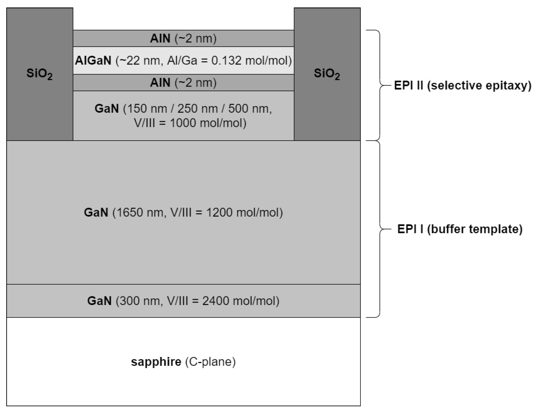
The test structures were deposited on GaN/sapphire templates while using an AIXTRON CCS
epitaxial system.
Figure 1 shows the layers scheme of the investigated structures. An undoped GaN buffer layer with a total thickness of 1950 nm was grown prior to selective epitaxy. Trimethylgallium (TMGa) and ammonia (NH
3) with different molar ratios were used as precursors for GaN growth with H
2 as a carrier gas. Next, a 400 nm thick SiO
2 mask was deposited by PECVD (plasma enhanced chemical vapour deposition), followed by UV photolithography. The selective epitaxy of AlGaN/GaN heterostructures with AlN cladding and cap layers was conducted at 1060
and pressure of 10 kPa with NH
3 flow of 67 mmol·min
−1, and TMGa and TMAl flow of 65 μmol·min
−1 and 8.6 μmol·min
−1, respectively. The selected conditions ensured that the epitaxial layer was deposited in the mass-transport limited growth regime [
23]. Three samples differing in GaN thickness (150 nm, 250 nm, and 500 nm) were successfully fabricated. Epitaxial lateral overgrowth was not observed.
Figure 2 presents the configuration of the SiO
2 mask. Selective epitaxy was conducted in windows of different width
w (from 5 μm to 160 μm) and length of 200 μm. The distance between windows (mask width
m) varied from 5 μm to 40 μm. The rectangular heterostructure deposited selectively between two dielectric masks could be used as the active region of a high electron mobility transistor [
24].
The measurements of the epitaxial material agglomeration in windows in the dielectric mask were conducted while using Taylor Hobson Talysurf CCI optical profilometer. Coherence correlation interferometry was used as a measurement technique with 0.01 nm vertical and 0.6 μm lateral resolution. The layers profile has been determined after the removal of the dielectric mask. The whole structure was covered with a 10 nm layer of gold in order to increase the measurement accuracy. This caused an increase in the reflection coefficient and reduction of the optical beam interference on the heterostructure. Additional measurements were performed while using Bruker Multimode V Atomic Force Microscope for measurements accuracy comparison. The data presented in this study are available in the
Supplementary Materials. Measurement data have been divided into three sets depending on the thickness of the GaN layer (150 nm, 250 nm and 500 nm).
3. Results and Discussion
Figure 3 shows a part of the AlGaN/GaN heterostructure profile with the 500 nm thick GaN layer. The abscissa axis shows the profile width, whereas the ordinate axis shows the profile height relative to the GaN buffer layer surface. Increased material accumulation adjacent to the dielectric mask was observed. Fluctuations in the material growth rate at the mask edge were evaluated in dependence of the surface of the masked and exposed area, based on the obtained profiles. The overall layer profile was assembled of fragments that were measured separately. A separate calibration of the structure height reference point was conducted for each part. This resulted in a nonuniform buffer surface layer level that is visible in
Figure 3. Additionally, the substrate deformed due to stresses that arose in the deposited layer.
The following parameters were calculated for each window separately (
Figure 4) in order to eliminate measurement errors that result from substrate deformation:
average structure height adjacent to the mask as a mean of structure height relative to the bottom of the mask on the left and right side of the structure;
average structure height at the window center as a mean of structure height relative to the bottom of the mask on the left and right side of the structure;
window width w;
average mask width m as a mean of mask width on the left and right side of the window; and,
edge growth factor σ as a relative height difference between
and
(
9).
A detailed analysis of the measured profile was conducted for the sample with a 500 nm thick GaN layer.
Figure 5 (variable window width) and
Figure 6 (variable mask width) present growth rate enhancement as a function of location relative to the window center. The presented results are cross-sections of selected test structures.
Figure 5 shows that, with increasing window width, for a constant mask width and layer thickness, the height of the epitaxial structure decreases significantly and the edge growth factor increases. The average structure height at the window center for a 5 μm wide window is almost twice as large as for a 160 μm wide window. The shape of the profile is similar for different window widths. When reducing the size of the window, the structure edges are brought closer, without a significant change in the shape of the profile. For narrow windows (
μm), structure edges overlap, which results in a nearly uniform layer surface.
Figure 6 shows that, with increasing mask width, for a constant window width and layer thickness, the height of the epitaxial structure increases with a slight change in the shape of the profile.
The GRE of the epitaxial structure as a function of window width is presented in
Figure 7 (adjacent to the mask) and in
Figure 8 (in the window center). GRE decreases exponentially with increasing windows width. This agrees with previous findings by Tanaka [
11], and it can be easily understood, as the same amount of material has to be deposited on a larger area. The vertical dimensions of the layer are also affected by the surrounding mask width. The structure height increases with increasing mask width. All of the approximation curves were fitted to the measurement data while using orthogonal distance regression method with the value of the adjusted R-squared over 0.99.
The relation between GRE and window width can be expressed as (
10)
where
refers to the minimal growth rate enhancement for a window width much greater than the effective diffusion length (
), and
is the excess growth rate enhancement dependent on the window width. The effective diffusion length
defines the steepness of the relation between the GRE and the window width. Greater
means that the epitaxial material diffusing from the mask will be distributed over a larger area.
Table 1 depics the values of
,
, and
for different mask widths. Error margins have been estimated as the statistical error of the orthogonal distance regression method.
The sensitivity matrix
X (
11) has been calculated in order to analyse the influence of the parameters
,
, and
on the absolute growth rate enhancement
where
is a vector of parameters:
,
, and
. The values of sensitivity to particular parameters may vary significantly, thus the dimensionless normalized sensitivity matrix
(
12) was calculated by the multiplication of sensitivity matrix
and normalization diagonal matrix
Matrix
satisfies the Equation (
13)
where
is the identity matrix and ∘ denotes the Hadamard product. Normalized sensitivity to
,
, and
as a function of window width, for a constant mask width
μm, is presented in
Figure 9. GRE at the window edge was considered. The value of
is independent of window width and it has a dominant influence on growth rate enhancement for windows that are much broader than the effective diffusion length (
) (
14)
Window center will not be affected by lateral diffusion provided that , thus at the window center.
Excess growth rate enhancement
has the greatest impact on absolute GRE for windows that are narrower than effective diffusion length. It is related to the constant amount of material that has to be deposited on a variable surface area. Reducing window width leads to higher GRE, as the same amount of epitaxial material has to be deposited on a smaller area (
15)
Effective diffusion length influences GRE the most for a window width equal to .
Figure 10 presents the
ratio as a function of window width. For windows that are narrower than 20 μm,
is equal to one. This indicates uniform growth within the whole window area, as the structure height at the window edge is equal to the structure height at the window center. Because of this, Hara Equation (
4) cannot be used for estimating the effective diffusion length in this range (
). For wide windows,
approaches zero. It means that layer at the window center is equal in height to the layer deposited non-selectively, thus window center was not affected by mass diffusing from the dielectric mask.
Figure 11 presents the effective diffusion length that was calculated using the Hara Equation (
4) for different window and mask widths. Window widths that were smaller than 20 μm were not included. It can be easily seen that
calculated while using Equation (
4) depends on both window and mask width. Effective diffusion length decreases exponentially with an increasing window width. Offset values for different mask widths are within error margin of
estimated while using Equation (
10) at the window edge, thus Equation (
10) is coherent with Equation (
4) and Equation (
4) should be used only to windows that are much wider than the exact value of the effective diffusion length (here:
).
Table 1 illustrates the offset values. For similar process conditions,
of about 30 μm has been reported [
4,
11,
25]. It is expected that the effective diffusion length will decrease with decreasing temperature [
4,
9,
19,
25] and increasing pressure [
4,
5,
9,
19,
25]. Similarly, an increase in the temperature causes an increase in the effective diffusion length [
4,
8,
25]. Therefore, the calculated values of the effective diffusion length are in agreement with previous reports.
Figure 12 presents the effective diffusion length that was calculated using Equation (
10) at the window edge and center as a function of the mask width. Both of the relations are linear and they share the same intercept equal to 15 μm that can be interpreted as the lateral vapour diffusion length of Ga
, independent of the mask configuration and structure geometry. Slopes of approximation lines are equal to 0.5 μm
−1 and 0.3 μm
−1 for the window center and window edge, respectively. Therefore, Equation (
10) can be transformed into Equations (
16) and (
17).
Figure 13 presents the edge growth factor as a function of window width. It can be seen that the larger the window width and the greater the distance between windows, the greater the difference in structure height between the edge and the window center. This effect is also visible in
Figure 3, showing the layer altitude profile. An increased agglomeration of epitaxial material adjacent to the mask may not be observed for narrow windows, while more intense layer growth will be seen throughout the entire window area. This increase will be faster for smaller window area and larger mask area.
Uniform layer growth will be observed, provided that the distance between the mask center and window center will be smaller than the effective diffusion length (
18)
When considering Equation (
17), this condition can be expressed as
Figure 13 marks a value of
. It can be seen that, for a window width smaller than
, nearly uniform layer growth was observed. In order to compare measurement accuracy, a heterostructure with a 250 nm thick GaN layer was additionally profiled while using atomic force microscope (AFM). Edge growth factor as a function of window width calculated using different profiling methods is presented in
Figure 14. Optical profilometer and AFM both have similar accuracy regarding window widths satisfying the condition (
19).
GRE as a function of location relative to the window center for a constant window and mask width and different nominal GaN layer thickness is presented in
Figure 15.
Figure 16 presents the edge growth factor as a function of the mask surface to the window surface ratio for three different GaN layer thicknesses.
Figure 15 and
Figure 16 suggest that GRE is independent of the structure thickness, thus growth uniformity cannot be achieved by the modification of the deposition time or the mask configuration. The edge growth factor can be minimised by selection of the sufficiently narrow dielectric mask, but uniform front of crystallization for a constant window width can only be achieved by modification of the diffusion length of precursor molecules. This can be achieved by a variation of the process parameters, such as temperature or pressure [
4].

 ,
, 


