Abstract
With the decreasing size of manufacturing process, the scale of island-style field programmable gate array (FPGA) becomes larger, which leads to the increasing complexity of FPGA routing resources, especially hex programmable interconnect points (PIPs). Hex PIPs which span six tiles of the island-style FPGA have complex interconnect rules. Accordingly, research on complete hex PIPs test is rarely involved in the study of routing resources test. Therefore, this paper analyzes the hex PIPs architecture of the island-style FPGA, summarizes the interconnect rules of the hex PIPs mathematically in a two-dimensional coordinate system, and presents two proper test algorithms at the same time. The hex PIPs are divided into three directions, that is, horizontal, vertical, and oblique. According to the proposed coordinate equations, a cycle test structure in the horizontal and vertical directions and a test structure with partial-cascade patterns in the oblique direction are designed respectively. It is concluded that the proposed methods can achieve 100% fault coverage for the hex PIPs test in all directions, and the configuration number for hex lines test with the same methods is significantly decreased than previous researches.
1. Introduction
Field programmable gate array (FPGA) has been widely used in product design and prototype design [1,2]. The advantages of FPGA including high performance, fast time-to-market, low cost, long-term maintenance, design flexibility, and so forth. With the continuous improvement of FPGA performance and cost-effectiveness, there are more and more products based on FPGA [3]. Routing resources, also called interconnect resources, are the principal programmable resources of the island-style FPGA. The configuration bits of the routing resources usually account for more than 80% of the total configuration memory bits of the island-style FPGA. Furthermore, this number goes up to 90% in some modern FPGAs, and the area of the routing resources covers more than that of the logic resources [4].
Routing resources include single lines, single programmable interconnect points (PIPs), double lines, double PIPs, hex lines, hex PIPs, and so forth. Early studies for routing resources performed the test pattern generator (TPG) and the output response analyzer (ORA) externally [5,6]. With the characteristic of rapid hardware diagnosis, build-in self-test (BIST) was gradually used to test single lines [7]. It implemented the TPG and the ORA by configurable logic block (CLB) resources, thus greatly reducing the consumption of I/O resources [8,9,10,11,12]. Sun et al. [8] proposed a parity-based BIST approach for Xilinx 4000 series FPGAs. It required six configurations to complete the test of single lines. Tahoori [13] proposed a research on single lines and single PIPs with MAX Flow algorithm, whereas Bai et al. [14] extended the application of the MAX Flow algorithm to Virtex5 for double lines test with huge number of configurations. Zhao et al. [15] tested single lines and single PIPs separately with improved depth first search (DFS) algorithm. The test was completed with 16 configurations, which was fewer than the number of the configurations in Tahoori [13]. For double lines test, an effective method was proposed in Dixon [16], in which the test was completed with 17 configurations in both horizontal and vertical directions. For more complex hex lines test, YAO [17] proposed a solution in which the number of configurations in the horizontal direction and the vertical direction were eight and 16, respectively. However, both methods shown in Dixon [16] and YAO [17] ignored the PIPs test in the oblique direction. Banik [18,19] proposed an application-dependent test scheme which has low test coverage because it only tests the used interconnect resources. In addition, Ruan [20,21] proposed a method for all interconnect resource test based on graph theory algorithms but with more configuration times. Briefly speaking, the test for the complete hex PIPs is rarely involved in researches on routing resource test except Ruan [20,21].
This paper focuses on the solution for the hex PIPs test of the island-style FPGA. The fault model in this paper is open fault of PIPs and interconnected lines, which can be represented as stuck-at 0 and stuck-at 1. The main contributions of this paper are three-fold:
- An analytical model with several coordinate equations is established to evaluate the propagation of the hex lines. The proposed model can be used to summarize the interconnect rules of the hex PIPs.
- Two coordinate methods for design of high coverage test patterns with corresponding test algorithms are presented.
- In addition to the hex PIPs test, the hex lines test is also covered without any additional effort. Moreover, compared with YAO [17], the configuration number required for the hex lines test is reduced from 24 to four.
The rest of the paper is organized as follows. Preliminaries and background are provided in Section 2. Section 3 describes the analytical model in a two-dimensional coordinate system. Section 4 presents the coordinate methods for hex PIPs test. Then, test algorithms and experimental results are given in Section 5. Finally, conclusions are drawn in Section 6.
2. Preliminaries and Background
A typical island-style FPGA consists of an array of logic blocks surrounded by programmable routing resources and programmable I/O blocks, as shown in Figure 1. A logic block with its corresponding matrix is named as a tile.
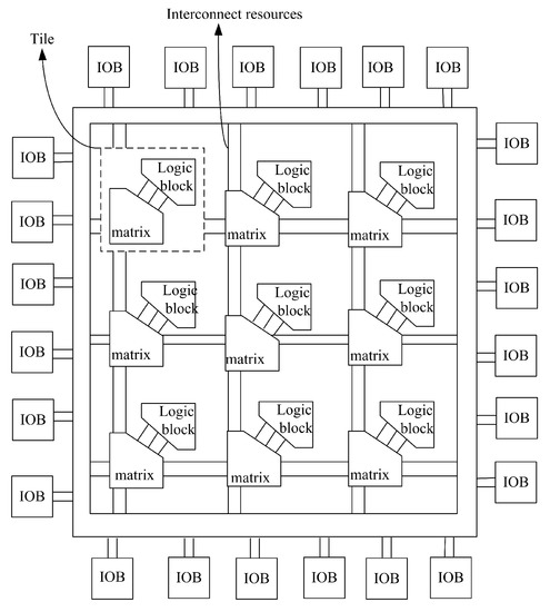
Figure 1.
Typical island-style field programmable gate array (FPGA) architecture.
Routing resources can be divided into lines and PIPs. A large number of PIPs form a matrix, in which the lines are connected to each other through the PIPs. According to the propagating distance, lines are classified into single lines (see Figure 2), double lines (see Figure 3), and hex lines (see Figure 4). The single lines route the matrix signals to the adjacent matrices. The double lines route the matrix signals along four directions to each two contiguous matrices, and the hex lines route the matrix signals along four directions to each six contiguous matrices.
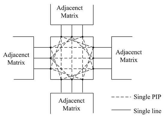
Figure 2.
Single lines and single programmable interconnect points (PIPs).
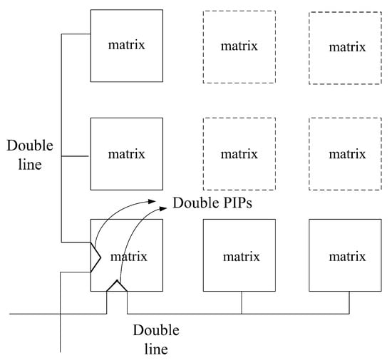
Figure 3.
Double lines and double PIPs.
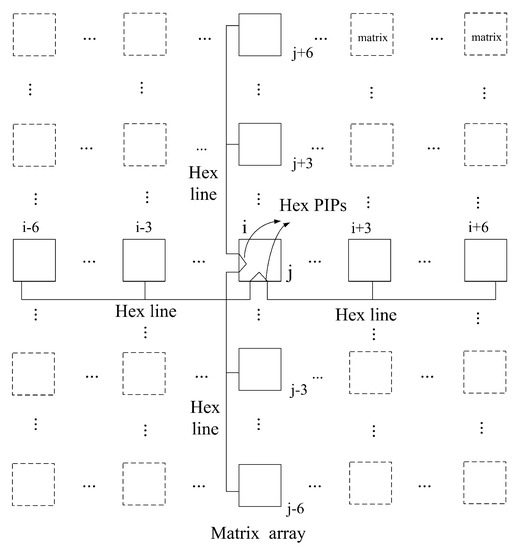
Figure 4.
Hex lines and hex PIPs.
The hex lines can be classified into four categories: eastward lines, westward lines, northward lines, and southward lines. Figure 5 shows a simplified switch matrix in which the lines are named by a combination of numbers and letters. The initial letter indicates the direction (e.g., E means eastward), the adjacent number indicates the type of the line (e.g., 6 means the hex line), the following parameter indicates the direction of data (e.g., MID or END indicates data importing, and BEG indicates data exporting), and the last number indicates the relative position among the hex lines in the same matrix.
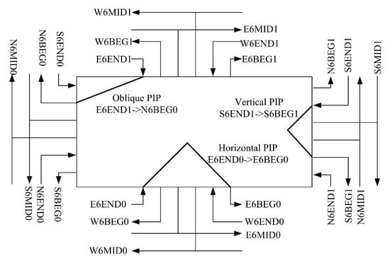
Figure 5.
Hex PIPs in detail (vertical, horizontal, and oblique).
The hex lines can connect to each other via the hex PIPs and can enter the switch matrix of other tiles via the middle point (i.e., at the line with the MID mark) or the ending point (i.e., at the line with the END mark). There are six tiles between the starting point (i.e., at the line with the BEG mark) and the ending point, and three tiles between the starting point and the middle point. The relative position of the hex lines will not be changed during the propagation in the same direction. Take “Horizontal PIP: E6END0 → E6BEG0” and “Vertical PIP: S6END1 → S6BEG1” as examples, the last numbers do not change. However, for the propagation in the oblique direction, the last number in the name of the connected lines may be different. Take “Oblique PIP: E6END1 → N6BEG0” as an example, these two hex lines have different last numbers.
The four edges of the island-style FPGA contain loop-back PIPs, through which the hex lines propagate to the opposite direction. In addition, the direction of the hex lines can be reversed only after passing through the loop-back PIPs, and the relative positions of the hex lines will not be changed. Furthermore, the loop-back PIPs will not change the number of tiles spanned by the hex lines, as shown in Figure 6.
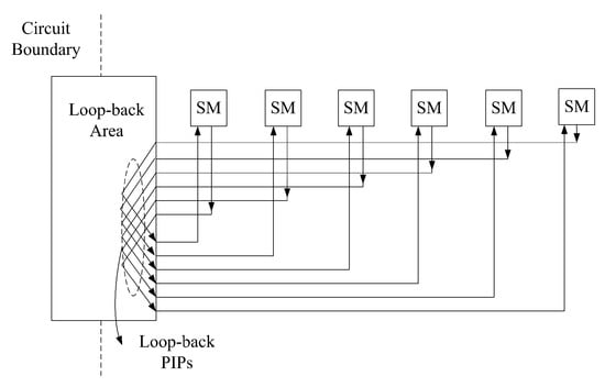
Figure 6.
Loop-back PIPs in detail.
3. HEX PIP Modelling
To summarize the interconnect rules of the hex PIPs, a two-dimension coordinate system based on tiles is set up as shown in Figure 7. For a tile array, the starting point of the coordinate system is in the lower left, and the ending point of the coordinate system is in the upper right. Each tile contains a switch matrix and a function block. According to the type of the logic blocks shown in Figure 1, tiles can be categorized as CLB tile, IOB tile, BRAM tile, DCM tile, and so forth. For the interconnection relationships between the switch matrices and the logic blocks, different types of tiles imply different types of interconnections. However, since the interconnections among the hex lines are fixed, all tiles can be regarded as identical.
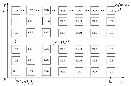
Figure 7.
An FPGA-based two-dimensional coordinate system.
This paper takes the hex lines and their PIPs into account exclusively. Each hex line contains three elements, that is, the coordinates of the starting point, the ending point, and the middle point. It is assumed that the coordinate of the tile where a hex line beginning to propagate is . Then a set of mathematical equations for calculating the coordinates of the middle point and the ending point can be divided into four cases.
Case 1: Propagation towards the left.
For the middle point:
For the ending point:
Case 2: Propagation towards the right.
For the middle point:
For the ending point:
Case 3: Propagation towards the top.
For the middle point:
For the ending point:
Case 4: Propagation towards the down.
For the middle point:
For the ending point:
4. The Proposed Methods for the HEX PIPs Test
4.1. How to Test Vertical & Horizontal PIPs
When the hex lines propagate continuously in the horizontal or vertical direction, a cycle structure will eventually be formed. The corresponding equation for this cyclic structure in the horizontal direction is described as follows:
For in Figure 7, according to Equation (2), if the hex line propagates to the left along the horizontal direction without crossing the loop-back area, the coordinate of the ending point is , where p is the number of repetitions propagated before crossing the left-side loop-back area. After that, the coordinate of the ending point becomes , where q is the number of repetitions propagated after crossing the left-side loop-back area but before crossing the right-side loop-back area. When the loop-back operation occurs twice, it means the hex line will propagate from the right to the left. Then the coordinate of the ending point becomes , and the horizontal distance between this point and is
where, is a positive integer. Obviously, the X-axis coordinate of the nearest point B to is
where % means residual operation.
If , multiple rounds of propagation are needed to make the final ending point back to . Therefore, the number of iterations is defined as
where .
Similarly, in the vertical direction, the Y-axis coordinate of the nearest point C which is closest to is
After N rounds of propagation, an end-to-end cycle structure will be formed, where . The value of N is defined as
A large number of cycles described above can be established to cover all hex lines and hex PIPs in the horizontal and vertical directions. However, such cycle structure cannot be controlled and observed because of having no input and output terminals. Therefore, glue logics used to apply test stimulus and control the transmission of the measured signal need to be inserted as shown in Figure 8. The glue logic which is a buffer in this paper is usually implemented by LUT (look-up table) in the CLB tile. In addition, a PIP should be removed from each cycle. The input and output terminals are provided to the enclosed cycle, and then the unclosed cycle can be further cascaded with other similar structure. After being cascaded through the cycle structure, all hex PIPs in the horizontal and vertical directions are testable.
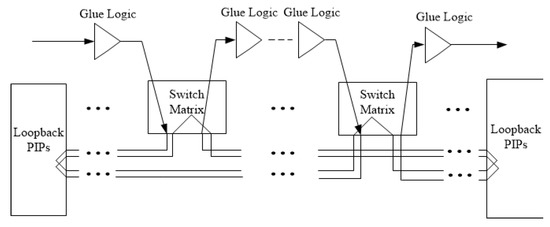
Figure 8.
Horizontal hex line cycle with glue logics.
4.2. How to Test Oblique PIPs
As described in the traditional test structure shown in Figure 9, the PIPs under test, like the single line cascade pattern in Wang et al. [6], constitute an end-to-end cascade structure.
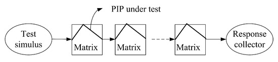
Figure 9.
Traditional cascaded test structure.
Since parts of the hex lines have no PIP in the oblique direction, propagating along the oblique direction will inevitably be connected to a dead end, where the cascade structure can no longer be extended. Hence, it is impossible to construct traditional cascade structure for the hex PIPs in the oblique direction.
Taking into account that the hex PIPs in the oblique direction can hardly be cascaded in the entire circuit, this paper presents a new test structure, through which the hex PIPs can be tested in parallel ways, as shown in Figure 10. Coordinate method is also used to construct such structure. The new test structure contains three parts, that is, stimulus transmission path, PIPs under test, and response transmission path.
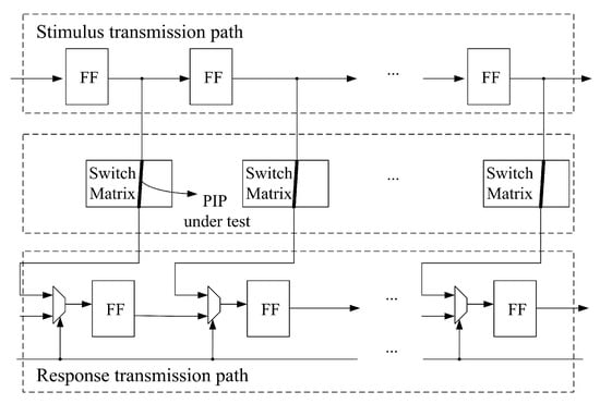
Figure 10.
Test structure of the oblique PIPs.
A flip-flops chain with taps constitutes the stimulus transmission path. Each flip-flop outputs to the next one along the chain to carry the stimuli, whereas the stimuli are sent through the taps in the chain to the corresponding PIPs. Then the PIPs under test obtain global controllability through the flip-flops chain with taps.
Since the test response cannot be output in parallel without sufficient IO resources, this paper refers to the scanning chain test structure in DFT (design for test) to design the response transmission path. A 2:1 multiplexer with a control terminal is inserted at the input of each flip-flop in the chain. By these multiplexers, the response transmission path can alternately implement parallel input and serial output, which makes the tested PIPs globally observable.
The two flip-flop chains shown in Figure 10 can be implemented in CLB tiles. The hex PIPs under test are connected to these two flip-flop chains for rich observability and controllability. The tile position of the flip-flops is calculated by the coordinate method, and the coordinates of the corresponding flip-flops in the stimulus transmission path are obtained by the Equations (1)–(8).
However, it is difficult to cascade the hex PIPs in the oblique direction globally, partial-cascade plan with enclosed cycle is a good choice. Figure 11 divides the island-style FPGA into different regions. All these sections are loop-back areas except section A. The distribution of partial-cascade structure is divided into three cases, that is, in section A, connected with tiles at the boundary, and connected with tiles at the corner.
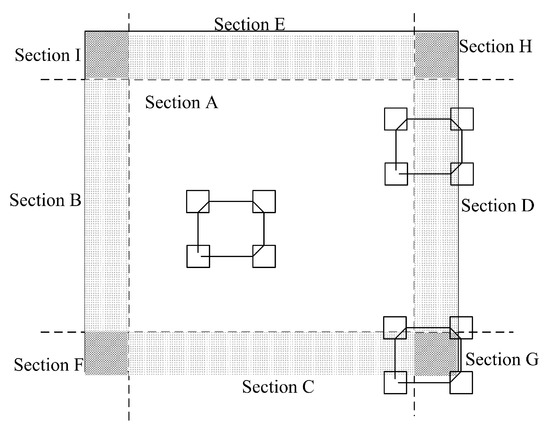
Figure 11.
Digram of loop-back area sections.
If the island-style FPGA is borderless, the partial-cascade structure can migrate to anywhere. However, since the imaginary tiles outside the boundary indicated by the dotted line cannot be tested, as shown in Figure 12, the planned partial-cascade structure cannot be realized anymore in the loop-back areas. It is necessary to reconstruct the partial-cascade structure in the loop-back areas. Take the right boundary (Section D) and the upper right boundary (Section H) as examples, as shown in Figure 13, the corresponding test structures need to be reconstructed to connect to other parts of the partial-cascade structures in section A.
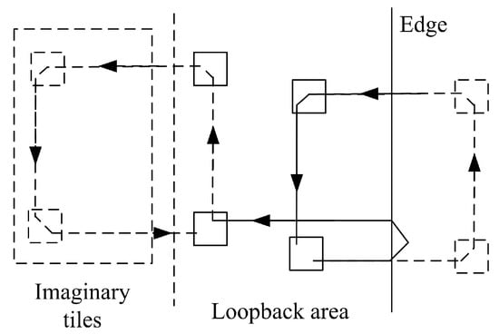
Figure 12.
Partial-cascade structure in the loop-back area.
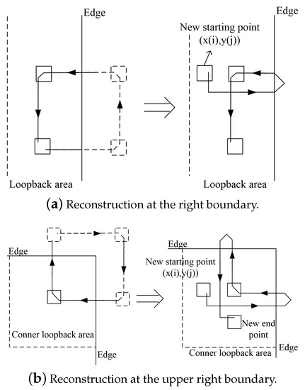
Figure 13.
Reconstruction of the partial-cascade structure in the loop-back area.
Assume that the coordinate of the new starting point is , according to Equation (4), the coordinates of the two adjacent tiles for Section D shown in Figure 13a are and , respectively. Similarly, according to Equation (4) or Equation (6), the coordinate of the upper right tile for Section H shown in Figure 13b is or , depending on the convenience of the designer.
5. Experiments
The proposed method is general for the island-style FPGA with similar hex PIPs structures. For comparison with YAO [17], this paper selects the Virtex4 series XC4VLX60 of Xilinx as the target device. The automatic routing algorithms were designed by the coordinate equations of the hex lines and implemented by C programs. Meanwhile, a fault injection system shown in Figure 14 was developed to validate the proposed algorithms. The fault injection in this paper is mainly to simulate the s-a-open fault, by removing any number of the PIPs in the XDL file to form any number of s-a-open faults.
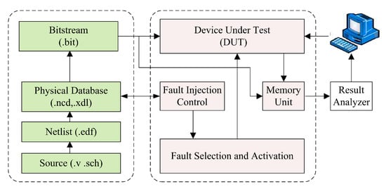
Figure 14.
Block diagram of a fault injection system.
The FPGA implementation is designed by Verilog Editor and ChipScope ILA, and synthesized by ISE tools, based on the principles described in this paper. The fault injection flow from concept to generating the configuration bitstream of the FPGA is also shown in Figure 14. The number of configurations means the number of bitstreams loaded into the corresponding FPGA. Moreover, the total number of hex PIPs and the number of covered PIPs can be calculated by checking the XDLRC file and the XDL file of the ISE tools, respectively. By using the automatic routing algorithms, all proposed test patterns can be implemented and 100% fault coverage of the hex lines and the hex PIPs can be guaranteed.
5.1. Test for the Horizontal & Vertical PIPs
Figure 15 shows the architecture of the XC4VLX60, including various types of tiles arranged in 61 columns and 128 rows, where and . Since and , according to Equations (12) and (14), the number of iterations in the horizontal and vertical directions are all three (, ). In addition, each row of the XC4VLX60 contains 60 mutually independent hex lines, there will be 20 independent end-to-end cycles in one row (). Similarly, each column of the XC4VLX60 contains 60 mutually independent hex lines, there will be 20 independent end-to-end cycles in one column ().
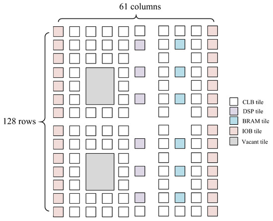
Figure 15.
Architecture of the XC4VLX60.
Table 1 lists the total 70 PIPs in the horizontal and vertical directions in one XC4VLX60 tile. In order to make the proposed end-to-end cycles observable and controllable, glue logics are inserted through the nearest CLB tiles. Figure 16 shows a cycle structure with the glue logic implemented by the adjacent CLB. For a non-CLB tile, for example, BRAM tile, IOB tile, and so forth, the glue logic is provided by the CLB tile located in other rows or columns, as shown in Figure 17. The fault coverage for PIP test can be calculated by
where represents the total number of PIP being tested and represents the number of PIP lost.

Table 1.
PIPs in the horizontal and vertical directions in one XC4VLX60 tile.
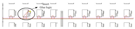
Figure 16.
Insert glue logic for configurable logic block (CLB) tile.
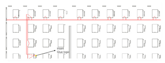
Figure 17.
Insert glue logic for IOB tile.
For PIP test in the horizontal direction, there are 20 end-to-end cycles in one row, each cycle contains one glue logic, so the number of PIP lost is . Meanwhile, the number of the hex PIPs in one direction in a tile of the XC4VLX60 is 35, the total number of hex PIPs in the horizontal and vertical directions in the XC4VLX60 can be obtained by
Therefore, the fault coverage of one time FPGA configuration is
Furthermore, by moving the glue logics to the adjacent tiles and configuring the FPGA again, the fault coverage loss caused by the original glue logics can be compensated, so that the fault coverage can reach 100%.
Similarly, for PIP test in the vertical direction, the number of PIP lost is , and the fault coverage of one time FPGA configuration is
An algorithm for the hex PIPs test in the horizontal direction is shown in Algorithm 1, which is similar to that in the vertical direction. Test patterns are generated through this algorithm in the horizontal and vertical directions respectively, as shown in Figure 18 and Figure 19. With two of such configurations, the fault coverage for hex PIPs test in the horizontal and vertical directions can reach 99.06% and 99.55%, respectively. With four of such configurations, the fault coverage for the hex PIPs test can reach 100%, and the additional two are dedicated for the deleted PIPs due to the glue logic insertion. In addition, since all PIPs in the horizontal and vertical directions shown in Figure 4 can be tested, the fault coverage for the hex lines test can also reach 100% with four of such configurations. Table 2 summarizes the test results of the configuration number and the fault coverage during the fault injection test in the horizontal and vertical directions.
| Algorithm 1 Automatic routing algorithm in the horizontal direction. |
|
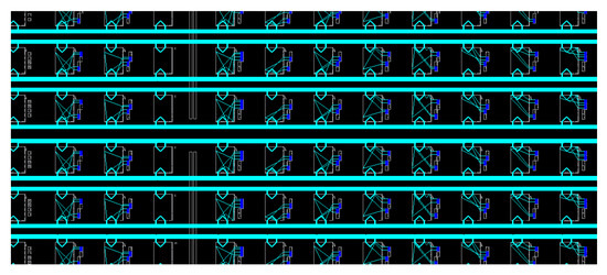
Figure 18.
Test pattern of the hex line & PIPs along the horizontal direction.
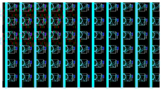
Figure 19.
Test pattern of the hex line & PIPs along the vertical direction.
Table 2.
Summary of the configuration number & fault coverage in the horizontal and vertical directions.
5.2. Test for the Oblique PIPs
Table 3 lists the total 68 PIPs in the oblique direction in one XC4VLX60 tile. Because one tile can only accommodate up to four different routes, one configuration can cover only four oblique PIPs. Therefore, traditional test methods require 17 configurations to complete the test of 68 PIPs in the oblique direction.
Table 3.
PIPs in the oblique direction in one XC4VLX60 tile.
The proposed method designs four kinds of partial-cascade patterns for the oblique PIPs test, as shown in Figure 20, where k represents the hex line number. Based on two of these test patterns, most of the PIPs in Table 3 can be covered, and all PIPs can be divided into four groups, as shown in Table 4.
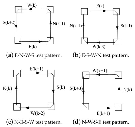
Figure 20.
Four sets of partial-cascade patterns.
Table 4.
Test patterns in the oblique direction in one XC4VLX60 tile.
According to Figure 10, an oblique PIP test point needs two flip-flops and one LUT. However, there are only eight filp-flops and eight LUTs in one XC4VLX60 tile. For the group one in Table 4, the cascade path is “” (See Figure 20a), requiring 14 flip-flops to form seven test rings. Therefore, it needs to be configured at least twice, otherwise the filp-flops will be inadequate. Similarly, for the group two in Table 4, the cascade path is “” (See Figure 20c). It also needs to be configured twice because the corresponding test patterns need 14 flip-flops too. In addition, the group three in Table 4 requires 10 filp-flops to form five test half-rings and needs to be configured twice, and the group four in Table 4 requires four filp-flops and needs to be configured only once. Furthermore, a sufficient number of configurations means sufficient LUT resources, so there is no need to worry about the glue logic insertion.
Since the number of the hex PIPs in the oblique direction in a tile of the XC4VLX60 is 68, the total number of hex PIPs in the oblique direction in the XC4VLX60 can be obtained by
According to Table 4, the cumulative tests of different groups will be carried out in turn, and the corresponding fault coverages are
An algorithm for the hex PIPs test in the oblique direction is shown in Algorithm 2. Moreover, since the middle PIPs which are not considered in this paper have similar structure with the hex PIPs in the oblique direction, this algorithm can also be applied to the middle PIPs test.
| Algorithm 2 Automatic routing algorithm in the oblique direction, which can also be used for the middle PIPs test. |
|
Test patterns are generated through this algorithm in the oblique direction, as shown in Figure 21. Figure 22 shows the details of the PIPs in the oblique direction in a single tile. With six of such configurations, the fault coverage for the hex PIPs test in the oblique direction can reach 97.06%. With seven of such configurations, the fault coverage can reach 100%. Table 5 summarizes the test results of the configuration number and the fault coverage during the fault injection test in the oblique direction.
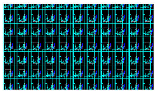
Figure 21.
Test pattern of the hex line & PIPs along the oblique direction.
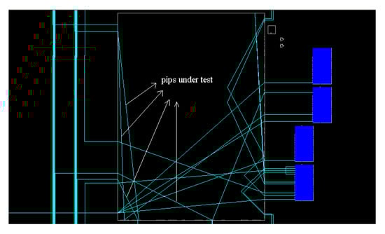
Figure 22.
Details of PIPs under test in the oblique direction.
Table 5.
Summary of the configuration number & fault coverage in the oblique direction.
6. Conclusions
This paper focuses on the hex PIPs in routing resource test of the island-style FPGA and improves the test efficiency of the hex lines. Accordingly, this paper establishes the coordinated model of hex routing resources, and presents the effective cycle test structure in the horizontal and vertical directions and the test structure with partial-cascade patterns in the oblique direction. These test patterns can be generated automatically by the proposed two algorithms.
Table 2 and Table 5 summarize the test results of the configuration number and the fault coverage during the fault injection test. For the XC4VLX60, a total of four configurations are needed to achieve 100% fault coverage for the hex lines, which is much less than that in YAO [17]. To achieve 100% fault coverage for the hex PIPs, a total of 11 configurations are needed. Furthermore, since the double lines and the double PIPs have similar structure with the hex lines and the hex PIPs in the horizontal and vertical directions, whereas the middle PIPs have similar structure with the hex PIPs in the oblique direction, the proposed methods can be applied to the test of these routing resources.
Author Contributions
Conceptualization, F.Z., S.Z., C.G. and L.C.; Formal analysis, F.Z., S.Z., C.G., X.L., H.S., Y.M. and Q.C.; Methodology, F.Z., S.Z. and C.G.; Writing—Original draft, F.Z. and C.G.; Writing—Review & editing, S.Z., L.C., X.L., H.S., Y.M. and Q.C. All authors have read and agreed to the published version of the manuscript.
Funding
This research received no external funding.
Conflicts of Interest
The authors declare no conflict of interest.
References
- Thompson, M. Fpgas Accelerate Time to Market for Industrial Designs. 2004. Available online: http://www.us.design-reuse.com/articles/8190/fpgas-accelerate-time-to-market-for-industrial-designs.html (accessed on 3 November 2020).
- Guo, C.; Zhang, Y.; Chen, L.; Zhou, T.; Li, X.; Wang, M.; Wen, Z. A novel application of FPGA-based partial dynamic reconfiguration system with CBSC. In Proceedings of the 2012 VIII Southern Conference on Programmable Logic, Bento Goncalves, Spain, 20–23 March 2012; pp. 1–4. [Google Scholar] [CrossRef]
- Guo, C.; Zhang, Y.; Wen, Z.; Chen, L.; Li, X.; Liu, Z.; Wang, M. A novel configurable boundary-scan circuit design of SRAM-based FPGA. In Proceedings of the 2011 IEEE International Conference on Computer Science and Automation Engineering, Shanghai, China, 10–12 June 2011; pp. 335–338. [Google Scholar] [CrossRef]
- Yang, Z.; Liang, C.; Wang, J.; Lai, J. A new automatic method for testing interconnect resources in fpgas based on general routing matrix. IEICE Electron. Express 2015, 12, 1–11. [Google Scholar] [CrossRef]
- Renovell, M.; Portal, J.M.; Figueras, J.; Zorian, Y. Testing the interconnect of RAM-based FPGAs. IEEE Des. Test Comput. 1998, 15, 45–50. [Google Scholar] [CrossRef]
- Wang, S.; Huang, C. Testing and diagnosis of interconnect structures in FPGAs. In Proceedings of the Seventh Asian Test Symposium (ATS’98) (Cat. No.98TB100259), Singapore, 2–4 December 1998; pp. 283–287. [Google Scholar] [CrossRef]
- Mishra, B.; Jain, R.; Saraswat, R. Low power BIST based multiplier design and simulation using FPGA. In Proceedings of the 2016 IEEE Students’ Conference on Electrical, Electronics and Computer Science (SCEECS), Bhopal, India, 5–6 March 2016; pp. 1–6. [Google Scholar] [CrossRef]
- Sun, X.; Xu, J.; Chan, B.; Trouborst, P. Novel technique for built-in self-test of FPGA interconnects. In Proceedings of the International Test Conference 2000 (IEEE Cat. No.00CH37159), Atlantic City, NJ, USA, 3–5 October 2000; pp. 795–803. [Google Scholar] [CrossRef]
- Banik, S.; Roy, S.; Sen, B. An integrated framework for application independent testing of fpga interconnect. J. Electron. Test 2019, 35, 729–740. [Google Scholar] [CrossRef]
- Pereira, I.G.; Dias, L.A.; Souza, C.P. A shift-register based bist architecture for fpga global interconnect testing and diagnosis. J. Electron. Test 2015, 31, 207–215. [Google Scholar] [CrossRef]
- Hülle, R.; Fišer, P.; Schmidt, J.; Borecký, J. SAT-ATPG for application-oriented FPGA testing. In Proceedings of the 2016 15th Biennial Baltic Electronics Conference (BEC), Tallinn, Estonia, 3–5 October 2016; pp. 83–86. [Google Scholar] [CrossRef]
- Guo, C.; Chen, L.; Zhang, Y. A novel optimized jtag interface circuit design. Int. J. Electron. Commun. Eng. 2012, 6, 12–16. [Google Scholar]
- Tahoori, M.B. Application-dependent testing of FPGA interconnects. IEEE Trans. Comput. Aided Des. Integr. Circuits Syst. 2005, 24, 409–416. [Google Scholar] [CrossRef]
- Bai, R.; Guo, H.; Wang, Z.; Zhang, Y.; Zhang, F.; Chen, L. FPGA Interconnect Resources Test Based on A Improved Ford-Fulkerson Algorithm. In Proceedings of the 2018 IEEE 4th Information Technology and Mechatronics Engineering Conference (ITOEC), Chongqing, China, 14–16 December 2018; pp. 251–258. [Google Scholar] [CrossRef]
- Zhao, J.; Feng, J.; Lin, T.; Tong, Z. A novel FPGA manufacture-oriented interconnect fault test. In Proceedings of the 2008 9th International Conference on Solid-State and Integrated-Circuit Technology, Beijing, China, 20–23 October 2008; pp. 2091–2094. [Google Scholar] [CrossRef]
- Dixon, B. Built-in Self-Test of the Programmable Interconnect in Field Programmable Gate Arrays. Ph.D. Thesis, Auburn University, Auburn, AL, USA, 2008. [Google Scholar]
- Yao, J. BUILT-in Self-Test of Global Routing Resources in Virtex-4 Fpgas. Ph.D. Thesis, Auburn University, Auburn, AL, USA, 2009. [Google Scholar]
- Banik, S.; Roy, S.; Sen, B. Application-Dependent Testing of FPGA Interconnect Network. IEEE Trans. Very Large Scale Integr. VLSI Syst. 2019, 27, 2296–2304. [Google Scholar] [CrossRef]
- Banik, S.; Roy, S.; Sen, B. Test Configuration Generation for Different FPGA Architectures for Application Independent Testing. In Proceedings of the 2019 32nd International Conference on VLSI Design and 2019 18th International Conference on Embedded Systems (VLSID), Delhi, India, 5–9 January 2019; pp. 395–400. [Google Scholar] [CrossRef]
- Ruan, A.; Huang, H.; Wang, J.; Zhao, Y. A routability-aware algorithm for both global and local interconnect resource test and diagnosis of xilinx sram-fpgas. J. Electron. Test 2016, 32, 749–762. [Google Scholar] [CrossRef]
- Ruan, A.W.; Tian, W.; Ni, B.; Wu, K. A hierarchical switch matrix and interconnect resources test in Virtex-5 FPGA. In Proceedings of the 2014 International Symposium on Integrated Circuits (ISIC), Singapore, 10–12 December 2014; pp. 111–114. [Google Scholar] [CrossRef]


Publisher’s Note: MDPI stays neutral with regard to jurisdictional claims in published maps and institutional affiliations. |
© 2020 by the authors. Licensee MDPI, Basel, Switzerland. This article is an open access article distributed under the terms and conditions of the Creative Commons Attribution (CC BY) license (http://creativecommons.org/licenses/by/4.0/).