Article

Feasibility Study of Interleaving Approach for Quasi-Z-Source Inverter

1
Department of Electrical Power Engineering and Mechatronics, School of Engineering, Tallinn University of Technology, Ehitajate tee 5, 19086 Tallinn, Estonia
2
Educational-Scientific Institute of Electronic and Information Technologies, Chernihiv National University of Technology, 14027 Chernihiv, Ukraine
*
Author to whom correspondence should be addressed.
Electronics 2020, 9(2), 277; https://doi.org/10.3390/electronics9020277
Submission received: 11 December 2019 / Revised: 20 January 2020 / Accepted: 4 February 2020 / Published: 6 February 2020
(This article belongs to the Section Power Electronics)

Abstract

:
This paper presents a comprehensive feasibility study of an interleaving approach for a quasi-Z-source inverter. The state-of-the-art approach revealed that an interleaving approach is often used to improve the efficiency and power density that can overcome the problem of oversized passive elements of quasi-Z-source-based converters. The focus is on the application of the interleaving approach in terms of the comparison of several important parameters of a quasi-Z-source inverter. Our analysis includes losses, capacitor and inductor sizes, as well as semiconductor costs. The theoretical comparison is based on the quasi-Z-source inverter model and the losses model. Simulation and experimental verification of theoretical statements are provided. It was found that a 40% reduction of inductor volume, along with 15–20% of efficiency improvements, are achievable. The results are discussed in the conclusion.

1. Introduction

The Google Little Box Challenge (GLBC) revealed extremely high interest in the topic of high-power density inverters for photovoltaic (PV) applications. It was demonstrated that the extremely high-power density of a power electronics converter is achievable [1,2]. The finalists demonstrated a similar approach using an interleaved full-bridge inverter, wide bandgap (WBG) semiconductors and an active power decoupling circuit [3,4,5]. However, this competition was intended for a converter designed with a narrow input voltage regulation range, whereas string solar inverters commonly have a wide input voltage regulation range. Most of the market solutions have two stages of energy conversion. Advances in WBG materials and their role in power electronics manufacturing have been phenomenal in the last decade. Large-scale manufacturing is also bringing overall costs down, and improving performance handling capability [6].
A Z-source inverter (ZSI) was introduced in 2003 [7] as a single-stage alternative. It was claimed that the converter overcomes the conceptual and theoretical barriers and limitations of the traditional voltage source inverter (VSI) and current source inverter (CSI). ZSIs utilize the shoot-through (ST) cross-conduction states to boost the input dc-voltage by switching on both the top and bottom switches of at least one inverter leg. These inverters can provide maximum power point tracking (MPPT) without any extra dc–dc converter. Their application in various fields is discussed in many papers [8,9,10,11,12,13,14,15,16,17].
At the same time, several papers [18,19,20,21] have disclosed the problems of Z-source networks. In particular, passive component size and overall efficiency are considered a bottleneck in Z-source-based solutions.
Our goal is to study the feasibility of the interleaving approach for a Z-source-based inverter with WBG semiconductors. Our specific aim is to find out if it is reasonable to use approaches applied in the GLBC competition for a Z-source-based inverter.

2. Description of a Case Study System with a Quasi-Z-Source Inverter

The solution in Figure 1 consists of an interleaved 2-level quasi-Z-source inverter (qZSI). Each part includes the quasi-Z-source (qZS) network represented by L1, D1, C1, L2 and C2 for the first branch and L3, D2, C3, L4 and C4 for the second branch. It also has full-SiC 2-level full-bridge inverters represented by switches S1S8; the output filter LF1LF4; CF; and Lg1 and Lg2 feeding the load or connected to the grid.
The 2-level qZSI is described in [22] as a three-phase PV inverter, while the 2-level solution is compared with the 3-level NPC for a single-phase application in [23]. According to the study, a full-SiC 2-level qZSI solution has a clear advantage over the 3-level NPC qZSI solution with Si MOSFETs, in terms of higher efficiency, along with the lower volume of the heatsink, while the volume of passive elements remains the same.
The interleaved 2-level qZSI for a single-phase PV application and the control approaches, including different modulation techniques, are discussed in detail in [23,24,25,26,27]. Our work is devoted to the feasibility study of the interleaving approach in terms of size, efficiency and the overall cost of the converter.
The parameters of the reference system are given in Table 1. The input voltage range is considered from 200 V to 600 V, and the converter was assumed to operate with a rated input current of up to 5 A. In this case, low-frequency (LF) power ripples are mitigated by means of the conventional decoupling capacitor CPV. Many other decoupling techniques are available for this purpose [28,29,30,31,32]. The active power decoupling circuits are relevant for consideration in terms of power density improvements, but are still not effective in terms of the cost. A decoupling capacitor of up to 10 mF can provide the input current ripple of about 10–15% for string solar inverters, which in turn results in the PV panel’s voltage ripple being no higher than 3–4% [33]. These numbers are sufficient to yield an MPPT efficiency of 99%, which is the industrial standard.

3. Component Selection and Comparison

In order to provide correct comparison, the passive and active components were selected according to the predefined parameters. The passive element values of the qZS network for both cases were calculated to provide the desired current and voltage ripple. Usually, the design procedure takes into account the high-frequency (HF) and LF ripple analysis [12]. In this case, the LF ripple is assumed to be eliminated by the input decoupling capacitor CPV. At the same time, the value of the decoupling capacitor is considered to be the same for a single and an interleaved qZSI, and it has no direct impact on the interleaving study. In conclusion, it is required to select the passive components for proper HF ripple mitigation. In the case of a single qZSI, the inductors were selected for the continuous current mode in the basic operating points, which is taken into account in the following equation
L 1 = L 2   >   =   2 * V 2 OUT · T S K L · P · V IN ( V C REF V IN ) V C REF · ( 2 · V C REF V IN )
where L1, L2 are the values of the qZS network inductance, VOUT is the output voltage, VIN is the input voltage, TS is the switching period, KL is the assumed HF ripple of the input current, P is the output power and VC_REF is the reference capacitor voltage. A similar approach was applied for capacitor estimation
C 1 = P · T S 2 · K C 1 · V 2 OUT · V 2 C REF V IN · ( 2 · V C REF V IN )
C 2 = P · T S 2 · K C 2 · V 2 OUT · V PL · ( V C REF V IN ) V IN · ( 2 · V C REF V IN )
where C1, C2 are the values of the qZS network capacitors, and KC1, KC2 are an assumed HF ripple of the capacitor voltage. Passive component values must be large enough to provide the demanded output current quality, converter controllability and low input current ripple in PV applications. Table 2 shows the values selected for our simulation and experimental verification.
As can be seen in the interleaved solution, the values of the inductances are the same, but the relative current ripple is increasing. This is explained by an average current decreasing by splitting the current between the two qZS channels. In this case, capacitor values can be selected twice smaller due to the power flow splitting.
The next task is to select proper active components. Splitting power flow between the two channels with the same resistance may reduce conduction losses up to two times. As a result, interleaving is an approach that enables converter design with extremely high efficiency and power density by means of N channel utilization [34,35]. Evidently, however, this leads to an increase in cost.
Our goal is to specify whether it is possible to design a cost-effective solution using the interleaving approach for the qZSI. Table 3 presents the selected active components and their main parameters. The distributed price was selected as a reference.
As can be seen, all the semiconductors have the same blocking voltage. The nominal rated current is different, but the overall cost of active components is the same. In particular, C2M01612D is twice cheaper than C2M0080120D, but has twice larger drain-source resistance. This means that overall conduction losses in the transistors are expected to be the same.
At the same time, attention should be paid to the different dynamic characteristics. Table 2 shows that semiconductors with a smaller current rate have significantly better dynamic characteristics.
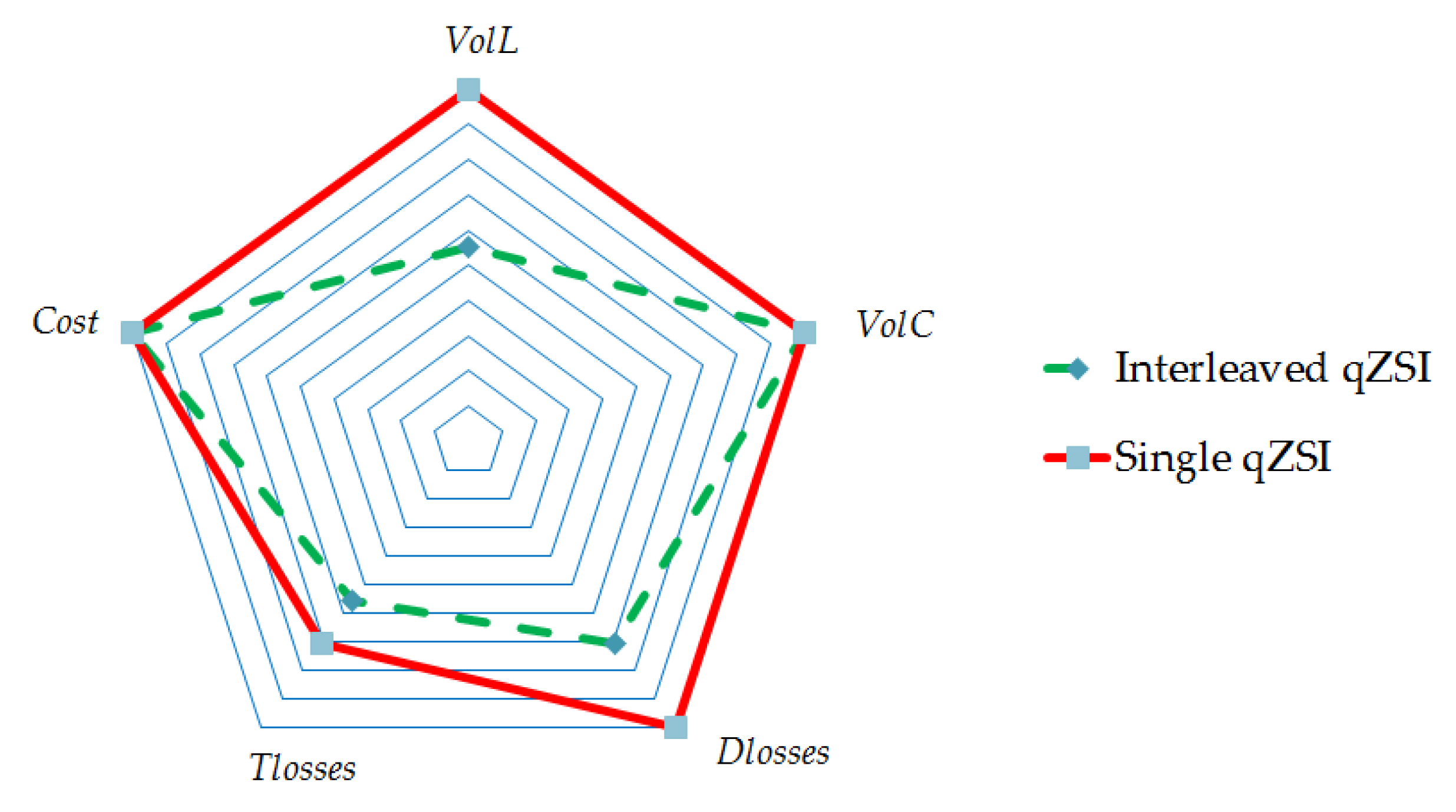
Figure 2 shows a comparative diagram for the estimation of the pros and cons of the interleaving approach for the qZSI. The method of comparison is described in several papers [18,21]; here, we used a modified version. Five parameters were used for comparison: weighted summarized losses of transistors TL, weighted summarized losses of diodes DL, weighted inductors volume VolL, weighted capacitors volume VolC and the weighted cost of semiconductors.
Summarized losses of the single transistor can be estimated by a simplified equation [36,37]
P MOSFET = f · ( t don + t r + t doff + t f 2 I DS V DS + 5 4 Q rr V DS ) + I RMS 2 · R DS
where IDS is a peak current of the transistor averaged over a fundamental cycle, VDS is an averaged peak drain-source voltage at the moment of switching, tdon is a turn-on delay time, tr is a rise time, tdoff is a turn-off time delay, tf is a fall time, RDS is the resistance of the switch open channel, IRMS is the root mean square current value of transistor for one period of the output voltage and Qrr is a reverse recovery charge.
In a similar way, the summarized losses of the single diode can be estimated as in [38]
P DIODE = I F · V F + f · V DR · ( Q r + t R · I )
where VF is the forward voltage drop of the diode, IF is the average current of the diode, VDR is the diode reverse voltage, tR is the diode reverse recovery time and Qr is the reverse recovery charge.
The weighted values of losses are recalculated in the p.u. system, where the largest value of all values is taken as a unit. All the other values are converted through this reference unit. It relates to all other parameters shown in Figure 2.
It is assumed that the volume of the magnetic elements is proportional to the maximum energy that can be accumulated. The same is true for the capacitors.
The total maximum energy that can be accumulated in the inductors is calculated as
E L = i = 1 N L L i · I MAXi 2 2
where Li is the inductance value and IMAXi is the maximum current value through the inductor.
The total maximum energy that can be accumulated in the capacitors is calculated as
E CW = i = 1 N C C i · V MAXi 2 2
where Ci is the capacitance value and VMAXi is the maximum voltage value across the capacitor.
The weighted values of volumes are also recalculated in the p.u. system. It can be seen that the use of the interleaving approach leads to the reduction of the inductor volume. According to Equation (1), the inductance value of the single and the interleaved qZSI remains the same. On the one hand, in the interleaved approach, the power flow through each qZS network is decreased twice, while on the other hand it is assumed that the HF ripple of each inductor in the interleaving approach can be up to two times higher. Phase shifting between the currents of each channel compensates for the ripple increasing. Despite the inductance value of each single inductor being the same for both solutions, according to Equation (6), the maximum energy of the interleaved inductors can be significantly smaller, due to the split current between the two channels.
Furthermore, Figure 2 shows that the interleaving approach may not only provide smaller magnetic elements, but also better efficiency due to the improved dynamic parameters of the semiconductors. It shows that the reduction of losses in active components is expected to be about 30%. These data correspond to the 200 V input voltage and the total input power of 1800 W.

4. Simulation and Experimental Study

In order to verify the theoretical statements, we conducted a simulation and an experimental study. The parameters of the selected topologies are shown in Table 2 and Table 3. The main goal of the simulation study was to verify the calculation of the passive elements and to demonstrate the interleaving approach for ripple cancellation. In all cases, the switching frequency was about 60 kHz.
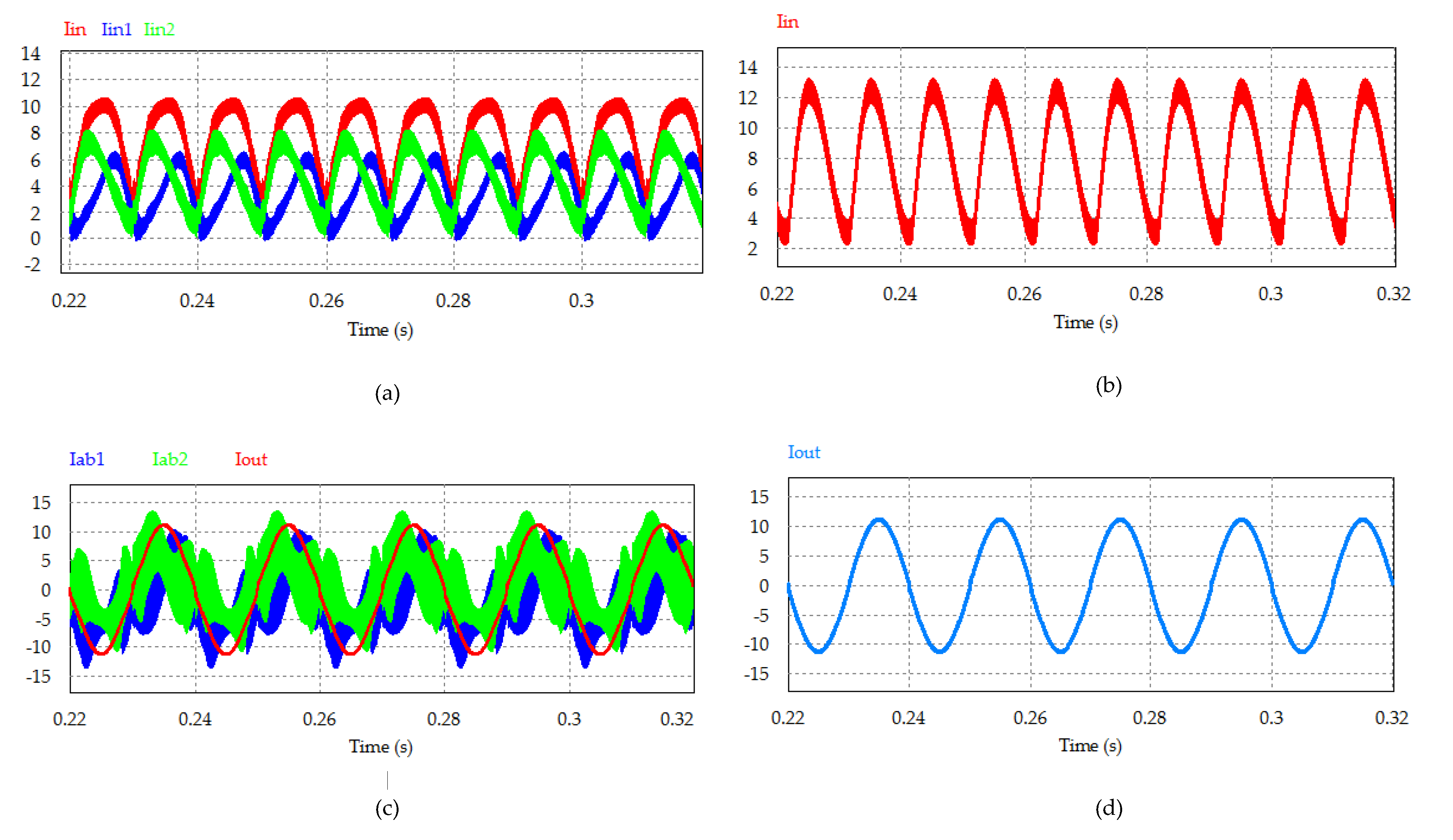
PSIM software was used as a simulation tool. Figure 3 shows our simulation results with the ST implementation at the 200 V input voltage and 1800 W total power. The input current of each channel, along with the summarized input current in the interleaved qZSI solution, are shown in Figure 3a. On the right side (Figure 3b), the input current of a single qZSI is shown. The figure shows that in the interleaved solution, the input current is slightly smaller than in the single solution. Figure 3c,d show output current waveforms, and how the output current is distributed between the two channels. Taking into account the maximum currents through the inductors and corresponding maximum energy accumulated in the inductors, we can claim that the interleaved solution enables a size reduction of about 40%.
At the same time, the most important outcomes are found in the experimental study. A detailed experimental study of a single qZSI is presented in [23]. In the experimental study, we focused on the interleaved qZSI and its comparison with the single 2-level qZSI.
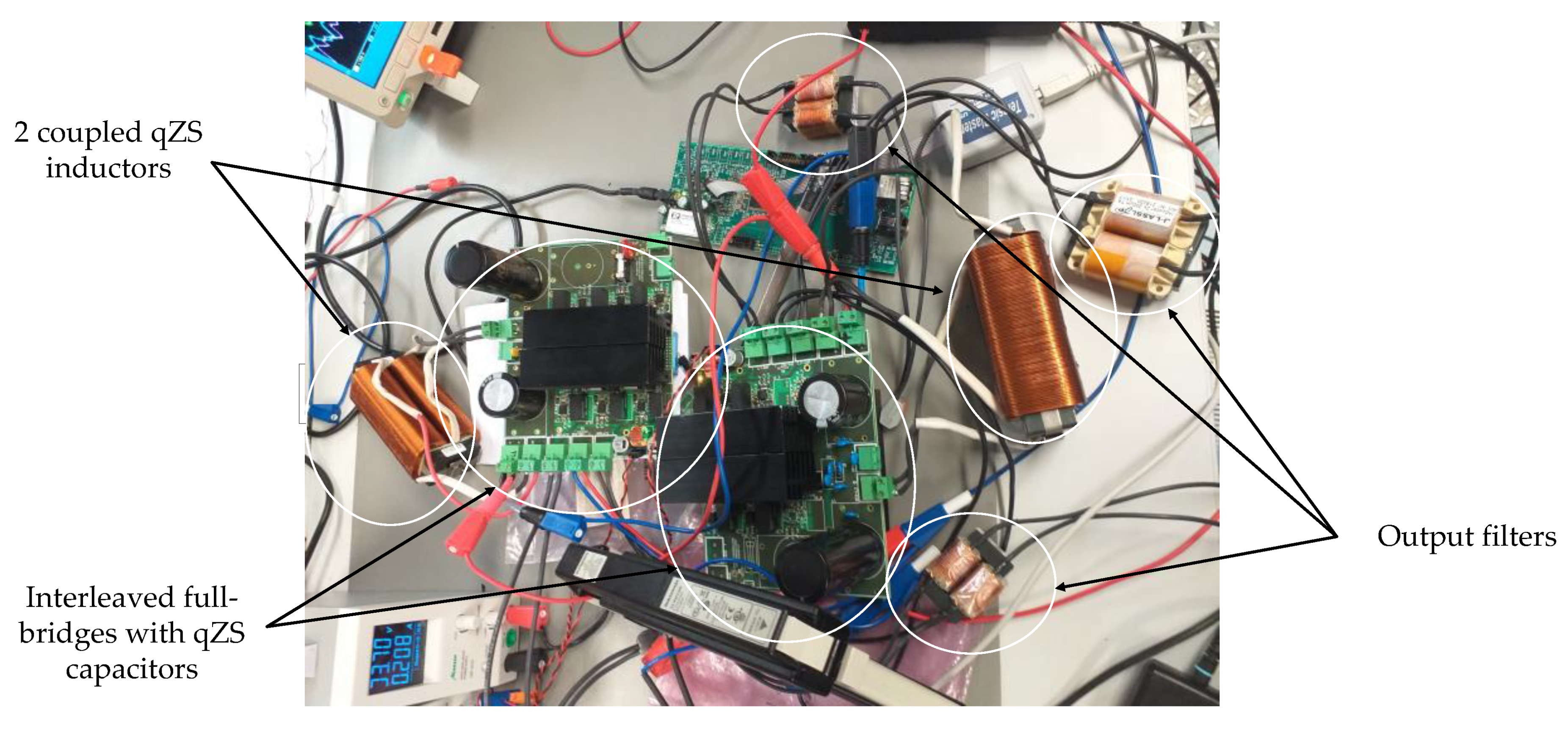
Figure 4 shows the experimental setup of the interleaved qZSI. It comprises two independent channels. The experimental setup also includes measurement equipment, such as the programmable DC power supply (PV array simulator) Chroma 62150H-1000S, a power analyzer YOKOGAVA WT1800 and an oscilloscope Tektronix MSO 4034B.
The dependence of the experimentally measured efficiency on the input voltage with constant input current is illustrated in Figure 5. This shows that the interleaved qZSI has higher efficiency than the single qZSI, which corresponds to the theoretical expectation. At the same time, the improvement of the efficiency is lower than that which was theoretically predicted. This can be explained by non-optimized prototyping and additional losses in the passive components, including wires and connectors.
Experimental data in Figure 6 finalize the verification. The first case (Figure 6a, b) corresponds to the dc source input voltage.
The figures show the input current of each channel, along with the output voltage. A significant double frequency ripple can be seen in both qZSI channels, which is not fully compensated by the interleaving approach. Further double-frequency ripple mitigation is assumed to be achieved by a decoupling capacitor.
On the other hand, in the second case (Figure 6b), the advantage of the interleaving approach is much more obvious, and also has influence on the double frequency ripple. Figure 6c shows the common output current and the distribution between the channels. However, the current distribution between the qZSI channels is not symmetrical, which is explained by the limited tolerance of magnetic components that were essential in the open loop test.
The loss distribution in the interleaved qZSI is shown in Figure 6d. It corresponds to the same operation point with 200 V input voltage and 1 kW input power. As can be seen, significant losses come from the qZS diodes.
Finally, Figure 7a shows the back side of the PCB of the single channel with the heatsink of the qZS diode, while Figure 7b shows the thermal picture that corresponds to the operation point with 200 V input voltage and 1 kW input power.
As can be seen, significant losses come from the qZS diodes whose heatsink is the hottest point (about 70 °C). The analysis of the thermal picture, along with the current measurements, compose the background for the analysis of loss distribution.

5. Conclusions

This work is devoted to the feasibility study of the interleaving approach for the qZSI, taking into account losses, the size of the components and semiconductor costs.
It was demonstrated that the interleaving approach may significantly reduce inductor size and cost by up to 40%. It is also shown that better efficiency can be achieved at the same cost of power semiconductor components. In our case study system, the losses were reduced by 15–20%.
However, these benefits do not guarantee a competitive advantage in mass industrial production. It is necessary to take into account the cost of auxiliary components and the need to control the symmetry of each channel, which will lead to an increase in the number of current sensors. A reliable conclusion can only be obtained in preparation for industrial production, taking into account the cost of all components.

Author Contributions

S.S. conducted the state of the art text writing and design of the experimental setup, O.H. assisted with the development of the idea, experimental tests and paper writing, D.V. provided general supervision and project administration, A.F. assisted with simulation results and O.M. assisted with software development. All authors have read and agreed to the published version of the manuscript.

Funding

This research work was financed in part by the Estonian Centre of Excellence in Zero Energy and Resource Efficient Smart Buildings and Districts, ZEBE, grant 2014-2020.4.01.15- 0016, funded by the European Regional Development Fund, by the Estonian Research Council under Grants PUT1443, and with the support of the European Regional Development Fund and the programme Mobilitas Pluss, under the project MOBJD126, awarded by the Estonian Research Council. It was partially supported by the Ukrainian Ministry of Education and Science (Grant 0117U007260).

Conflicts of Interest

The authors declare no conflict of interest.

References

  1. Bortis, D.; Neumayr, D.; Kolar, J.W. ηρ-Pareto optimization and comparative evaluation of inverter concepts considered for the GOOGLE Little Box Challenge. In Proceedings of the IEEE 17th Workshop on Control and Modeling for Power Electronics (COMPEL), Trondheim, Norway, 27–30 June 2016; pp. 1–5. [Google Scholar]
  2. Morsy, A.; Enjeti, P. Comparison of Active Power Decoupling Methods for High-Power-Density Single-Phase Inverters Using Wide-Bandgap FETs for Google Little Box Challenge. IEEE J. Emerg. Sel. Top. Power Electron. 2016, 4, 790–798. [Google Scholar] [CrossRef]
  3. Kaminski, N.; Hilt, O. SiC and GaN Devices—Competition or Coexistence. In Proceedings of the 2012 7th International Conference on Integrated Power Electronics Systems (CIPS), Nuremberg, Germany, 6–8 March 2012; pp. 1–11. [Google Scholar]
  4. Kroics, K.; Zakis, J.; Suzdalenko, A.; Husev, O. Design Considerations for Gan-Based Microinverter for Energy Storage Integration Into Ac Grid. Latv. J. Phys. Tech. Sci. 2017, 54, 14–25. [Google Scholar] [CrossRef] [Green Version]
  5. Hoene, E.; Ostmann, A.; Marczok, C. Packaging Very Fast Switching Semiconductors. In Proceedings of the 8th International Conference on Integrated Power Electronics Systems, Nuremberg, Germany, 25–27 February 2014; pp. 1–7. [Google Scholar]
  6. Singh, R.; Asif, A.A. Ultra Large Scale Manufacturing Challenges of Silicon Carbide and Gallium Nitride Based Power Devices and Systems. ECS Trans. 2016, 75, 11. [Google Scholar] [CrossRef] [Green Version]
  7. Peng, F.Z. Z-Source Inverter. IEEE Trans. Ind. Appl. 2003, 39, 504–510. [Google Scholar] [CrossRef]
  8. Chub, A.; Vinnikov, D.; Blaabjerg, F.; Peng, F.Z. A Review of Galvanically Isolated Impedance-Source DC–DC Converters. IEEE Trans. Power Electron. 2016, 31, 2808–2828. [Google Scholar] [CrossRef]
  9. Husev, O.; Strzelecki, R.; Blaabjerg, F.; Chopyk, V.; Vinnikov, D. Novel family of single-phase modified impedance-source buck-boost multilevel inverters with reduced switch count. IEEE Trans. Power Electron. 2016, 31, 7580–7591. [Google Scholar] [CrossRef]
  10. Siwakoti, Y.P.; Peng, F.; Blaabjerg, F.; Loh, P.; Town, G.E. Impedance Source Networks for Electric Power Conversion Part-II: Review of Control Method and Modulation Techniques. IEEE Trans. Power Electron. 2015, 30, 1887–1906. [Google Scholar] [CrossRef]
  11. Liu, Y.; Abu-Rub, H.; Ge, B. Z-source/quasi-Z-source inverters: Derived networks, modulations, controls, and emerging applications to photovoltaic conversion. IEEE Ind. Electron. Mag. 2014, 8, 32–44. [Google Scholar] [CrossRef]
  12. Husev, O.; Roncero-Clemente, C.; Romero-Cadaval, E.; Vinnikov, D.; Stepenko, S. Single phase three-level neutral-point-clamped quasi-Z-source inverter. IET Power Electron. 2015, 8, 1–10. [Google Scholar] [CrossRef]
  13. Samadian, A.; Hosseini, S.H.; Sabahi, M.; Maalandish, M. A New Coupled Inductor Non-isolated High step up Quasi Z-Source DC-DC Converter. IEEE Trans. Ind. Electron. 2019. [Google Scholar] [CrossRef]
  14. Nguyen, M.-K.; Tran, T.-T.; Zare, F. An Active Impedance-Source Three-Level T-Type Inverter with Reduced Device Count. IEEE J. Emerg. Sel. Top. Power Electron. 2019. [Google Scholar] [CrossRef]
  15. Vinnikov, D.; Roasto, I. Quasi-Z-Source-Based Isolated DC/DC Converters for Distributed Power Generation. IEEE Trans. Ind. Electron. 2011, 58, 192–201. [Google Scholar] [CrossRef] [Green Version]
  16. Bayhan, S.; Trabelsi, M.; Abu-Rub, H.; Malinowski, M. Finite-Control-Set Model-Predictive Control for a Quasi-Z-Source Four-Leg Inverter under Unbalanced Load Condition. IEEE Trans. Ind. Electron. 2017, 64, 2560–2569. [Google Scholar] [CrossRef]
  17. Komurcugil, H.; Bayhan, S.; Bagheri, F.; Kukrer, O.; Abu-Rub, H. Model-Based Current Control for Single-Phase Grid-Tied Quasi-Z-Source Inverters with Virtual Time Constant. IEEE Trans. Ind. Electron. 2018, 65, 8277–8286. [Google Scholar] [CrossRef]
  18. Husev, O.; Blaabjerg, F.; Roncero-Clemente, C.; Romero-Cadaval, E.; Vinnikov, D.; Siwakoti, Y.P.; Strzelecki, R. Comparison of Impedance-Source Networks for Two and Multilevel Buck-Boost Inverter Applications. IEEE Trans. Power Electron. 2016, 31, 7564–7579. [Google Scholar] [CrossRef]
  19. Burkart, R.; Kolar, J.W.; Griepentrog, G. Comprehensive comparative evaluation of single- and multi-stage three-phase power converters for photovoltaic applications. In Proceedings of the 2012 IEEE International Telecommunications Energy Conference, Scottsdale, AZ, USA, 30 September–4 October 2012; pp. 1–8. [Google Scholar]
  20. Panfilov, D.; Husev, O.; Blaabjerg, F.; Zakis, J.; Khandakji, K. Comparison of three-phase three-level voltage source inverter with intermediate dc-dc boost converter and quasi-Z-source inverter. IET Power Electron. 2016, 9, 1238–1248. [Google Scholar] [CrossRef]
  21. Husev, O.; Shults, T.; Vinnikov, D.; Roncero-Clemente, C.; Romero-Cadaval, E.; Chub, A. Comprehensive Comparative Analysis of Impedance-Source Networks for DC and AC Application. Electronics 2019, 8, 405. [Google Scholar] [CrossRef] [Green Version]
  22. Li, Y.; Anderson, J.; Peng, F.Z.; Liu, D. Quasi-Z-Source Inverter for Photovoltaic Power Generation Systems. In Proceedings of the 2009 Twenty-Fourth Annual IEEE Applied Power Electronics Conference and Exposition, Washington, DC, USA, 15–19 February 2009; pp. 918–924. [Google Scholar] [CrossRef]
  23. Stepenko, S.; Husev, O.; Vinnikov, D.; Roncero-Clemente, C.; Pires Pimentel, S.; Santasheva, E. Experimental Comparison of Two-Level Full-SiC and Three-Level Si–SiC Quasi-Z-Source Inverters for PV Applications. Energies 2019, 12, 2509. [Google Scholar] [CrossRef] [Green Version]
  24. Stepenko, S.; Roncero-Clemente, C.; Husev, O.; Makovenko, E.; Pimentel, S.P.; Vinnikov, D. New interleaved single-phase quasi-Z-source inverter with active power decoupling. In Proceedings of the 2018 IEEE 12th International Conference on Compatibility, Power Electronics and Power Engineering (CPE-POWERENG 2018), Doha, Qatar, 10–12 April 2018; pp. 1–6. [Google Scholar] [CrossRef]
  25. Stepenko, S.; Husev, O.; Pimentel, S.P.; Makovenko, E.; Vinnikov, D. Small Signal Modeling of Interleaved Quasi-Z-Source Inverter with Active Power Decoupling Circuit. In Proceedings of the 2018 IEEE 59th International Scientific Conference on Power and Electrical Engineering of Riga Technical University (RTUCON), Riga, Latvia, 12–13 November 2018; pp. 1–6. [Google Scholar] [CrossRef]
  26. Roncero-Clemente, C.; Husev, O.; Stepenko, S.; Romero-Cadaval, E.; Vinnikov, D. Interleaved single-phase quasi-Z-source inverter with special modulation technique. In Proceedings of the 2017 IEEE First Ukraine Conference on Electrical and Computer Engineering (UKRCON), Kiev, Ukraine, 29 May–2 June 2017; pp. 593–598. [Google Scholar] [CrossRef]
  27. Roncero-Clemente, C.; Stepenko, S.; Husev, O.; Romero-Cadaval, E.; Vinnikov, D. Maximum boost control for interleaved single-phase Quasi-Z-Source inverter. In Proceedings of the IECON 2017-43rd Annual Conference of the IEEE Industrial Electronics Society, Beijing, China, 29 October–1 November 2017; pp. 7698–7703. [Google Scholar] [CrossRef]
  28. Zhang, L.; Ruan, X. Control Schemes for Reducing Second Harmonic Current in Two-Stage Single-Phase Converter: An Overview from DC-Bus Port-Impedance Characteristics. IEEE Trans. Power Electron. 2019, 34, 10341–10358. [Google Scholar] [CrossRef]
  29. Nguyen, M.K.; Tran, T.T.; Lim, Y.C. A Family of PWM Control Strategies for Single-Phase Quasi-Switched-Boost Inverter. IEEE Trans. Power Electron. 2019, 34, 1458–1469. [Google Scholar] [CrossRef]
  30. Zhang, L.; Ruan, X.; Ren, X. Second-harmonic current reduction for two-stage inverter with boost-derived front-end converter: Control schemes and design considerations. IEEE Trans. Power Electron. 2018, 33, 1458–1469. [Google Scholar] [CrossRef]
  31. Zhang, L.; Ruan, X.; Ren, X. One-cycle control for electrolytic capacitor-less second harmonic current compensator. IEEE Trans. Power Electron. 2018, 33, 1724–1739. [Google Scholar] [CrossRef]
  32. Gambhir, A.; Mishra, S.K.; Joshi, A. Power Frequency Harmonic Reduction and its Redistribution for Improved Filter Design in Current-Fed Switched Inverter. IEEE Trans. Ind. Electron. 2019, 66, 4319–4333. [Google Scholar] [CrossRef]
  33. Sullivan, C.R.; Awerbuch, J.; Latham, A.M. Decrease in photovoltaic power output from ripple: Simple general calculation and effect of partial shading. IEEE Trans. Power Electron. 2013, 28, 740–744. [Google Scholar] [CrossRef]
  34. Schrittwieser, L.; Leibl, M.; Haider, M.; Thöny, F.; Kolar, J.W.; Soeiro, T.B. 99.3% Efficient Three-Phase Buck-Type All-SiC SWISS Rectifier for DC Distribution Systems. IEEE Trans. Power Electron. 2019, 34, 126–140. [Google Scholar] [CrossRef]
  35. Kasper, M.; Antivachis, M.; Bortis, D.; Kolar, J.W.; Deboy, G. 4D-Interleaving of Isolated ISOP Multi-Cell Converter Systems for Single Phase AC/DC Conversion. In Proceedings of the PCIM Europe 2016: International Exhibition and Conference for Power Electronics, Intelligent Motion, Renewable Energy and Energy Management, Nuremberg, Germany, 10–12 May 2016; pp. 7698–7703. [Google Scholar] [CrossRef]
  36. Ren, Y.; Xu, M.; Zhou, J.; Lee, F.C. Analytical loss model of power MOSFET. IEEE Trans. Power Electron. 2006, 21, 310–319. [Google Scholar]
  37. Application Note. Available online: http://application-notes.digchip.com/070/70-41484.pdf (accessed on 5 February 2020).
  38. Ma, C.L.; Lauritzen, P.O. A Simple Power Diode Model with Forward and Reverse Recovery. IEEE Trans. Power Electron. 1993, 8, 342–346. [Google Scholar] [CrossRef]
Figure 1. The 2-level interleaved quasi-z-source inverter (qZSI).
Electronics 09 00277 g001
Figure 2. The comparison of the interleaved qZSI versus the single qZSI in terms of weighted values of transistor losses, diode losses, volume of capacitors, volume of inductors and cost of transistors and diodes.
Electronics 09 00277 g002
Figure 3. Simulation results of the interleaved (a,c) and the single qZSI (b,d).
Electronics 09 00277 g003
Figure 4. Experimental setup of the interleaved qZSI.
Electronics 09 00277 g004
Figure 5. Efficiency evaluation of the single qZSI and the interleaved qZSI under different input voltage and constant input current.
Electronics 09 00277 g005
Figure 6. Experimental results of the interleaved qZSI: with an ideal dc source (200 V input voltage) (a,b), and with a photovoltaic (PV) panel as an input source (c), losses distribution in the operation point 200 V, 1 kW (d).
Electronics 09 00277 g006
Figure 7. Printed circuit board (PCB) of one single channel with the heatsink of the qZS diode (a) and its thermal picture in the operation point 200 V, 1 kW (b).
Electronics 09 00277 g007
Table 1. System parameters.
System ParametersValues
Nominal power Pnom, W1800
Nominal input voltage Vnom, V200–600
Nominal input current Inom, A5
Output RMS voltage Vload, V230
Output current THD, %<3
Input current ripple ΔI, %<10
Table 2. Passive elements selection.
Interleaved qZSISingle qZSI
HF current ripple, %7035
qZS inductance L1, L2, mH0.90.9
Maximum current across inductance, A3.45.9
Voltage ripple across C1, %<1<1
qZS capacitor C1, mF0.681.36
Maximum voltage across capacitor C1, V500
Voltage ripple across C2, %<1<1
qZS capacitor C2, mF1.53
Maximum voltage across capacitor C2, V250
Switching frequency, kHz60
Table 3. Active elements selection.
Interleaved qZSISingle qZSI
Transistors
TypeC2M0160120DC2M0080120D
Blocking voltage, V1200
Total Gate Charge, nC3462
Diode reverse recovery charge, nC192105
Turn-on delay time, ns911
Rise time, ns1120
Turn-off time delay, ns1623
Fall time, ns1019
Rds, mOhms16080
Cost, Euro7.515
Diodes
TypeC4D05120AC4D10120A
Blocking voltage, V1200
Forward voltage drop, V1.92.2
Reverse recovery charge, nC23 45
Diode reverse recovery time--
Current, A510
Cost, Euro5.0410.13