Article

Bidirectional Short-Circuit Current Blocker for DC Microgrid Based on Solid-State Circuit Breaker

1
Hubei Provincial Key Laboratory of Efficient Solar Energy Utilization and Energy Storage Operation Control, Hubei University of Technology, Wuhan 430068, China
2
The School of Electrical Engineering, Zhejiang University, Hangzhou 310027, China
*
Author to whom correspondence should be addressed.
Electronics 2020, 9(2), 306; https://doi.org/10.3390/electronics9020306
Submission received: 13 December 2019 / Revised: 6 February 2020 / Accepted: 8 February 2020 / Published: 10 February 2020
(This article belongs to the Section Power Electronics)

Abstract

:
In order to solve the imminent problem in that the traditional protection strategy cannot meet time requirements, together with the fact that the rotational inertia of a DC microgrid is small and short-circuit fault develops rapidly, a bidirectional short-circuit current blocker (BSCCB) based on solid-state circuit breaker for a DC microgrid is proposed. Firstly, the bidirectional current blocking circuit structure is proposed based on the analysis of key components. Then, a top-level differential protection strategy is developed based on the aforementioned proposal. Finally, the performance of the blocking circuit is simulated and verified by experiments. The results show that the proposed method can block short-circuit current within 4 ms, and the response speed of the protection strategy is very fast compared with previous approaches. BSCCB also has reclosing, bidirectional blocking and energy releasing functions. The current blocker proposed in this paper can be reused multiple times and has a promising future in low-voltage DC microgrid application.

1. Introduction

In order to use new energy generation more effectively, microgrid technology, especially DC microgrid technology, has developed rapidly in recent years. Key subcomponents within DC microgrid systems, like distributed power, load and energy storage devices, have drawn great attention in both academia and industry. Such devices play substantial roles in stabilizing the power fluctuation of new energy sources and improving the stability of power supply [1,2]. At the same time, the short-circuit protection problem should be considered and properly handled to address the concern about the reliability of the DC microgrid. However, due to the facts that a DC microgrid has less rotational inertia and that its short-circuit fault develops faster, the protection strategy based on traditional circuit breakers does not fit this circumstance any longer [3,4].
Compared with a traditional mechanical switch, a circuit breaker based on a power electronic switch has shorter operating times and more flexible control modes. It has been proved to be a promising solution for DC microgrid short-circuit protection. According to working principle, circuit breakers based on power electronic switches fall into two categories: solid-state circuit breaker (SSCB) and hybrid circuit breaker, which separates short-circuit current during short circuit with a power electronic switch and reduces power loss with a mechanical switch during normal operation [5,6]. It is also worth noting that, due to its complex structure and difficulties in finding an exact short-circuit current zero-crossing point, the hybrid circuit breaker is not widely used in DC microgrids [7].
A solid-state AC circuit breaker based on charging and discharging structure of a phase-changing capacitor is proposed in [8]. The circuit breaker can switch between normal state and blocking state by controlling the on–off status of a silicon controlled rectifier (SCR). However, the SCR will produce a large overvoltage when it is turned off, which will greatly damage its service life. All solid-state circuit breakers are faced with overvoltage problems caused by shutdown, so overvoltage suppression circuits like resistor–capacitor–diode (RCD) buffer circuit and metal-oxide varistor (MOV) are widely used in solid-state breakers [9,10]. A solid-state circuit breaker specially used in low-voltage DC microgrids is proposed in [11] and [12]. When line-to-line faults occur in the DC bus of the microgrid, the proposed solid-state circuit breaker will eliminate short-circuit faults and use RCD buffer circuit to suppress the overvoltage of the main switch.
Fault current limiter (FCL) based on inductance–capacitance (LC) resonance circuit is an effective traditional current limiting method, and an LC structure-based breaker is proposed in [13]. The structure uses parallel LC resonance to generate large impedance, which limits the rise rate of short-circuit current. It has the advantages of simple structure and high control reliability. Another solid-state fault-current-limiting circuit based on LC series resonant structure is proposed in [14]. During fault mode, the circuit topology is changed into a rectifier bridge to charge the capacitor. When the capacitor voltage is charged to the value larger than input voltage, the fault circuit breaks. A novel solid-state fault current limiter (SSFCL) topology is proposed in [15], which consists of LC series and LC parallel circuits. In normal mode, the impedance of SSFCL is very low due to the influence of series resonance. In current limiting mode, the impedance of SSFCL is very high due to the influence of parallel resonance. A solid-state current limiter based on transformer control was proposed in [16] and [17]. The primary windings of the transformer are connected to the controller and the secondary windings are connected to the main circuit. In case of short-circuit fault, the magnitude of the current on the coupling inductance L in the primary winding is changed to affect the magnitude of the inductive current on the secondary winding, thereby reducing the rise rate of the fault current and keeping the bus voltage at an acceptable level.
High-voltage direct current (HVDC) transmission has always been one of the most important applications of SSCB [18]. At present, the technology is mainly a hybrid high-voltage circuit breaker composed of a mechanical switch and a solid-state switch, which can effectively limit the rise rate of the short-circuit current and suppress the overvoltage generated by the solid-state switch [19,20]. A high-voltage DC circuit breaker combining IGBT with current-limiting inductance was proposed in [21] with large-scale reverse series IGBT circuit structure, whose drawback is that the power loss of IGBT is too large.
On the basis of the advantages and disadvantages of the above methods and in order to meet time requirements in a DC microgrid, a new structure of a bidirectional short-circuit current blocker (BSCCB) based on a solid-state circuit breaker with faster response speed, bidirectional blocking and reclosing functions is proposed. The proposed structure can rapidly eliminate short-circuit current in the main circuit and effectively limit the overvoltage of the main switch. In addition, compared with the traditional breaker circuit, the proposed structure does not require additional power supply to charge the capacitors, which reduces the design cost and size of the circuit.
The structure of this paper is organized as follows: In Section 2, the application background of BSCCB is introduced, and the topology structure and its working mode are analyzed. In Section 3, the control strategy of BSCCB based on differential protection is proposed. In Section 4, the design of main BSCCB components is analyzed. In Section 5, the effectiveness of the proposed method is verified by simulation and experiment, and its dynamic response speed is emphasized.

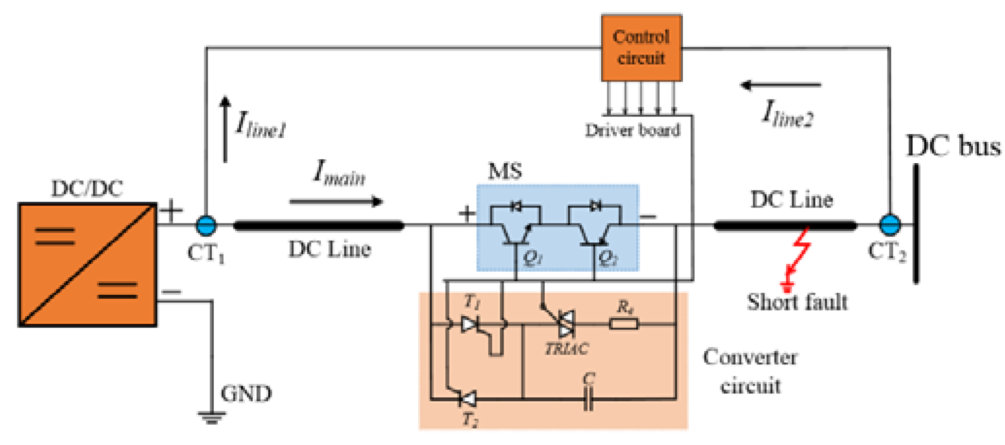
2. Working Principle of the Bidirectional DC Solid-State Circuit Breaker

Figure 1 shows a typical structure of a DC microgrid. The power source, battery and loads are connected together through DC lines.
In order to improve the reliability of the power supply, it is required that when any branch is short circuited in a DC microgrid, it should not affect the normal operation of the DC bus and other branches. Taking the grid-connected branch circuit breaker CB1 as an example, when the DC/AC converter, the transformer or the connecting line has a short-circuit fault, CB1 must cut off the current flowing from DC bus to the grid connection branch in order to avoid DC bus crash. On the contrary, if the DC bus has a short-circuit fault, CB1 must cut off the current flowing from the grid branch to the DC bus. So, the current breaker CB1 should be a bidirectional fast DC breaker. Similarly, the battery also requires a bidirectional DC breaker during the charging and discharging stages. In brief, the bidirectionality of short-circuit faults should be taken into account in all circuits or units involved in energy exchange in a microgrid. Therefore, it is particularly significant to design a circuit breaker with bidirectional short-circuit fault protection capability. It is worth noting that, due to the lower overcurrent capability of DC/AC, DC/DC and other power electronic devices, the circuit breaker must block the fault current in a very fast time. Otherwise, these devices will be out of operation due to overcurrent protection.
Based on the abovementioned requirements for fast and bidirectional circuit breakers, this paper proposes a bidirectional short-circuit current blocker for a DC microgrid based on SSCB, as shown in Figure 2. In Figure 2, the proposed BSCCB is composed of two IGBTs (Q1,Q2) connected in reverse series, two SCRs (T1,T2) connected in reverse parallel, a blocking capacitor C, a bidirectional SCR (TRIAC) and an energy release resistor Re. The current flow path of BSCCB in the whole working cycle is shown in Figure 3. Because blocking capacitor C can be charged bidirectionally, BSCCB can identify and block fault currents in different directions. The current variation curve of BSCCB in one operation cycle is shown in Figure 4. When analyzing the blocking performance of the proposed BSCCB, it is assumed that current flows from DC/DC converter to DC bus, and the analysis of reverse current is the same as the above assumption. A detailed analysis of the working principle of BSCCB in five stages is as follows:

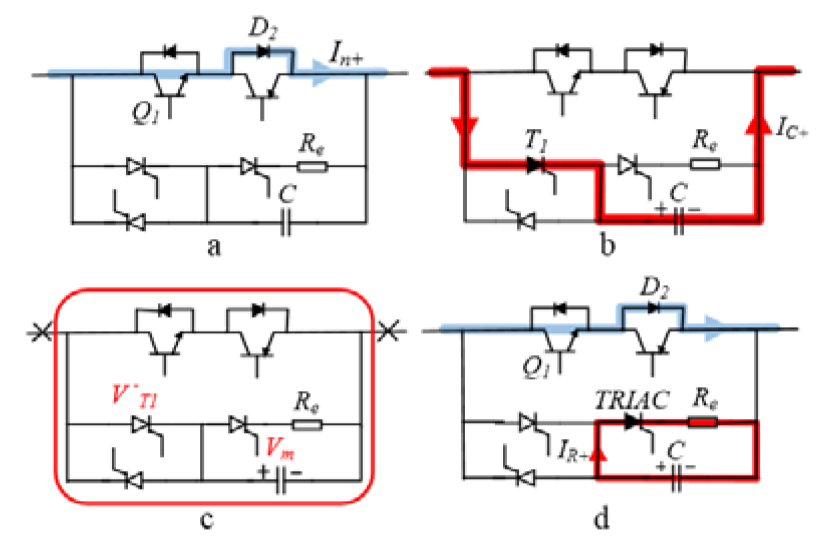
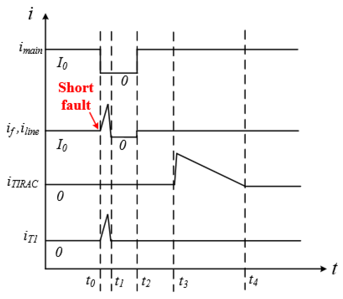
2.1. Normal Operating Mode (t < t0)

In normal operating mode, control signals of Q1 and Q2 are high level, and control signals of T1 and T2 and TRIAC are low level. BSCCB is connected in series with the line, and the rated current In+ flows through IGBT and reverse parallel diodes. Because the conduction voltage drop of IGBT and diode is very low, the BSCCB exhibits a low impedance and does not affect the normal operation of other devices. The line current value is I0, and the current flow path in this mode is shown in Figure 3a.

2.2. Blocking Capacitor Charging Stage (t0 ≤ t < t1)

When BSCCB detects the fault current, it will immediately switch off Q1 and Q2, while switching on T1 at the same time. The fault current is transferred to the blocking branch, and the capacitor C is charged by fault current. Due to the effect of parasitic inductance in the external circuit, fault current if will continue to increase and rapidly reach its peak value, before dropping to zero at t1. This is the blocking capacitor charging stage; the current flow path at this stage is shown in Figure 3b.

2.3. Fault-Current-Blocked Stage (t1 ≤ t < t2)

When fault current is completely absorbed by the capacitor C, the fault line is broken by BSCCB. In the phase of fault current blocking, due to the decrease of fault current, the current through T1 will be reduced to below the maintenance current IH, T1 will be turned off naturally, and capacitor C will not discharge to the external circuit. The circuit operation status of this stage is shown in Figure 3c.

2.4. Reclosing Stage (t2 ≤ t < t3)

The reclosing stage makes the circuit breaker return to normal work mode, and the operation of this stage is just to switch on Q1 and Q2. It is worth mentioning that the energy stored in capacitor C cannot be released until the reclosing operation has finished. Otherwise, due to the clamp of input voltage, the voltage of C cannot be reduced to zero, and the fault current cannot be absorbed effectively when next fault occurs.

2.5. Dump Energy Releasing Stage (t3 ≤ t < t4)

After reclosing stage, by switching on TRIAC, the voltage of capacitor C will be reduced from the stable value Vm to zero. The main switch and energy release loop of BSCCB are working at the same time and do not interact each other. The energy stored in capacitor C is consumed in the form of thermal energy on resistor Re. The use of bidirectional TRIAC makes the control of this stage more convenient and the bidirectional voltage of capacitor C can be released quickly. The current flow direction is shown in Figure 3d.

3. Control Strategy of Proposed BSCCB

3.1. Differential Protection Strategy

The proposed BSCCB is required to have extremely fast response speed in case of short-circuit fault because the DC microgrid has less rotational inertia and the short-circuit fault develops fast. Therefore, this paper adopts current differential protection strategy as the top level protection of BSCCB. The advantage of current differential protection is to compare the current difference between the two ends of the protected line without the influence of voltage criterion and voltage monitoring device; the sensitivity is very high.
The block diagram of the control system is shown in Figure 5. The current sensor monitors the current Iline1 and Iline2 at both ends of the protected line in real time. Iline1 and Iline2 are converted into digital signals through A/D conversion module and digital filter circuit, then obtain the digital signals Im and In by taking absolute values. The differential protection signal Id is obtained by subtracting the Im and In; if the value of Id is higher than the threshold Ker × Is set in the main controller, the driving signal will be generated, which controls the turn-on and turn-off of the switches. It should be noted that the difference between the fault current flowing through both ends of the DC line is large. In order to prevent the controller from generating erroneous instructions during normal operation, an additional protection link is used here. When the Im transmitted to the main controller is less than the reference value Iref set in the main controller, that is, the line current fluctuates within the normal range, the protection is not activated. In addition, the voltage at both ends of the capacitor C will also be transmitted to the main controller as a reference value for triggering TRIAC conduction, if the Vcap reaches a set threshold, TRIAC will be conducting. The boundary condition of differential protection is as follows:
{ I d = | I m I n | I d > K er I s I m > I ref I n > I ref
where Im and In are digital signals converted by A/D; Id is the differential protection current; Ker is the sensitivity coefficient; Iref is the base value of differential protection current to avoid wrong action; Is is the differential threshold current set up according to the rise rate of the fault current of the protected line. It should be noted that the differential protection can be activated only when the three criteria in Equation (1) are satisfied at the same time.

3.2. Switch Timing Sequence Setting

The switching state of each mode is shown in Table 1. At the beginning of short-circuit fault, fault current should be transferred from IGBT branch to SCR branch; the SCR should be closed first before shutting off the IGBT switch. As SCR turns off naturally when the current is zero, the control instruction does not need to control the SCR switching off in the fault-current-blocked stage and energy release stage.

4. Parameter Design

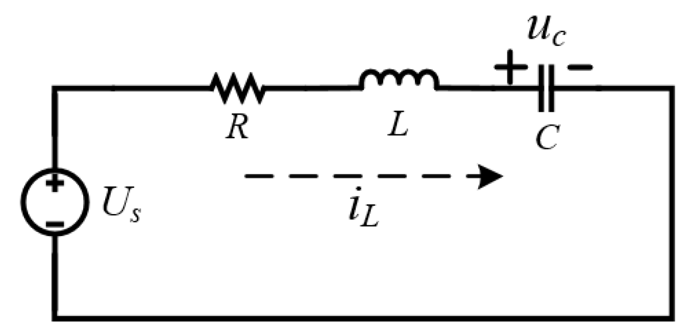
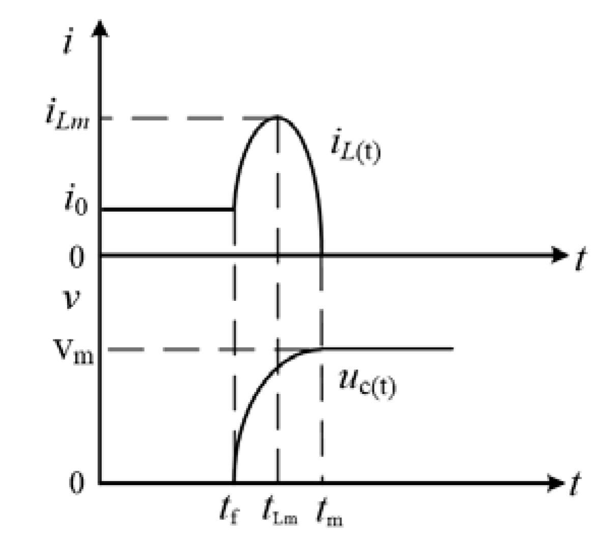
4.1. Capacitor Charging Stage

In the charging stage of capacitor C, the SCR branch starts to work, and the fault current starts to charge capacitor C. The equivalent circuit in this stage is shown in Figure 6.
In Figure 6, R is the equivalent resistance of the line, L is the equivalent inductance of the line in fault mode and U s is the DC voltage. The value of R is relatively small in a real circuit during fault state. Thus, the circuit in Figure 6 is a stateless response, and the corresponding resonance equation can be obtained according to the circuit structure as:
LC d 2 u c dt + RC du c dt + u c = U s
Since there is a constant voltage U s in Equation (2), the expression of capacitance voltage can be written as follows:
u c ( t ) = u c + u c
where u c is the special solution for capacitor voltage and u c is general solution. Given the special solution u c , = U s , the capacitance voltage in Equation (3) is changed to the general solution u c . The variable to the right of the equal sign in Equation (2) is assigned to zero to obtain:
LCs 2 + RCs + 1 = 0
The characteristic root s of Equation (4) is:
{ s 1 = δ + j ω s 2 = δ j ω
where δ = R 2 L is the attenuation coefficient and ω = ω 0 2 δ 2 is the natural oscillation angular frequency; ω 0 = 1 LC is the resonance angular frequency. The above parameters are only related to R, L and C. Generally, the RLC circuit satisfies the following condition in case of short-circuit fault:
R a < 2 L C
The RLC circuit is in an underdamped state, and the capacitor voltage can be expressed as:
u c ( t ) = U s + Ke δ t sin ( ω t + β )
According to the boundary conditions, it can be known that:
{ U s + K sin β = 0 i L ( 0 + ) c = du c ( 0 + ) dt = δ sin β ω cos β = 0
According to Equation (8), the value of parameter K is fixed, allowing the expression of inductance current to be obtained:
i L ( t ) = K ω 0 · L e δ t sin ( ω t )
Because the current flowing through T1 is just one-directional, when the capacitor voltage u c ( t ) reaches the stabilization value Vm, it indicates that the capacitor charging has been completed and the fault current drops to zero instantaneously. The T1 will be switched off naturally, and there is no phenomenon of capacitor reverse discharge. Therefore, when the capacitor voltage reaches Vm or the inductance current drops to zero, the fault lines will be isolated. This means that the capacitor voltage will be maintained at Vm for a long time. Suppose that t m is the time when capacitor voltage has just reached Vm. It can be obtained from Equation (7) as:
t m = π ω
The t m represents the time it takes for capacitor voltage to rise from zero to Vm; it is the blocking time of the fault current. It can be inferred from Equation (10) that the value of t m is only related to ω , which is determined by the parameters R, L and C. Therefore, choosing appropriate capacitance is the key to improve the performance of the circuit breaker. In addition, it can be obtained from Equation (8) as:
i L m = K ω 0 L e β tan β · sin β
where i L m is the peak of the inductance current before the capacitor voltage reaches the stable value Vm, in other words, the maximum value of the fault current is i L m ; it can be seen from Equation (11) that the value of i L m is determined by the R, L, C and U s . The calculation shows that t L m = β ω which is about half the value of the blocking time. The waveforms of capacitor voltage and inductance current are shown in Figure 7.
Under the premise of a certain inductance in the circuit, the relationship between the blocking capacitance C and key variables is shown in Figure 8. Figure 8a shows the relation between the Vm and capacitance C. Since the proposed BSCCB is applied to low-voltage DC microgrid system, three levels of typical low-voltage sources of different ratings were selected for comparative analysis. It can be seen from Figure 8 that under the condition of the same voltage, steady-state voltage is reduced with the increase of capacitance. Figure 8b shows the relation between i L m and capacitance C. It can be seen from the figure that the peak value of i L m increases with the increase of capacitance C at the same voltage. Figure 8c shows the relation between t m and capacitance C. As can be seen from Figure 8c, with the increase of capacitance C, the t m obviously increases. The trajectories of the three curves in Figure 8c are almost identical.
The proposed BSCCB requires shorter blocking time, so the capacity of capacitor C cannot be too large. When selecting the capacity of the capacitor, the blocking time should be given priority. A longer blocking time will bring a larger peak current.

4.2. Energy Release Phase

The equivalent circuit in this stage is shown in Figure 9. In energy release stage, the energy stored in the capacitor C is released in the form of heat energy in the RC circuit through the Re. In this process, the TRIAC plays a role of bidirectional protection, and the circuit structure is first-order RC zero input response. After the switch S is closed:
{ u c = V m e qt i c = V m R e e qt
where u c is the capacitor voltage in the discharge stage and i c is the discharge current of the capacitor; q is the attenuation coefficient, and its value is −1/RC, so its value is only related to the parameters R and C. When the capacitor discharge is completed, the bidirectional switch TRIAC will shut off naturally. After that, there will be no more energy flow in the whole circuit, and the fault current will be cleared. Power loss on resistance Re can be obtained as:
P R e = V m 2 R e e 2 qt
In the process of discharge, the capacitor continuously releases energy and is consumed by Re. Finally, all electrical energy stored in the capacitor is transferred to Re in the form of thermal energy. That is:
E R e = 1 2 CV m 2

4.3. Energy Loss Analysis

The total energy loss of BSCCB consists of conduction loss and switch loss. The conduction loss is mainly caused by the conduction voltage drop of IGBT. Switch losses are mainly produced in SCR branches. The total energy loss can be represented as:
P Tloss P on = V gt · i gt + V ob · i gb
where Vgt and Vob represent the saturation voltage drop of IGBT and SCR, respectively, and their values are constant; i gt and i gb represent the current passing through IGBT and SCR, respectively, and their values change with time.

4.4. Analysis of Parameters

The proposed BSCCB circuit is applied to the microgrid low-voltage DC system, whose voltage level is below 1 kV. From the previous description, it can be seen that the blocking time of BSCCB mainly depends on the capacity of capacitor C, and the discharge time of capacitor C is related to Re. The selection of the important parameters is described in the following subsections.

4.4.1. The Selection of Blocking Capacitor C

The selection of capacitor C is the key to determine the performance of circuit breaker. In order to shorten the blocking time and reduce the peak value of fault current as much as possible, several groups of capacitors with different capacities are selected to analyze and calculate the relevant circuit parameters. In Figure 6, R = 0.1 Ω, L = 5 mH and U s = 600 V. The results are shown in Table 2.
It can be found from Table 2 that: (a) with the increase of capacitance C, the value of Vm gradually decreases; and (b) with the increase of capacitance C, the values of tm and iLm are increased significantly. Considering the design cost, blocking time and overcurrent capability of the circuit, the capacitance of the capacitor chosen for the BSCCB should be as small as possible and the upper limit of the withstand voltage should be low. In addition, choosing a smaller capacity capacitor is conducive to reducing the difficulty of circuit design and the size of the prototype, while being more conducive to improving the flexibility of RC circuit design.

4.4.2. The Selection of Re

Re is also an important parameter affecting the blocking effect of BSCCB. Assuming that the value of capacitance C has been selected, then the value of Vm is also fixed. The relationship between discharge time tr and initial discharge current ic(0+) of the RC energy-release circuit is shown in Table 3. Excessive initial discharge current will lead to a large current rise rate di/dt in the discharge stage, while excessive Re will prolong the discharge time of the capacitor and make the capacitor C discharge incomplete.

5. Performance Evaluation and Analysis

To verify the effectiveness of the proposed BSCCB, simulation and experimental analysis were carried out with the structure shown in Figure 2, whose parameters are shown in Table 4. The simulated fault is a short circuit between DC bus line and ground.

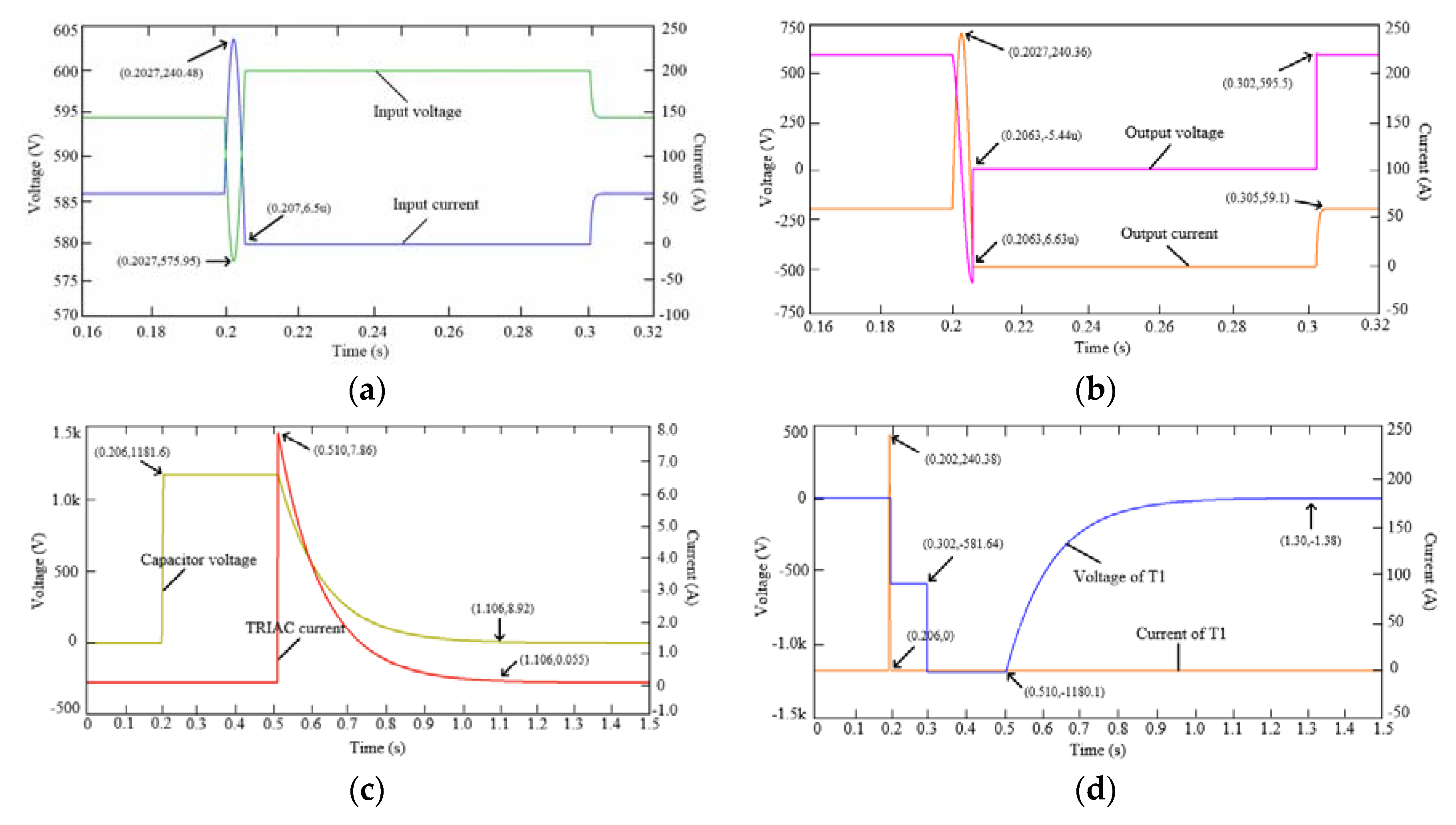
5.1. Simulation Results

The simulated short-circuit fault occurs at 0.2 s. The waveforms of voltage and current at key points are shown in Figure 10.
The waveforms of input voltage and current are shown in Figure 10a. During the time of fault state, the input voltage u in fluctuates very little; it only drops about 20 V and is restored to the rate value within 6 ms, so other power equipment connected in parallel on the bus will not be affected. The input current i in rises to a peak and then drops to zero within 6 ms, which proves that BSCCB successfully isolates the fault line from the protected terminal. When the input voltage drops to the lowest point, the fault current reaches its peak of 240 A. The blocking time is about 6 ms, which is consistent with the results described in the previous section. During the reclosing phase, the input voltage and input current return to the level before the fault, which indicates that the proposed BSCCB can realize the recovery function after the blocking.
The waveforms of output voltage and current are shown in Figure 10b. It can be seen from the Figure 10b that the waveforms of i out and i in are nearly the same. The output voltage u out drops to zero after zero-crossing increases, which is caused by the instantaneous oscillation of inductance Lload and capacitor C. When capacitor C is fully charged, the voltage on inductance Lload will not oscillate and attenuate to zero, which means that the load side and the supply side are successfully isolated.
The voltage waveform of capacitor C and the current waveform of TRIAC are shown in Figure 10c. After the short-circuit fault occurs, the u Cr rises rapidly and reaches 1181 V at 206 ms, which is the value of Vm. The reclosing time of the simulation circuit at 0.3 s, so the storage capacitor C starts to discharge at 0.5 s. It can be seen from Figure 10c that the value of u Cr is 8.9 V at 1.1 s, which is only 0.7% of Vm. It can be considered that the discharge of the capacitor has been completed, so the discharge time is roughly the same as described in Section 4. At the same time, the current i TRIAC has been reduced to zero, and the peak of i TRIAC in the discharge stage is only 7.8 A, which is within the safe range and will not have a significant impact on TRIAC.
In order to ensure BSCCB works efficiently for a long time, the voltage and current waveform on T1 were tested, as shown in Figure 10d. The value of u T 1 in fault-current-blocking stage is 582 V, which is the same as the u out before the fault. This indicates that the load voltage is taken over by T1 after the fault current is blocked. In the reclosing stage, the value of u T 1 is −1180 V, which is equal to the value of −Vm. With the drop of the capacitor voltage, the value of u T 1 gradually decays to zero. The current i T 1 decreases to zero immediately after reaching the peak and does not change any more; this indicates that T1 can be turned off naturally during the blocking stage.
The RC circuit consisting of a 0.8 mF capacitor and a 150 Ω resistor was simulated. Because different RC circuits have different blocking effects, this paper selects six different RC circuits to compare and analyze the proposed bidirectional blockers. The results are shown in Table 5.
In Table 5, I sp represents the peak of the fault current, I r p represents the surge current of the energy release circuit, t b represents the blocking time of the fault current and t e represents the discharge time of the capacitor. As can be seen from Table 5, the only parameter that can affect t b is capacitance C, and the smaller the capacitance, the shorter the blocking time. However, a capacitor with a smaller capacity will produce a larger Vm, which requires capacitors to have better voltage-withstanding performance. In the case of the same Re, smaller capacitance will greatly reduce the discharge time t e of the capacitor, and the change of capacitance has no obvious effect on I rp . Re will affect t e and I rp . When the capacitance is the same, larger Re will prolong the discharge time t e of capacitance but will greatly reduce the value of I rp . Therefore, under the same external conditions, the combination of small capacitance and resistance can shorten the total blocking time (including t b and t e ) and reduce the peak of the fault current accordingly.

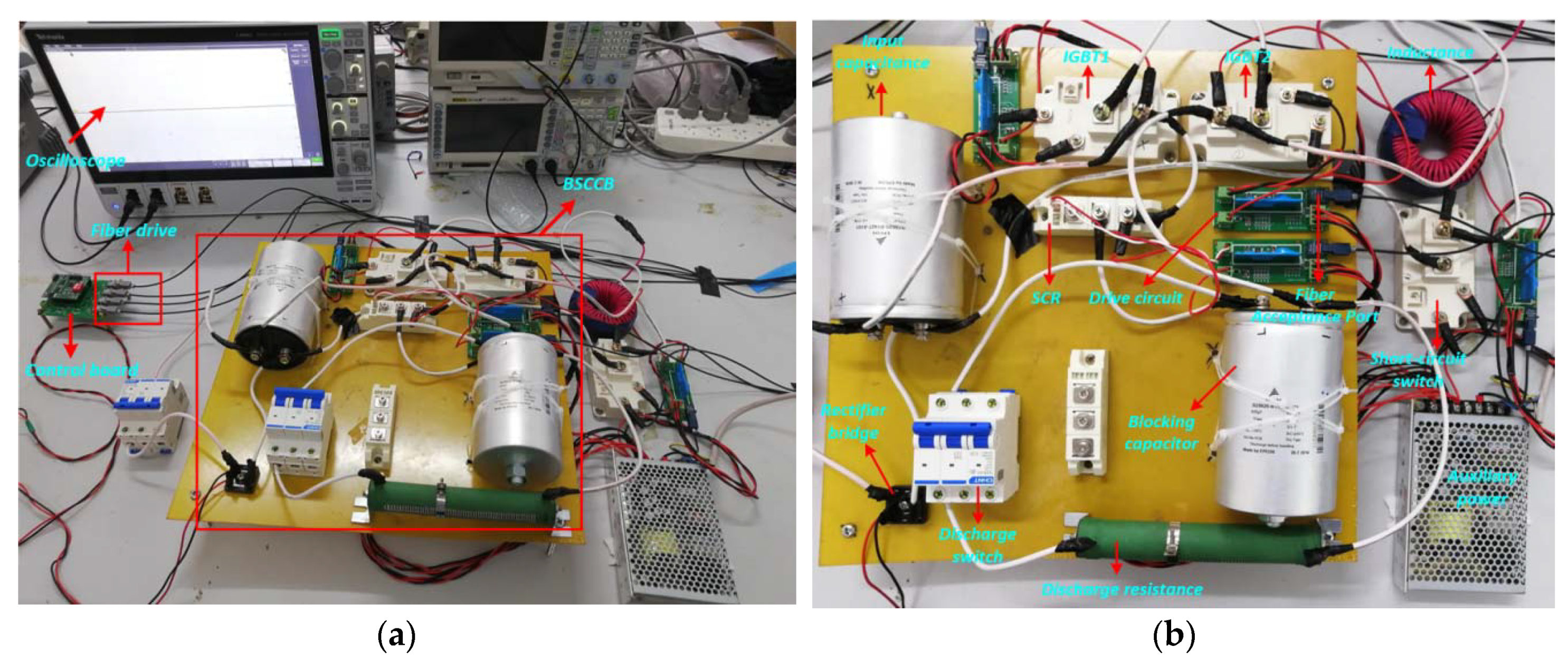
5.2. Experimental Results

In order to further test the performance of the proposed BSCCB, experiments were carried out on the actual circuit. The experimental parameters were consistent with the simulation, and the voltage recovery time of the input side was emphasized. Experimental circuit parameters: C = 0.4 mF, VDC = 220 V and the remaining parameters were the same as in Table 4. The experimental prototype is shown in Figure 11.
The experimental waveforms are shown in Figure 12. As can be seen from Figure 12a, when the short-circuit fault occurs, the fluctuation of DC bus voltage is very small (only about 20 V) and is restored to the rated value within 4 ms. In this way, other electrical equipment connected in parallel on the DC bus will not be affected by this short-circuit fault and will maintain normal operation. The input current rises from the load current to the peak current, then drops to zero. At the same time, the voltage of the blocking capacitor rises to the maximum, and the fault circuit is successfully isolated by BSCCB. It can also be seen from Figure 12b that the peak of the fault current is about 65 A.
In this paper, the mechanical circuit breaker (MCB) and the proposed BSCCB were compared and analyzed, and the breaking performance of MCB was tested. The results are shown in Figure 12c. As can be seen from Figure 12c, the switch-off time of MCB is greater than 10 ms. Compared with the MCB, the proposed BSCCB has faster breaking speed, has no impact on the normal operation of the microgrid system and can reduce the turn-off voltage of the main switch IGBT when breaking the fault current, so it is suitable for the DC microgrid system. However, the differential protection control strategy adopted in this paper does not take into account the communication delay caused during signal transmission, so this is a shortcoming in this design and needs to be further resolved. In addition, the threshold setting of the differential protection signal is also a key part of the circuit design.

6. Conclusions

In this paper, a bidirectional short-circuit current blocking method based on a solid-state circuit breaker for a DC microgrid is proposed. Compared with traditional circuit breakers, the proposed method has faster response speed, bidirectional blocking and reclosing functions. The experimental results show that when the short-circuit fault occurs, the blocking short-circuit current will be blocked within 6 ms. The proposed BSCCB is suitable for a DC microgrid whose rotational inertia is small and whose short-circuit fault develops rapidly. Considering that the proposed BSCCB structure requires faster response speed, the response time of the current sensor and the signal filtering process and the delay of the driving circuit should be improved in future work.

Author Contributions

Conceptualization, L.W. and B.F.; methodology, B.F.; software, L.W.; validation, L.W., B.F. and Y.W.; formal analysis, T.W.; investigation, H.L.; data curation, B.F.; writing—original draft preparation, B.F.; writing—review and editing, Y.W.; project administration, L.W. All authors have read and agreed to the published version of the manuscript.

Funding

This research was funded by the National Natural Science Foundation of China (grant No. 51607060).

Acknowledgments

The author is grateful for the review and guidance of the reviewing experts, and some relevant suggestions from T.W. At the same time, the author would also like to thank the Hubei Provincial Key Laboratory of Efficient Solar Energy Utilization and Energy Storage Operation Control for its support.

Conflicts of Interest

The authors declare no conflict of interest.

References

  1. Rouzbehi, K.; Miranian, A.; Escano, J.M.; Rakhshani, E.; Shariati, N.; Pouresmaeil, E. A Data-Driven Based Voltage Control Strategy for DC-DC Converters: Application to DC Microgrid. Electronics 2019, 8, 493. [Google Scholar] [CrossRef] [Green Version]
  2. Silva, P.; Claudio, M.D.S.M. A Promising Future to DC Power System: A Review. IEEE Lat. Am. Trans. 2017, 15, 1639–1642. [Google Scholar] [CrossRef]
  3. Salomonsson, D.; Soder, L.; Sannino, A. Protection of Low-Voltage DC Microgrids. IEEE Trans. Power Deliv. 2009, 24, 1045–1053. [Google Scholar] [CrossRef]
  4. Virdag, A.; Hager, T.; Doncker, R.W.D. Estimation of short-circuit currents in future LVDC microgrids. Cired Open Access Proc. J. 2017, 2017, 1098–1101. [Google Scholar] [CrossRef] [Green Version]
  5. Abramovitz, A.; Smedley, K.M. Survey of Solid-State Fault Current Limiters. IEEE Trans. Power Electron. 2012, 27, 2770–2782. [Google Scholar] [CrossRef]
  6. Qi, L.; Antoniazzi, A.; Raciti, L. Design of Solid-State Circuit Breaker Based Protection for DC Shipboard Power Systems. IEEE J. Emerg. Sel. Top. Power Electron. 2017, 5, 260–268. [Google Scholar] [CrossRef]
  7. Amir Khan, U.; Lee, J.G.; Amir, F. A Novel Model of HVDC Hybrid-Type Superconducting Circuit Breaker and Its Performance Analysis for Limiting and Breaking DC Fault Currents. IEEE Trans. Appl. Supercond. 2015, 25, 1–9. [Google Scholar] [CrossRef]
  8. Song, S.M.; Kim, J.Y.; Choi, S.S. New Simple-Structured AC Solid-State Circuit Breaker. IEEE Trans. Ind. Electron. 2018, 65, 8455–8463. [Google Scholar] [CrossRef]
  9. Magnusson, J.; Saers, R.; Liljestrand, L.; Engdahl, G. Separation of the energy absorption and overvoltage protection in solid-state breakers by the use of parallel varistors. IEEE Trans. Power Electron. 2014, 29, 2715–2722. [Google Scholar] [CrossRef]
  10. Martin, W.A.; Deng, C.; Fiddiansyah, D. Investigation of low-voltage solid-state DC breaker configurations for DC microgrid applications. IEEE Int. Telecommun. Energy Conf. 2016. [Google Scholar]
  11. Liu, F.; Liu, W.; Zha, X. Solid-State Circuit Breaker Snubber Design for Transient Overvoltage Suppression at Bus Fault Interruption in Low-Voltage DC Microgrid. IEEE Trans. Power Electron. 2017, 32, 3007–3021. [Google Scholar] [CrossRef]
  12. Liu, W.; Yang, H.; Liu, F. An improved RCD snubber for solid-state circuit breaker protection against bus fault in low-voltage DC microgrid. IEEE Future Energy Electron. Conf. 2015.
  13. Meyer, C.; Doncker, R.W.D. LCC analysis of different resonant circuits and solid-state circuit breakers for medium-voltage grids. IEEE Trans. Power Deliv. 2006, 21, 1414–1420. [Google Scholar] [CrossRef]
  14. Radmanesh, H.; Fathi, S.H.; Gharehpetian, G.B. A Novel Solid-State Fault Current-Limiting Circuit Breaker for Medium-Voltage Network Applications. IEEE Trans. Power Deliv. 2016, 31, 236–244. [Google Scholar] [CrossRef]
  15. Ghanbari, T.; Farjah, E. Development of an Efficient Solid-State Fault Current Limiter for Microgrid. IEEE Trans. Power Deliv. 2013, 28, 361–369. [Google Scholar] [CrossRef]
  16. Hagh, M.T.; Abapour, M. DC reactor type transformer inrush current limiter. Iet Elect. Power Appl. 2007, 1, 808–814. [Google Scholar] [CrossRef]
  17. Radmanesh, H.; Fathi, S.H.; Gharehpetian, G.B. Series Transformer-Based Solid-State Fault Current Limiter. IEEE Trans. Smart Grid 2015, 6, 1983–1991. [Google Scholar] [CrossRef]
  18. Hassanpoor, A.; Hafner, J.; Jacobson, B. Technical Assessment of Load Commutation Switch in Hybrid HVDC Breaker. IEEE Trans. Power Electron. 2015, 35, 5393–5400. [Google Scholar] [CrossRef]
  19. Hafner, J.; Jacobson, B. Proactive hybrid HVDC breakers—A key innovation for reliable HVDC grids. In Proceedings of the CIGRE International Symposium on The Electric Power System of the Future, Italy, Bologna, 13–15 September 2011; pp. 1–9. [Google Scholar]
  20. Dujic, D.; Steinke, G.K.; Bellini, M.; Rahimo, M.; Storasta, L.; Steinke, J.K. Characterization of 6.5 kV IGBTs for high-power medium frequency soft-switched applications. IEEE Trans. Power Electron. 2014, 29, 906–919. [Google Scholar] [CrossRef]
  21. Li, S.; Zhao, C.; Xu, J. A new topology for current-limiting solid-state HVDC circuit breaker. In Proceedings of the 2016 IEEE 2nd Annual Southern Power Electronics Conference (SPEC), Auckland, New Zealand, 5–8 December 2016. [Google Scholar]
Figure 1. Structure of typical DC microgrid.
Electronics 09 00306 g001
Figure 2. Typical topology of the bidirectional short-circuit current blocker (BSCCB) in DC microgrid.
Electronics 09 00306 g002
Figure 3. Current flow path of BSCCB: (a) Normal Operating Mode;(b) Blocking Capacitor Charging Stage;(c) Fault-Current-Blocked Stage;(d) Reclosing Stage and Dump Energy Releasing Stage.
Electronics 09 00306 g003
Figure 4. Typical current curves of BSCCB.
Electronics 09 00306 g004
Figure 5. Diagram of differential protection control strategy.
Electronics 09 00306 g005
Figure 6. Equivalent circuit of capacitor charging stage.
Electronics 09 00306 g006
Figure 7. Capacitor voltage and inductance current curves.
Electronics 09 00306 g007
Figure 8. Relationship between capacitance C and key variables: (a) the relationship between Vm and C; (b) the relationship between iLm and C; (c) the relationship between tm and C.
Electronics 09 00306 g008
Figure 9. Energy release phase equivalent circuit diagram.
Electronics 09 00306 g009
Figure 10. The waveforms of voltage and current at key points: (a) waveform of input voltage u in and input current i in ; (b) waveform of output voltage u out and output current i out ; (c) waveform of Cap voltage u Cr and TRIAC current i TRIAC ; (d) waveform of voltage u T 1 and current i T 1 on T1.
Electronics 09 00306 g010
Figure 11. Experimental prototype: (a) experimental platform; (b) BSCCB.
Electronics 09 00306 g011
Figure 12. Experimental waveforms: (a) waveforms of input voltage and output current (time: 4 ms/div; voltage: 75 V/div; current: 30 A/div); (b) waveforms of Cap voltage and output current (time: 4 ms/div; voltage: 150 V/div; current: 30 A/div); (c) output voltage and output current waveforms of mechanical circuit breaker (MCB) at short-circuit instant (time: 4ms/div; voltage: 75 V/div; current: 30 A/div).
Electronics 09 00306 g012
Table 1. Switching state of each mode.
SwitchQ1/Q2T1/T2TRIAC
Mode
Normal modeONOFFOFF
Capacitor chargingOFFONOFF
Circuit blockingOFFOFFOFF
ReclosingONOFFOFF
Energy releaseONOFFON
Table 2. Relationship between Vm, iLm, tm and C.
C (mF)Vm (V)iLm (A)tm (ms)
0.113331042.0
0.212561332.7
0.412121774.0
0.611912105.0
0.811792396.0
1.011712657.0
1.211652887.3
1.411593097.9
1.611513478.5
Table 3. Relationship between ic(0+), tr (s) and Re.
R (Ω)ic(0+) (A)tr (s)
5024.00.2
10011.80.4
1507.80.6
2005.90.8
2504.71.0
Table 4. Simulation parameters.
ParameterValueInstructions
Rs0.1 ΩInput resistance
Ls1 uHInput inductance
Rload10 ΩLoad resistance
Lload5 mHLoad inductance
C0.8 mFBlocking capacitor
Re150 ΩRelease resistance
VDC600 VDC bus voltage
Table 5. Effects of different RC circuits on blocking performance.
ParametersVm I s p I r p t b t e
RC Circuit
0.1 mF, 50 Ω1335 V105 A26.6 A2 ms30 ms
0.1 mF, 150 Ω1335 V105A8.9 A2 ms90 ms
0.8 mF, 50 Ω1181 V240 A23.6 A6 ms380 ms
0.8 mF, 150 Ω1181 V240 A7.8 A6 ms800 ms
1.6 mF, 50 Ω1156 V330 A23 A9 ms1500 ms
1.6 mF, 150 Ω1156 V330 A7.7 A9 ms1600 ms

