A Buck-Boost Transformerless DC–DC Converter Based on IGBT Modules for Fast Charge of Electric Vehicles

 ,
,  and
and 
Abstract
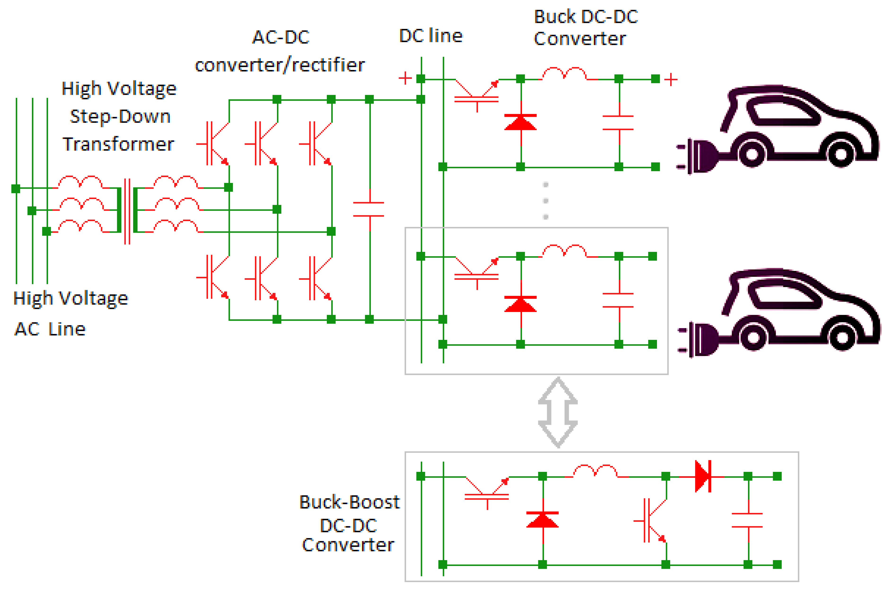
:1. Introduction
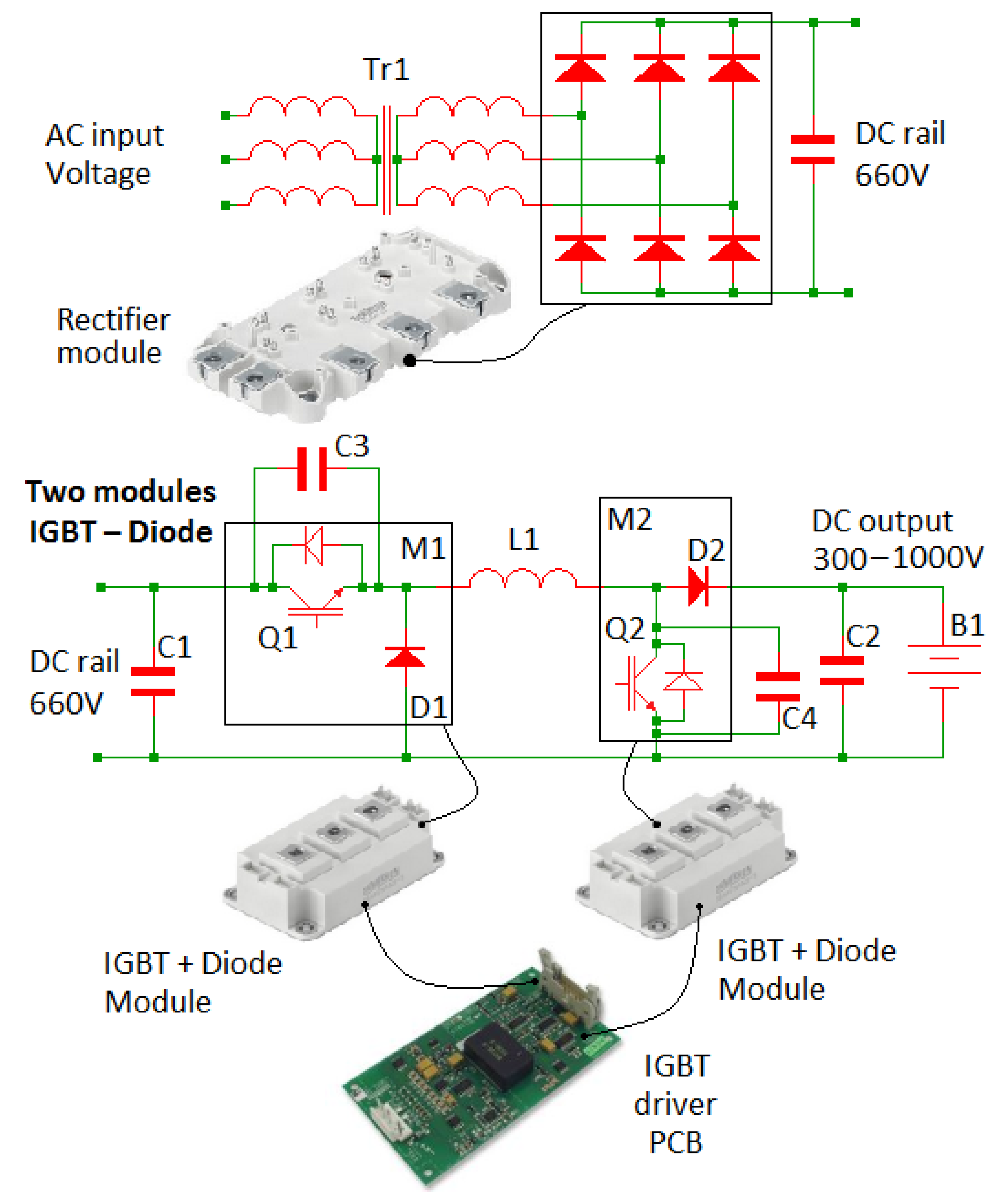
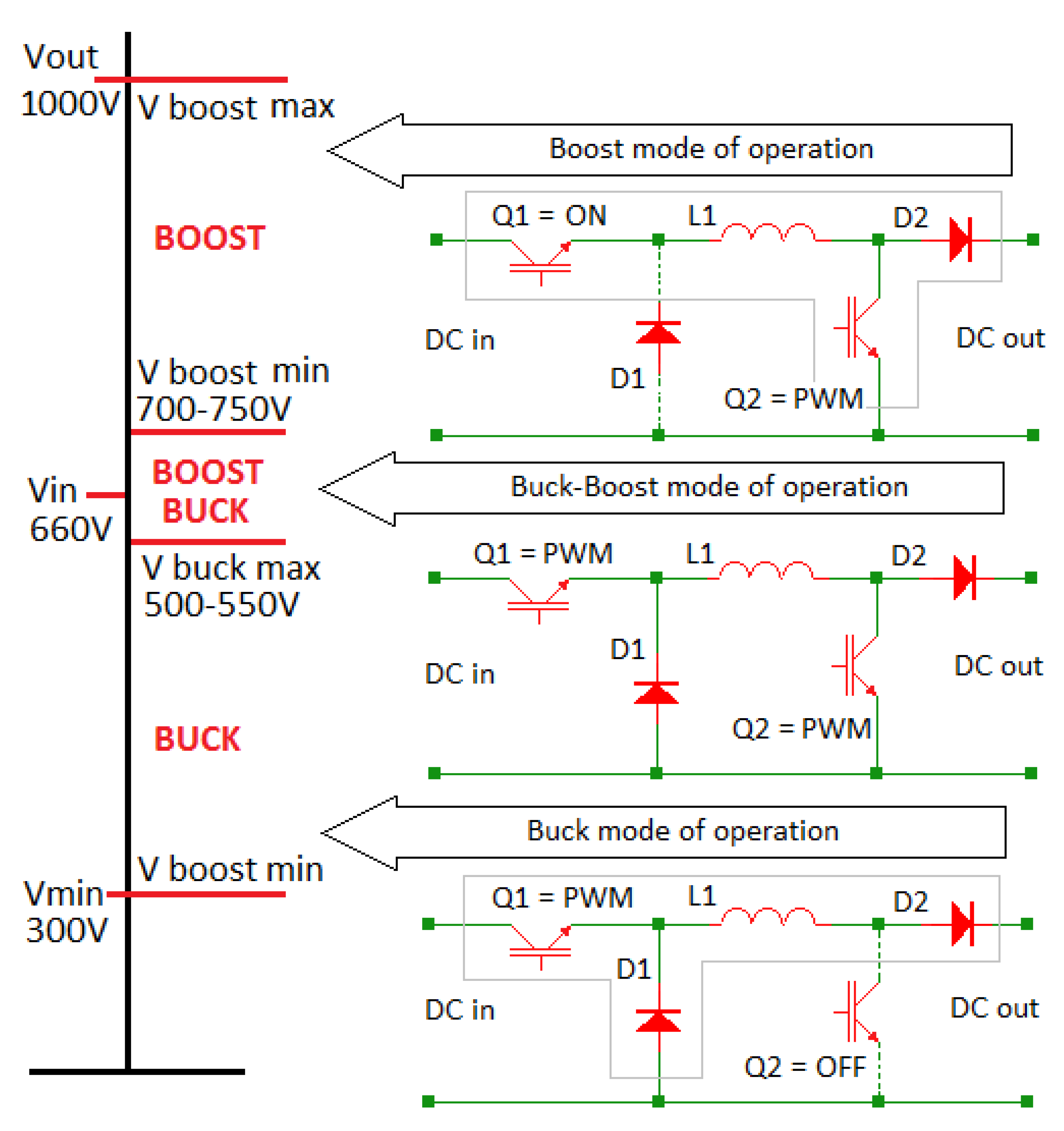
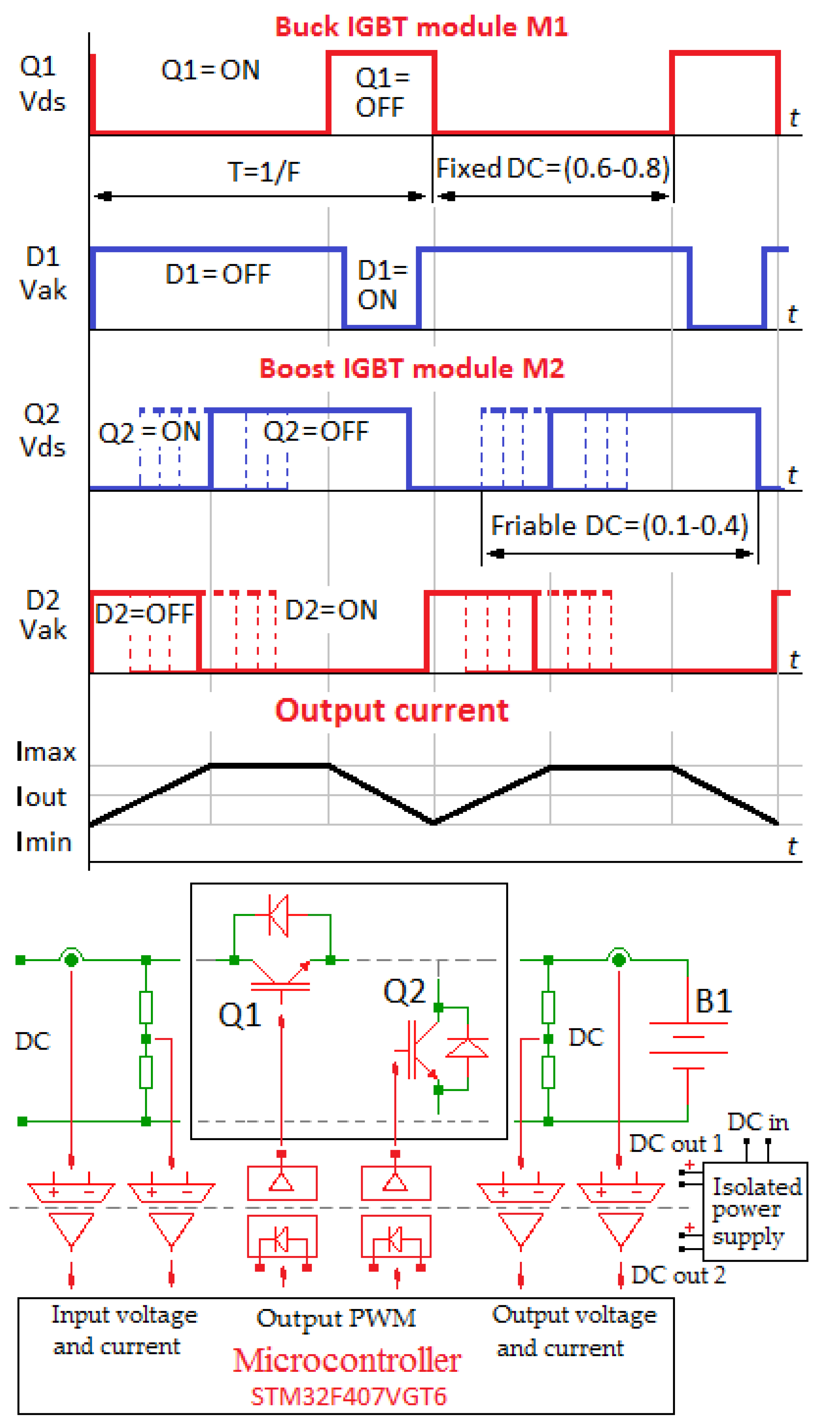
2. Analysis of the Proposed Converter
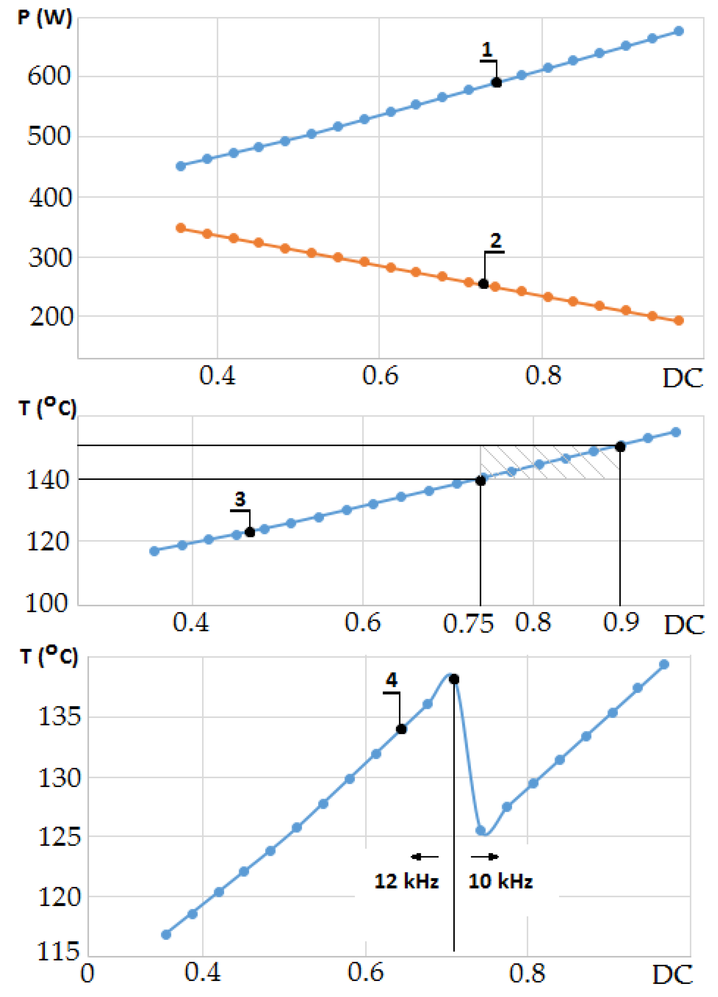
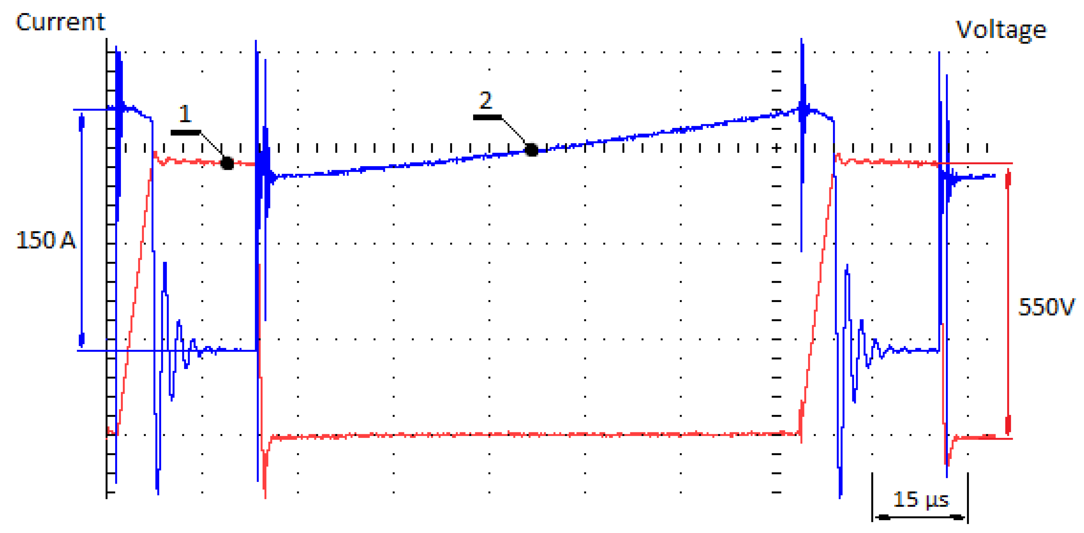
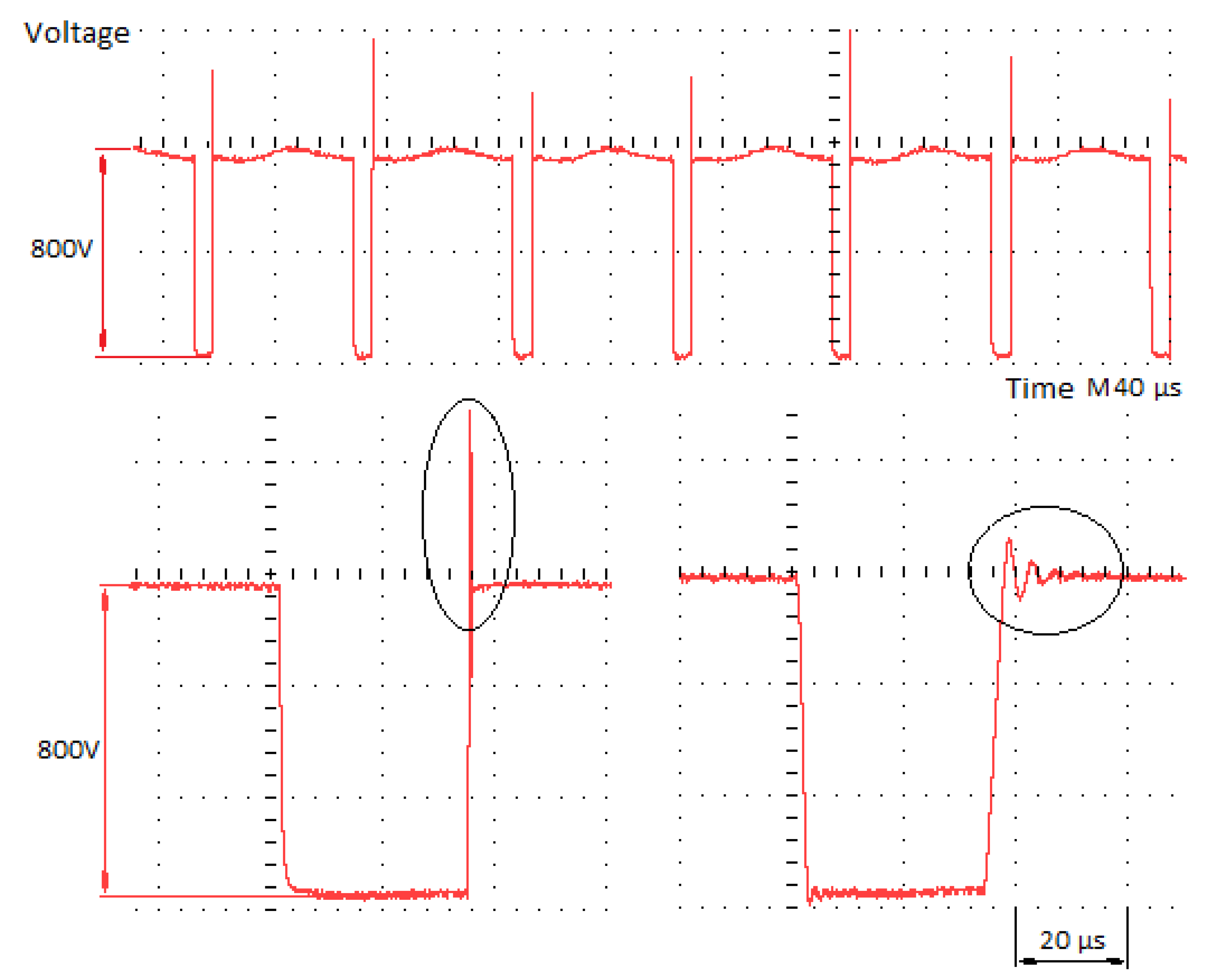
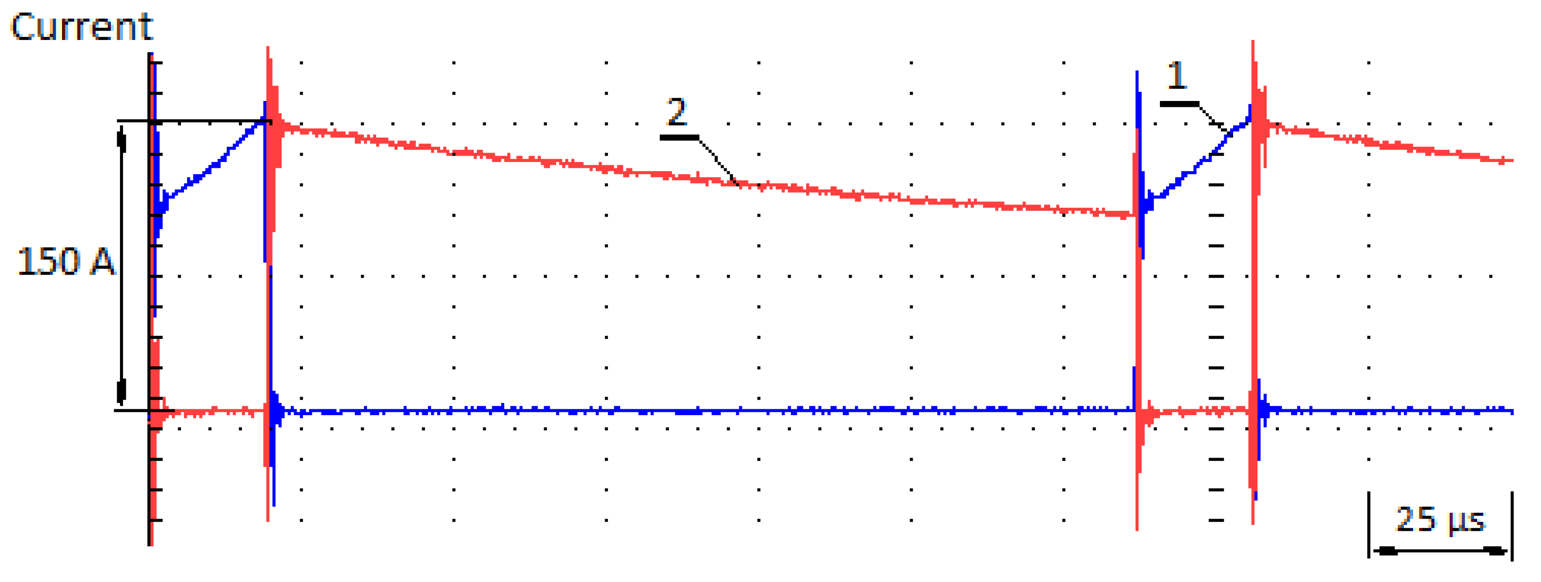
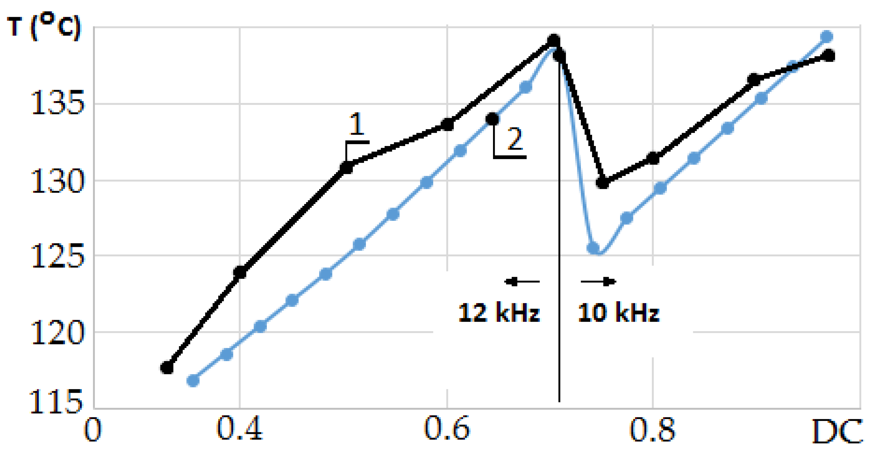
3. Experimental Data
4. Conclusions.
Author Contributions
Funding
Acknowledgments
Conflicts of Interest
Appendix A

| Type | Voltage [V] | Current [A] | Eon [mJ] | Eoff [mJ] | Er [mJ] | Rth(j-c) [K/W] |
|---|---|---|---|---|---|---|
| Semikron [49] | ||||||
| SEMiX452GAL126HDs | 1200 | 319 | 35 | 45 | 33 | 0.15 |
| SKM400GB125D | 300 | 17 | 18 | 16 | 0.05 | |
| SKM400GAL126D SKM400GAR126D | 300 | 29 | 48 | 27 | 0.08 | |
| SEMiX302GAL12E4s SEMiX302GAR12E4s | 356 | 30 | 44 | 19 | 0.096 | |
| SKiiP39GB12E4V1 | 312 | 20 | 49.7 | 30.2 | 0.19 | |
| SEMiX503GB126HDs | 466 | 20 | 44 | 32.5 | 0.08 | |
| Infineon [50] | ||||||
| FF300R12KS4HOSA1 | 1200 | 300 | 25 | 15 | 15 | 0.064 |
| FF300R12KE3HOSA1 | 440 | 25 | 44 | 26 | 0.15 | |
| FF450R12KT4 | 450 | 30 | 40 | 35 | 0.11 | |
| Mitsubishielectric [51] | ||||||
| CM300DX-24T1 | 1200 | 300 | 36 | 29 | 18 | 0.1 |
| CM450DX-24T1 | 450 | 56.6 | 42 | 23 | 0.08 | |
| Fuji electric [52] | ||||||
| 2MBI300U4H-120 | 1200 | 300 | 17 | 19 | 10 | 0.08 |
| 2MBI400VD-120-50 | 400 | 16 | 18 | 17 | 0.045 | |
| 1MBI200VA-120L-50 | 200 | 15 | 22 | 18 | 0.17 | |
| 1MBI900VXA-120PC-50 1MBI900VXA-120PD-50 | 900 | 20 | 40 | 15 | 0.03 | |
| Microsemi [53] | ||||||
| APTGT200A120G | 1200 | 400 | 20 | 20 | 18 | 0.14 |
| IXYS [54] | ||||||
| MIXA225PF1200TSF | 1200 | 360 | 20 | 27 | 11.7 | 0.14 |
| MID 300-12A4 | 330 | 32 | 29 | - | 0.15 | |
| MDI 300-12A4 | ||||||
| MID 550-12 A4 MDI 550-12 A4 | 460 | 64 | 59 | - | 0.05 | |
References
- Wolbertus, R.; Hoed, R.V.D. Electric Vehicle Fast Charging Needs in Cities and along Corridors. World Electr. Veh. J. 2019, 10, 45. [Google Scholar] [CrossRef] [Green Version]
- Khan, W.; Ahmad, F.; Alam, M.S. Fast EV charging station integration with grid ensuring optimal and quality power exchange. Eng. Sci. Technol. Int. J. 2019, 22, 143–152. [Google Scholar] [CrossRef]
- Neaimeha, M.; Salisbury, S.; Hill, G.; Blythe, P.; Scoffield, D.; Francfort, J. Analysing the usage and evidencing the importance of fast chargers for the adoption of battery electric vehicles. Energy Policy 2017, 108, 474–486. [Google Scholar] [CrossRef]
- Gnanna, T.; Funkea, S.; Jakobsson, N.; Plotza, P.; Sprei, F.; Bennehag, A. Fast charging infrastructure for electric vehicles: Today’s situation and future needs. Transp. Res. Part. D Transp. Environ. 2018, 62, 314–329. [Google Scholar] [CrossRef]
- Kim, D.H.; Kim, M.S.; Nengroo, S.H.; Kim, C.H.; Kim, H.J. LLC Resonant Converter for LEV (Light Electric Vehicle) Fast Chargers. Electronics 2019, 8, 362. [Google Scholar] [CrossRef] [Green Version]
- Yan, X.; Li, J.; Zhang, B.; Jia, Z.; Tian, Y.; Zeng, H.; Lv, Z. Virtual Synchronous Motor Based-Control of a Three-Phase Electric Vehicle Off-Board Charger for Providing Fast-Charging Service. Appl. Sci. 2018, 8, 856. [Google Scholar] [CrossRef] [Green Version]
- Lia, J.; Wang, D.; Wang, W.; Jiang, J. Minimize Current Stress of Dual-Active-Bridge DC-DC Converters for Electric Vehicles Based on Lagrange Multipliers Method. Energy Procedia 2017, 105, 2733–2738. [Google Scholar] [CrossRef]
- Lee, I.; Lee, J. A High-Power DC-DC Converter Topology for Battery Charging Applications. Energies 2017, 10, 871. [Google Scholar] [CrossRef]
- Al-Ogaili, A.; Aris, I.; Verayiah, R.; Ramasamy, A.; Marsadek, M.; Rahmat, N.; Hoon, Y.; Aljanad, A.; Al-Masri, A. A Three-Level Universal Electric Vehicle Charger Based on Voltage-Oriented Control and Pulse-Width Modulation. Energies 2019, 12, 2375. [Google Scholar] [CrossRef] [Green Version]
- Khan, S.; Mehmood, K.; Haider, Z.; Bukhari, S.; Lee, S.; Rafique, M.; Kim, C. Energy Management Scheme for an EV Smart Charger V2G/G2V Application with an EV Power Allocation Technique and Voltage Regulation. Appl. Sci. 2018, 8, 648. [Google Scholar] [CrossRef] [Green Version]
- Perpina, X.; Serviere, J.F.; Jorda, X.; Fauquet, A.; Hidalgo, S.; Ibanez, J.; Rebollo, J.; Mermet-Guyennet, M. IGBT module failure analysis in railway applications. Microelectron. Reliab. 2008, 48, 1427–1431. [Google Scholar] [CrossRef]
- Gorecki, P.; Gorecki, K. Modelling a Switching Process of IGBTs with Influence of Temperature Taken into Account. Energies 2019, 12, 1894. [Google Scholar] [CrossRef] [Green Version]
- Napoli, F.; Magnani, A.; Coppola, M.; Guerriero, P.; D’Alessandro, V.; Codecasa, L.; Tricoli, P.; Daliento, S. On-Line Junction Temperature Monitoring of Switching Devices with Dynamic Compact Thermal Models Extracted with Model Order Reduction. Energies 2017, 10, 189. [Google Scholar] [CrossRef] [Green Version]
- Chang, Y.; Li, W.; Luo, H.; He, X.; Iannuzzo, F.; Blaabjerg, F.; Lin, W. A 3D Thermal Network Model for Monitoring Imbalanced Thermal Distribution of Press-Pack IGBT Modules in MMC-HVDC Applications. Energies 2019, 12, 1319. [Google Scholar] [CrossRef] [Green Version]
- Lucas, A.; Trentadue, G.; Scholz, H.; Otura, M. Power Quality Performance of Fast-Charging under Extreme Temperature Conditions. Energies 2018, 11, 2635. [Google Scholar] [CrossRef] [Green Version]
- Hocine, R.; Pulko, S.; Stambouli, A.; Saidane, A. TLM method for thermal investigation of IGBT modules in PWM mode. Microelectron. Eng. 2009, 86, 2053–2062. [Google Scholar] [CrossRef]
- An, N.; Du, M.; Hu, Z.; Wei, K. A High-Precision Adaptive Thermal Network Model for Monitoring of Temperature Variations in Insulated Gate Bipolar Transistor (IGBT) Modules. Energies 2018, 11, 595. [Google Scholar] [CrossRef] [Green Version]
- Jung, E.; Cho, Y.; Kang, E.; Kim, Y.; Sung, M. A Study on the Design and Electrical Characteristics Enhancement of the Floating Island IGBT with Low On-Resistance. J. Electr. Eng. Technol. 2012, 7, 601–605. [Google Scholar] [CrossRef] [Green Version]
- Huang, X.; Chang, D.; Ling, C.; Zheng, T. Research on Single-Phase PWM Converter with Reverse Conducting IGBT Based on Loss Threshold Desaturation Control. Energies 2017, 10, 1845. [Google Scholar] [CrossRef] [Green Version]
- Huang, X.; Ling, C.; Chang, D.; You, X.; Zheng, T. Loss Characteristics of 6.5 kV RC-IGBT Applied to a Traction Converter. Energies 2017, 10, 891. [Google Scholar] [CrossRef] [Green Version]
- Benmansour, A.; Azzopardi, S.; Martin, J.; Woirgard, E. Trench IGBT failure mechanisms evolution with temperature and gate resistance under various short-circuit conditions. Microelectron. Reliab. 2007, 47, 1730–1734. [Google Scholar] [CrossRef] [Green Version]
- Benmansour, A.; Azzopardi, S.; Martin, J.C.; Woirgard, E. A step by step methodology to analyze the IGBT failure mechanisms under short circuit and turn-off inductive conditions using 2D physically based device simulation. Microelectron. Reliab. 2007, 47, 1800–1805. [Google Scholar] [CrossRef] [Green Version]
- Jeong, J.; Hong, S.; Park, S. Field failure mechanism and improvement of EOS failure of integrated IGBT inverter modules. Microelectron. Reliab. 2007, 47, 1795–1799. [Google Scholar] [CrossRef]
- Belmehdi, Y.; Azzopardi, S.; Benmansour, A.; Deletage, J.; Woirgard, E. Uni-axial mechanical stress effect on Trench Punch through IGBT under short-circuit operation. Microelectron. Reliab. 2009, 49, 1398–1403. [Google Scholar] [CrossRef]
- Urresti-Ibanez, J.; Castellazzi, A.; Piton, M.; Rebollo, J.; Mermet-Guyennet, M.; Ciappa, M. Robustness test and failure analysis of IGBT modules during turn-off. Microelectron. Reliab. 2007, 47, 1725–1729. [Google Scholar] [CrossRef]
- Busatto, G.; Abbate, C.; Abbate, B.; Iannuzzo, F. IGBT modules robustness during turn-off commutation. Microelectron. Reliab. 2008, 48, 1435–1439. [Google Scholar] [CrossRef]
- Chen, L.; Xu, J.; Cheng, S.; Liu, L.; Deng, L. Stability analysis and AC modeling of high-efficiency Buck/Boost converter. In Proceedings of the 2008 IEEE International Conference on Electron Devices and Solid-State Circuits, Hong Kong, China, 8–10 December 2008. [Google Scholar]
- Ren, X.; Ruan, X.; Qian, H.; Li, M.; Chen, Q. Dual-Edge Modulated Four-Switch Buck-Boost Converter. In Proceedings of the IEEE Power Electronics Specialists Conference, Rhodes, Greece, 15–19 June 2008. [Google Scholar]
- Wei, C.; Chen, C.; Wu, K.; Ko, I. Design of an Average-Current-Mode Noninverting Buck–Boost DC–DC Converter with Reduced Switching and Conduction Losses. IEEE Trans. Power Electron. 2012, 27, 1894. [Google Scholar] [CrossRef]
- Lin, R.; Wang, R. Non-inverting Buck-Boost Power-Factor-Correction Converter with Wide Input-Voltage-Range Applications. In Proceedings of the 36th Annual Conference on IEEE Industrial Electronics Society, Glendale, AZ, USA, 7–10 November 2010. [Google Scholar]
- Zhang, F.; Xu, J.; Yang, P.; Chen, Z. Single-Phase Two-Switch PCCM Buck-Boost PFC Converter with Fast Dynamic Response for Universal Input Voltage. In Proceedings of the 8th International Conference on Power Electronics—ECCE Asia, The Shilla Jeju, Korea, 30 May–3 June 2011. [Google Scholar]
- Ren, X.; Tang, Z.; Ruan, X.; Wei, J.; Hua, G. Four Switch Buck-Boost Converter for Telecom DC-DC Power Supply Applications. In Proceedings of the Twenty-Third Annual IEEE Applied Power Electronics Conference and Exposition, Austin, TX, USA, 24–28 February 2008. [Google Scholar]
- Dening, D. A buck-or-boost converter module with embedded inductor and fast current limit. IEEE Trans. Power Electron. 2011, 26, 3874–3883. [Google Scholar] [CrossRef]
- Shiau, J.; Cheng, C. Design of a non-inverting synchronous Buck-Boost DC/DC power converter with moderate power level. Robot. Comput. Manuf. 2010, 26, 263–267. [Google Scholar] [CrossRef]
- Angkititrakul, S.; Hu, H.; Liang, Z. Active Inductor Current Balancing for Interleaving Multi-Phase Buck-Boost Converter. In Proceedings of the Twenty-Fourth Annual IEEE Applied Power Electronics Conference and Exposition, Washington, DC, USA, 15–19 February 2009. [Google Scholar]
- Chang, C.; Wei, C. Single-inductor four-switch non-inverting buck-boost dc-dc converter. In Proceedings of the 2011 International Symposium on VLSI Design, Automation and Test, Hsinchu, Taiwan, 25–28 April 2011. [Google Scholar]
- Lee, Y.; Khaligh, A.; Chakraborty, A.; Emadi, A. Digital Combination of Buck and Boost Converters to Control a Positive Buck–Boost Converter and Improve the Output Transients. IEEE Trans. Power Electron. 2009, 24, 1267–1279. [Google Scholar] [CrossRef]
- Application note AN4449, Buck-Boost Converter Using the STM32F334 Discovery kit, STMicroelectronics. 2014. Available online: https://www.st.com/resource/en/application_note/dm00108726.pdf (accessed on 27 February 2020).
- Application note TND6253/D, Dv/dt Induced False Turn−on Issue in 4-Switch Noninverting Buck-Boost Converters, Semiconductor Components Industries, LLC. September 2018. Available online: https://www.onsemi.com/pub/Collateral/TND6253-D.PDF (accessed on 27 February 2020).
- Application Note SLVA535A, Basic Calculations for Buck-Boost Converters, Texas Instruments 2012. Available online: www.ti.com/lit/an/slva535b/slva535b.pdf (accessed on 27 February 2020).
- Application Note: PMP21529, 4-Switch Buck-Boost Bi-Directional DC-DC Converter Reference Design. Available online: www.ti.com/lit/ug/tidt046/tidt046.pdf (accessed on 27 February 2020).
- Pressman, A. Switching Power Supply Design; McGraw-Hill, Inc.: New York, NY, USA, 1998. [Google Scholar]
- Billings, K.; Morey, T. Switch Mode Power Supply Handbook, 3rd ed. 2011. Available online: https://lib.hpu.edu.vn/handle/123456789/23388 (accessed on 27 February 2020).
- IGBT Application Note, R07AN0001EJ0410, Renesas Electronics, Rev.4.10. Available online: https://www.renesas.com/us/en/doc/products/igbt/apn/r07an0001ej0410_igbt.pdf (accessed on 27 February 2020).
- Wintrich, A.; Nicolai, U.; Tursky, W.; Reimann, T. Application Manual Power Semiconductors, SEMIKRON International 2015. Available online: https://www.semikron.com/dl/service-support/downloads/download/semikron-application-manual-power-semiconductors-english-en-2015.pdf (accessed on 27 February 2020).
- Baliga, B. The IGBT Device Physics, Design and Applications of the Insulated Gate Bipolar Transistor. Elsevier Inc., 2015. Available online: https://www.elsevier.com/books/the-igbt-device/baliga/978-1-4557-3143-5 (accessed on 27 February 2020).
- Volke, A.; Hornkamp, M. IGBT Modules, Technology, Driver and Application; Infineon Technologies AG: Neubiberg, Germany, 2017. [Google Scholar]
- Khanna, V. The Insulated Gate Bipolar Transistor IGBT Theory and Design; Wiley-Interscience: Piscataway, NJ, USA, 2003; ISBN 0-471-23845-7. [Google Scholar]
- IGBT Generation 7. The New Benchmark for Motor Drives. Available online: https://www.semikron.com/ (accessed on 27 February 2020).
- Infineon Technologies: Semiconductor & System Solutions. Available online: https://www.infineon.com/ (accessed on 27 February 2020).
- Mitsubishi Electric Global Website. Available online: http://www.mitsubishielectric.com/ (accessed on 27 February 2020).
- Fuji Electric Global. Available online: https://www.fujielectric.com/ (accessed on 27 February 2020).
- Microsemi: Semiconductor & System Solutions, Power Matters. Available online: https://www.microsemi.com/ (accessed on 27 February 2020).
- Littelfuse Coompletes IXYS Acquisition. Available online: http://www.ixys.com/ (accessed on 27 February 2020).


| Buck | Boost |
|---|---|
| Duty Cycle | |
| Inductor | |
| Maximum output current | |
| Maximum switching current | |
| Output Voltage to the Charged Battery (V) | Switching Frequency (kHz)/Period (µs) | Duty cycle | On-Time (µs) | Off-Time (µs) | Output Current Ripple (A)/(%) |
|---|---|---|---|---|---|
| Buck mode of operation (Buck module M1) | |||||
| 300 | 12/83.33 | 0.45 | 37.93 | 45.41 | 27.31/18.2 |
| 350 | 12/83.33 | 0.53 | 44.23 | 39.1 | 27.42/18.28 |
| 400 | 12/83.33 | 0.61 | 50.54 | 32.79 | 26.28/17.52 |
| 450 | 12/83.33 | 0.68 | 56.85 | 26.49 | 23.88/15.92 |
| Buck-Boost mode of operation (Buck module M1; the output voltages given for this mode of operation are after Buck module M1) | |||||
| 500 | 10/100 | 0.76 | 75.78 | 24.22 | 24.25/16.17 |
| 525 | 10/100 | 0.79 | 79.57 | 20.43 | 21.48/14.32 |
| 550 | 10/100 | 0.83 | 83.35 | 16.65 | 18.34/12.22 |
| Buck-Boost mode of operation (Boost module M2; the output voltages given for this mode of operation are at the output of the converter) | |||||
| 600 | 10/100 | 0.17 | 16.76 | 83.24 | 16.76/9.3 |
| 650 | 10/100 | 0.19 | 19.32 | 80.68 | 20.28/10.91 |
| 700 | 10/100 | 0.22 | 21.51 | 78.49 | 23.66/12.38 |
| Boost mode of operation (Boost module M2) | |||||
| 750 | 12/83.33 | 0.12 | 10.07 | 73.26 | 13.29/7.79 |
| 800 | 12/83.33 | 0.17 | 14.64 | 68.69 | 19.33/10.62 |
| 850 | 12/83.33 | 0.22 | 18.68 | 64.65 | 24.66/12.75 |
| 900 | 12/83.33 | 0.27 | 22.27 | 61.06 | 29.4/14.36 |
| 950 | 12/83.33 | 0.31 | 25.48 | 57.85 | 33.64/15.57 |
| 1000 | 12/83.33 | 0.34 | 28.37 | 54.96 | 37.45/16.47 |
© 2020 by the authors. Licensee MDPI, Basel, Switzerland. This article is an open access article distributed under the terms and conditions of the Creative Commons Attribution (CC BY) license (http://creativecommons.org/licenses/by/4.0/).
Share and Cite
Dimitrov, B.; Hayatleh, K.; Barker, S.; Collier, G.; Sharkh, S.; Cruden, A. A Buck-Boost Transformerless DC–DC Converter Based on IGBT Modules for Fast Charge of Electric Vehicles. Electronics 2020, 9, 397. https://doi.org/10.3390/electronics9030397
Dimitrov B, Hayatleh K, Barker S, Collier G, Sharkh S, Cruden A. A Buck-Boost Transformerless DC–DC Converter Based on IGBT Modules for Fast Charge of Electric Vehicles. Electronics. 2020; 9(3):397. https://doi.org/10.3390/electronics9030397
Chicago/Turabian StyleDimitrov, Borislav, Khaled Hayatleh, Steve Barker, Gordana Collier, Suleiman Sharkh, and Andrew Cruden. 2020. "A Buck-Boost Transformerless DC–DC Converter Based on IGBT Modules for Fast Charge of Electric Vehicles" Electronics 9, no. 3: 397. https://doi.org/10.3390/electronics9030397
APA StyleDimitrov, B., Hayatleh, K., Barker, S., Collier, G., Sharkh, S., & Cruden, A. (2020). A Buck-Boost Transformerless DC–DC Converter Based on IGBT Modules for Fast Charge of Electric Vehicles. Electronics, 9(3), 397. https://doi.org/10.3390/electronics9030397