1. Introduction
Nowadays, domestic and industrial induction heating is one of the hot research areas due to low conversion losses, low processing time, pollution-free operation, and accurate power control [
1]. It is employed in many applications such as domestic induction heating (induction cooker, domestic induction appliances burners, etc.) [
2,
3,
4], medical applications [
5], and wireless power transfer [
6]. Its basic operating principle is to apply a high-frequency magnetic field to the heating targets. The typical frequency range for these applications lies from 20 kHz to 100 kHz. The output frequency can be regulated through dual converters [
7,
8] and direct alternating current to alternating current (ac-to-ac) converters [
9,
10,
11,
12,
13].
Conventionally, high-frequency IH systems are implemented in two conversion stages. The first stage involves rectification, where ac grid voltage is converted to dc voltage through the alternating current to direct current (ac-to-dc) converters. A low pass filter is required to reduce the ripple factor of the output voltage. The improvement in output ripple deteriorates the power quality of the input current. Many control techniques and switching algorithms are developed to improve the power quality by using feedback controllers such as fuzzy or sliding mode controllers, as reported in [
14]. In the second conversion stage, the rectified output is converted to high-frequency ac voltage with the help of a resonant converter. Various topologies of resonant converters in the form of half-bridge and full-bridge series resonant inverters are developed [
15,
16,
17] to obtain the required output voltage. In dual converters, an ac voltage is converted to variable ac voltage and frequency indirectly, so these converters are also known as indirect converters. But they are complex and have high conversion losses and high cost due to a large count of the switching devices.
Direct ac-to-ac converters are developed to overcome the demerits of the indirect ac-to-ac converters as they have a simple circuit arrangement, low conversion losses, and fewer switching devices. Ac voltage controllers regulate the output voltage both in buck and boost fashion [
18,
19,
20,
21]. They can be employed as frequency controllers if they have non-inverting and inverting characteristics [
22,
23,
24,
25,
26]. These matrix converters regulate the output voltage through duty ratio control of the high-frequency switching devices. However, their switching sequences are complex and have high switching voltage and current stresses. The problem of high switching voltage is solved in [
9,
10] by using eight controlled switches, but they require complex switching sequences.
Complex switching algorithms and circuit complications are the major causes of less use of the single-phase matrix converters (SPMC) in induction heating applications. A direct ac-to-ac converter topology (see
Figure 1) with a modified switching algorithm is developed in [
27] to enhance the potency of SPMC for the induction heating application. It only requires two complementary pulse-width-modulated (PWM) signals to operate it as a resonant converter or direct frequency converter. These two control signals control the switching states of the eight semiconductor switching devices. Arduino Mega 2560 is employed to generate the gating signals, and these signals are synchronized with input ac voltage with the help of a zero-crossing detector (ZCD). Eight isolated dc power supplies with eight gate-driving circuits are required to switch the eight semiconductor switches of the dual bridge converter. An LC filter is used at the input side to suppress the unwanted harmonics to improve the input power factor. The topology suffers from the problem of the short-circuiting of the input capacitor of the switching transistor of each converter leg operated in a complementary fashion. Also, the zero-crossing detection of the input voltage in every cycle increases the control complexity.
To overcome the aforementioned limitations of [
27], this research develops a novel direct frequency changer for domestic induction heating applications having a low count of six switching devices and without a ZCD. The desired output frequency is obtained by operating the proposed converter in non-inverting and inverting modes. The proposed converter has no shoot-through problem. Therefore, there is no need to use the voltage snubber circuits for the protection of the high-frequency switching devices. Its operation only requires the generation of two high-frequency PWM switching signal in a complementary fashion. These signals can be generated with any PWM generator, as there is no need to detect the zero-crossing of the input voltage as switching frequency is kept much higher than that of the source as typical switching frequency lies in the range from 20 kHz to 100 kHz for domestic induction heating application. The control effort of the controller is reduced due to fewer numbers of the control signals and the absence of a zero-crossing detector. The six switching devices only require six isolated dc supplies and six gate-driving circuits. It reduces the two switching devices, two isolated dc supplies, two gate drive circuits, and one zero-crossing detector. Therefore, it reduces the overall size, cost, and conversion losses (thus improves conversion efficiency). Zero voltage switching of the switching devices is also ensured by selecting the switching frequency greater than the resonance frequency. The switching of high-frequency switches in a complementary fashion ensures the improved power factor and low total harmonic distortion (THD) of the input current. The hardware setup is developed to validate the simulation results obtained by modeling of the proposed converter in MATLAB/Simulink environment.
The paper is constructed in the following way.
Section 2 demonstrates the circuit operation of all possible operating modes comprehensively. The performance of the proposed converter, in terms of components count, is computed and compared with the existing converters in
Section 3.
Section 4 involves the simulation and practical results to validate the effectiveness of the proposed converter system. The conclusion is drawn in
Section 5.
2. Operation of the Proposed Topology
Figure 2a,b depicts the block diagram and the circuit topology of the suggested converter with gating signals. The operation of the proposed converter operating as a direct frequency changer (DFC) is divided into non-inverting and inverting modes. The controlled switching devices
S1,
S3,
S5 and
S2,
S4,
S6 are controlled in a complementary fashion with gating signal
x1 and
x2, respectively. There may be an open circuit problem of the inductor current due to switching of the controlled devices in a complementary way. This issue is tackled by inserting the small turn-off delay (
Toff) in the switching signals (
x1 and
x2), as depicted in
Figure 3, where
Tc and
Tp are the non-shoot through and the total conduction time of the switching devices, respectively. The switching and inductor currents are easily commutated from one switching pair to another as the proposed topology is free from the current shoot-through problem.
The control signals are directly generated with the PWM generator. There is no need to use ZCD to synchronize with input ac voltage as diode
D5, and
D6 only conducts for positive and negative half cycles of the input voltage, respectively. The gate drive circuits isolate the low voltage switching signals
Vg1 and
Vg2 from the high voltage of DCF. The
Ro,
Lo, and
Co represent the resistance, inductance, and capacitance of the heating load, respectively. The output frequency is governed by operating the proposed topology in the inverting and noninverting modes with almost a unity voltage gain, ensuring equal rms output and input voltage (see
Figure 4).
The detail of each operating mode of the proposed converter is explored in
Figure 5 with the help of switching states and highlighted paths of power transfer from input to output.
2.1. Non-Inverting Operation
The operation of the proposed converter in this operating mode has positive voltage gain if the controlled switches
S1,
S3,
S5 and
S2,
S4,
S6 are switched in positive and negative half cycles of the source voltage, respectively. In the positive half cycle, the diodes
D5,
D1 are on, and
D2,
D3,
D4,
D6 are off. The turned-on switch
S3 cannot conduct as its series-connected diode
D3 is reverse biased. In this interval, the load is connected to the input, as shown in the highlighted paths of
Figure 5a. During the negative half cycle of the source voltage, the diodes
D2,
D6 become forward and
D1,
D3,
D4,
D5 reverse biased. The switch
S4 remains off in this interval due to reverse biasing of its series-connected diode
D4. The power flow path during this interval is exposed in
Figure 5b. In this operation, the role of the switching devices is only to connect the load with the source. Therefore, the instantaneous value of the load voltage is equal to the input voltage. The dynamic state behavior of the inductor voltage for positive and negative input during non-inverting operation can be realized in Equation (1) to find out the voltage transfer ratio, as reported in [
19].
where
vin,
vo,
L,
io,
Vdf,
Rdf, and
Rmf are the instantaneous input voltage, output voltage, filtering inductor, instantaneous output current, diode forward voltage, and the internal resistances of the diode and the MOSFET, respectively. In steady-state condition, the relationship between the instantaneous value of the input and output voltage is developed in Equation (2) by ignoring the voltage drops in the internal resistances of the switching devices.
These results can also be formulated using the inductor volt-second product principle. The inductor voltage during the turn-off delay time (shoot-through time) is realized as:
Similarly, the inductor voltage during the non-shoot through interval (
Tc) is computed as:
The average inductor voltage during one conduction interval is calculated as:
Or
where ‘
B’ is the voltage boost factor or voltage transfer ratio. Equation (6) reduces to Equation (2) for the low value of shoot-through interval (
To).
2.2. Inverting Operation
The switching of the controlled switching devices
S2,
S4,
S6, and
S1,
S3,
S5 ensure the negative voltage gain for positive and negative input voltage, respectively. The polarity of the input voltage determines the switching states of the diodes. The diodes
D5,
D4 become forward biased and
D1,
D2,
D3,
D6 reverse biased for positive input voltage. The reverse biasing of the diode
D2 forces the controlled switch
S2 to remain off in the non-conducting state. The output voltage is inverted with respect to source voltage, as can be observed from the power flow path of
Figure 5c. The negative polarity of the source voltage forces the operation of diodes
D3,
D6 in the conduction state and
D1,
D2,
D4,
D5 in the off state. The controlled switch
S3 is not in conduction state due to reverse biasing of its series-connected diode
D3. The power flow path of
Figure 5d depicts the inverted load voltage with the negative input voltage. The inverting behavior of the output can also be further explored through the dynamic inductor voltage as depicted in Equation (7) for positive and negative input voltage.
Equation (7) is simplified by neglecting the internal voltage drops to have the voltage transfer ratio for inverting operation with any polarity of the input voltage. This is depicted in Equation (8):
Similarly, the inductor voltage for the inverting operation during the short-through and non-short through intervals is computed respectively as:
The boost factor or the voltage transfer ratio during the inverting operation can be realized by computing the average value of the inductor voltage during its conducting interval as:
By ignoring the shoot-through interval, the boost factor becomes unity. So, the instantaneous value of the output voltage becomes equal to and opposite to the instantaneous value of the input voltage during the non-inverting and inverting operation, respectively. Therefore, the rms value of the output voltage is nearly equal to that of the input voltage as there are low voltage drops in the filtering inductor and switching devices. This is also explored analytically by computing the rms value of the output voltage at 400 Hz (see
Figure 4).
This output is generated by operating the proposed topology alternatively eight times in non-inverting and inverting mode. The rms output voltage is simply computed as:
Therefore,
The details of the switching states of the semiconductor switching devices in each operating interval are also explored in
Table 1.
It is clear from
Figure 5 and
Table 1 that in each operating interval, only two controlled switches and two diodes are in conducting states.
3. Performance Evaluation and Comparison
The non-inverting and inverting operation of the proposed converter and converter in [
27] is achieved with high-frequency PWM control of two switches and two diodes. Therefore, they have the same switching and conduction losses. As the switching frequency is very high compared to the output frequency, the switching voltages and currents are assumed quasi dc. The average switching losses of a MOSFET and diode are computed in Equations (14) and (15), respectively, as discussed in reference [
28].
As each MOSFET and diode conducts for the half period of the input voltage, so their average switching power in the period of the input voltage is realized in Equations (16) and (17), respectively.
In one cycle of the input voltage, four diodes and four MOSFETs operate to realize the high-frequency output voltage, so the total switching power losses in one cycle of the input voltage are formulated in Equation (18).
The duty cycle of each conducting device is 50%. The average conduction losses of a MOSFET and diode in one cycle of the input voltage are formulated in Equations (19) and (20), respectively.
The total conduction losses during the one cycle of the input are the sum of the conduction losses of the four MOSFETs and four diodes, and they are computed as in Equation (21).
where
fsw,
Isw,
Vsw,
Co,
tr,
tf, and
QRR are the switching frequency, switching current, switching voltage, on-state resistance, output capacitance, rise and fall times of the MOSFET, forward voltage, forward resistance and reverse recovery charge of the fast recovery diode, respectively.
The converter in [
27] is implemented with a dual full-bridge converter, which has two extra fast recovery diodes and two MOSFETs than that of the proposed converter. The suggested research eliminates the use of two extra controlled switches and diodes. This ensures the reduction in losses and cost of the two gate drives circuits and two isolated dc supplies as switching of each transistor requires one isolated dc supply and gate drive circuit. As there is no need to synchronize the input voltage with gating signals, so it eliminates the use of ZCD as well. The control signals may be generated with any PWM generator. Hence these characteristics of the proposed converter decrease the size, cost, and control complexity significantly.
The converters in [
23,
29] are introduced to have variable output voltage and frequency. The converter in [
29] employs the z-source arrangements to solve the shoot-through problem and to have a wide range of voltage gain. But this solution increases the size and cost as it requires extra passive components and switching devices. The large count of the passive components and switching devices are eliminated in [
23]. The converters in [
23,
29] operate well once their output frequency requirement is less than the few kHz. But for high-frequency operation, their switching sequence becomes complicated. Their operation requires the conduction of three transistors and diode in any switching PWM interval. The proposed converter employs a simple switching algorithm that is effectively employed in the low- and high-frequency operation. They also have the problem of high switching voltage and currents that increase the conversion losses.
The detail of the comparison of the proposed topology with the converters in [
23,
27,
29] in terms of components count and performance characteristics is tabulated in
Table 2.
4. Simulation and Practical Results
The MATLAB/Simulink environment is used to explore the proposed topology. In this implementation, the input voltage is considered to be 150 V peak value at a frequency of 50 Hz. The switching frequency of the gating sequences is set to 25 kHz. The simulation waveforms of the output voltage and current are shown in
Figure 6a,b, respectively. The output voltage and current are non-inverted and inverted both in the positive and negative half period of the input voltage at a switching frequency of 25 kHz. Similarly, the waveform of the input current with respect to the input voltage is shown in
Figure 7, ensuring the high input power factor.
The power quality of the input current is explored by taking its fast Fourier transform (FFT) in MATLAB/Simulink environment, and its total harmonic distortion (THD) is found to be less than 5% as shown in
Figure 8. This is due to its continuous nature as it is conducted by
D1,
D5,
S1,
S5 and
D2,
D6,
S2,
S6 during the positive half cycle and the negative half cycle of the input voltage respectively for non-inverting mode. Similarly, the conduction of
D4,
D5,
S4,
S6 and
D3,
D6,
S3,
S5 during positive and negative half periods of the source voltage respectively ensures its continuous conduction in inverting operation.
A practical prototype is also developed to validate the elimination of ZCD and the attained simulation results. It consists of six controlled switches (IRF840), six fast recovery diodes (RHRG3040), and one input inductor and capacitor of 1 mH and 1 µF, respectively. The six gate driving circuits are employed with hybrid chips (EXB840) with six isolated dc supplies.
Figure 9 shows the hardware implementation of the proposed converter.
A capacitor of 1 µF is used at the source side to suppress the unwanted harmonics generated by the high-frequency switches. An intermediate inductor of 1 mH is employed to solve the shoot-through problem caused by the complementary switching of the controlled devices. To explore the operation without zero-crossing detection, the analysis of the proposed topology is carried out by generating the required control signals with ZCD and without ZCD. For this purpose, the output frequency is selected 400 Hz so that the output voltage waveforms with their FFT can be clearly viewed.
Figure 10 and
Figure 11 show the practically recorded waveforms for 400 Hz output frequency with ZCD and without ZCD, respectively. The 400 Hz output frequency is generated by non-inverting and inverting the input voltage eight times during one cycle, as can be seen in
Figure 10 and
Figure 11. All the practical waveforms are recorded with the Rigol oscilloscope.
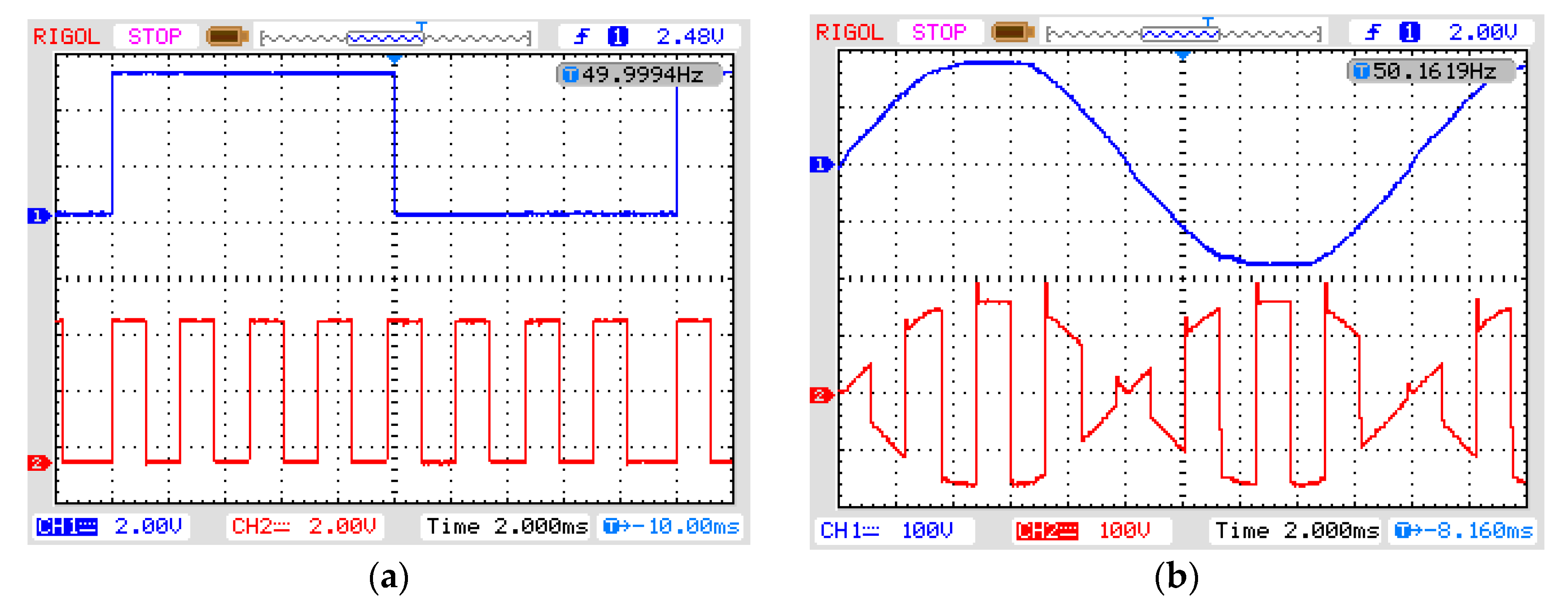
Figure 10a depicts the switching signal generated with ZCD so that it may be synchronized with the input voltage. It is generated by applying an interrupt to the Arduino once ZCD detects the positive zero crossings. In
Figure 10b, the output voltage is plotted with respect to the input voltage, while
Figure 10c determines the harmonics contents of the output voltage, where the dominant component exists at 400 Hz. The analysis of these figures depicts that the period of the output voltage is eight times lesser than that of the input voltage. Therefore, the output frequency is eight times greater than the frequency of the source voltage.
Figure 10d presents the input current waveform with respect to the input voltage. The input current is nearly sinusoidal, ensuring low harmonic contents and low THD. This ensures improvement in the input power factor.
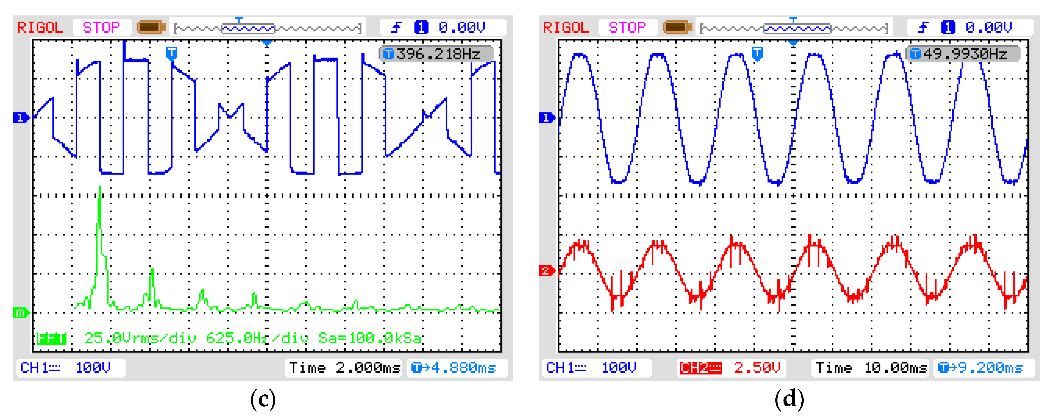
Figure 11a depicts the practically recorded waveforms of two complementary switching signals generated without zero-crossing detection. So, they are not synchronized with the input voltage. They are simply generated without any zero-crossing interrupt with any PWM generator. This characteristic simplifies the control effort significantly and reduces its complexity for the induction heating application. The analysis of
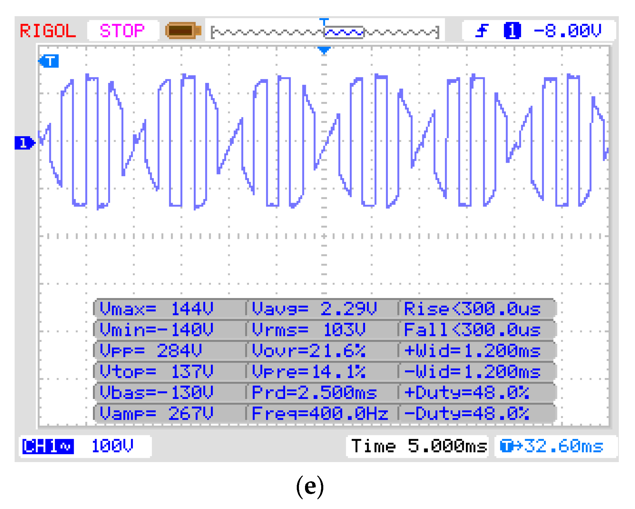
Figure 11b–d determines the power quality of the output voltage and input current. The rms value of the output voltage is recorded in
Figure 11e. This also validates the computed rms value of Equation (13) in
Section 1. The comparison of
Figure 10 and
Figure 11 depicts that the power quality characteristics of the output voltage and input current with and without zero-crossing detection are almost similar. This is true if output frequency is a few hundred times greater than that of the frequency of the source voltage. So, switching sequences can be directly generated and applied to the controlled switches. That is why the proposed topology is implemented without zero crossing detection for the induction heating application.
The nominal output frequency requirement in the domestic induction heating application lies in the range of 20 kHz to 100 kHz. The switching frequency of the converter is selected higher than the resonance frequency, so the effect of load equivalent inductance and capacitance should not reflect in the output and input currents. The resonance of the equivalent load inductance (40 µH), filtering inductor (1 mH), capacitance (1 µF), and resistance (120 Ω) is nearly 5 kHz. The switching sequence of 25 kHz is applied to the switching devices to obtain the output frequency of 25 kHz. This is achieved by operating the proposed converter 500 times in non-inverting and inverting modes in one cycle of the input voltage. That is why the output and input currents are in-phase with their corresponding voltage ensuring improved power quality.
Figure 12a shows the two complementary gating signals for 25 kHz switching frequency.
Figure 12b,c depicts the output voltage and current waveforms. The power quality of the input current is explored by plotting it with respect to the input voltage in
Figure 12d.
The envelope of the output voltage of
Figure 12b is equal and opposite to the instantaneous value of the input voltage.
Figure 12c is obtained by zooming the
Figure 12b around the peak value (150 V) of the input voltage to explore that the instantaneous value of the output voltage is equal to 150 V during non-inverting and −150 V during the inverting operation for positive input voltage. However, the rms values of the output and the input voltage are the same.
All the practically recorded waveforms of input currents (see
Figure 10,
Figure 11 and
Figure 12) have the same sinusoidal behavior ensuring low harmonic contents, low THD, and hence improved power factor. There is no voltage and current overshoot problem in output voltage, output, and input current. These characteristics of the proposed converter make it very attractive for the induction heating application.


 ,
, 


