1. Introduction
Broadband connectivity has become essential in everyday life both for business and for entertainment. This, together with the increasing demand of mobile connectivity in locations where terrestrial networks are not available or less efficient, has promoted the development of antennas to be installed on aircrafts, trains, boats and vans to provide interconnection via satellite.
Moving from experimental verification to operational conditions, aeronautical broadband services provided by satellites is today a reality; but to be commercially attractive, the services offered via satellite should have a quality comparable to those available via terrestrial networks, should allow the same type of applications and should be offered at an affordable cost.
Together with the technical issues to be addressed, a main driver is the cost, which comprises the cost of ground segment, which is related to materials, installation (mainly related to the antenna system) and maintenance of the equipment, the cost of the satellite segment and the overall operations of the system.
Focusing on the aeronautical platforms, satellite communication is the only means to provide continuous connectivity over the oceans. Airborne RF communication system applications pose challenging problems to current antenna technology:
Interactions with the aircraft aerodynamics impacting drag, lift and controllability;
Influence of the aircraft structure on the antenna performance;
Electromagnetic Compatibility (EMC)/Electromagnetic Interference (EMI) with other RF and/or electronic systems on board the aircraft;
Very wide-angle scanning performance, so as to operate at the extreme latitudes required by polar routes;
Compatibility with other satellite systems and with terrestrial communication services (involving beamwidths, beam pointing accuracy and sidelobes performance);
Keyhole problem typical of narrow beam antenna systems employing two axes for tracking a satellite. The keyhole is caused either by mechanical constraints or position slew rate limitations of the antenna mount [
1].
The ideal antenna should actually be high gain, broadband, low profile, highly reliable and low cost. Different choices of the antenna architecture [
2] could bring to a fully mechanical [
3], fully electronic [
4] or “hybrid” (mechanical–electronic) solutions [
5,
6].
The fully mechanical and hybrid solutions are based on antennas with rectangular or highly elliptical apertures in order to minimize the antenna thickness. They create highly elliptical beams and, because they rely usually only on two motors, it is not always possible to project the most directive cut of the pattern along the equatorial plane. The addition of a third axis permits limiting this keyhole problem. Solutions based on fully electronic steering solve the keyhole issue and permit to maintain a transmit–receive link also when flying near the Equator where respecting the regulatory aspects is particularly challenging. Moreover, the fully electronic antenna, thanks to the graceful degradation (typical of active arrays) exhibits lower costs in terms of maintenance as compared to mechanically steering antennas. Electronically scanning antennas can be flat or conformal. In this development conformal antenna are considered in order to guarantee equalized performances in an entire half sphere. It is important to mention that by limiting the scanning directions with respect to the zenith within a cone with an angular opening of 60 degrees instead of 90 degrees, the antenna thickness could be reduced by a factor of two.
2. Antenna Requirements
The main requirements for the Ku-band aeronautical market, in terms of antenna characteristics, are summarized in
Table 1.
The operational band is the complete Ku-Band (10.7 ‒ 12.75 GHz in receive and 14.0 ‒ 14.5 GHz in transmit). The realignment of the polarization in respect to the satellite for both receiver and transmit signals, with the capability to operate also with the circular polarization in receiver mode, is required.
The minimum antenna requirements in terms of operative field of view (e.g., antenna gain-to-noise temperature [G/T] over RF band in the entire field of view and for every selectable polarization, Equivalent Isotropic Radiated Power [EIRP] over RF band in the entire field of view and cross-polar discrimination (including pointing error)) are reported in the
Table 2.
It has to be underlined that an antenna in transmission mode has to respect the applicable regulations [
7] for the EIRP antenna patterns expressed in terms of power density per bandwidth as shown in
Figure 1.
Moreover, complexity and cost of the antenna are other key factors to take into account together with practical feasibility and ability to operate simultaneously in receiver and transmit modes.
3. Antenna Design
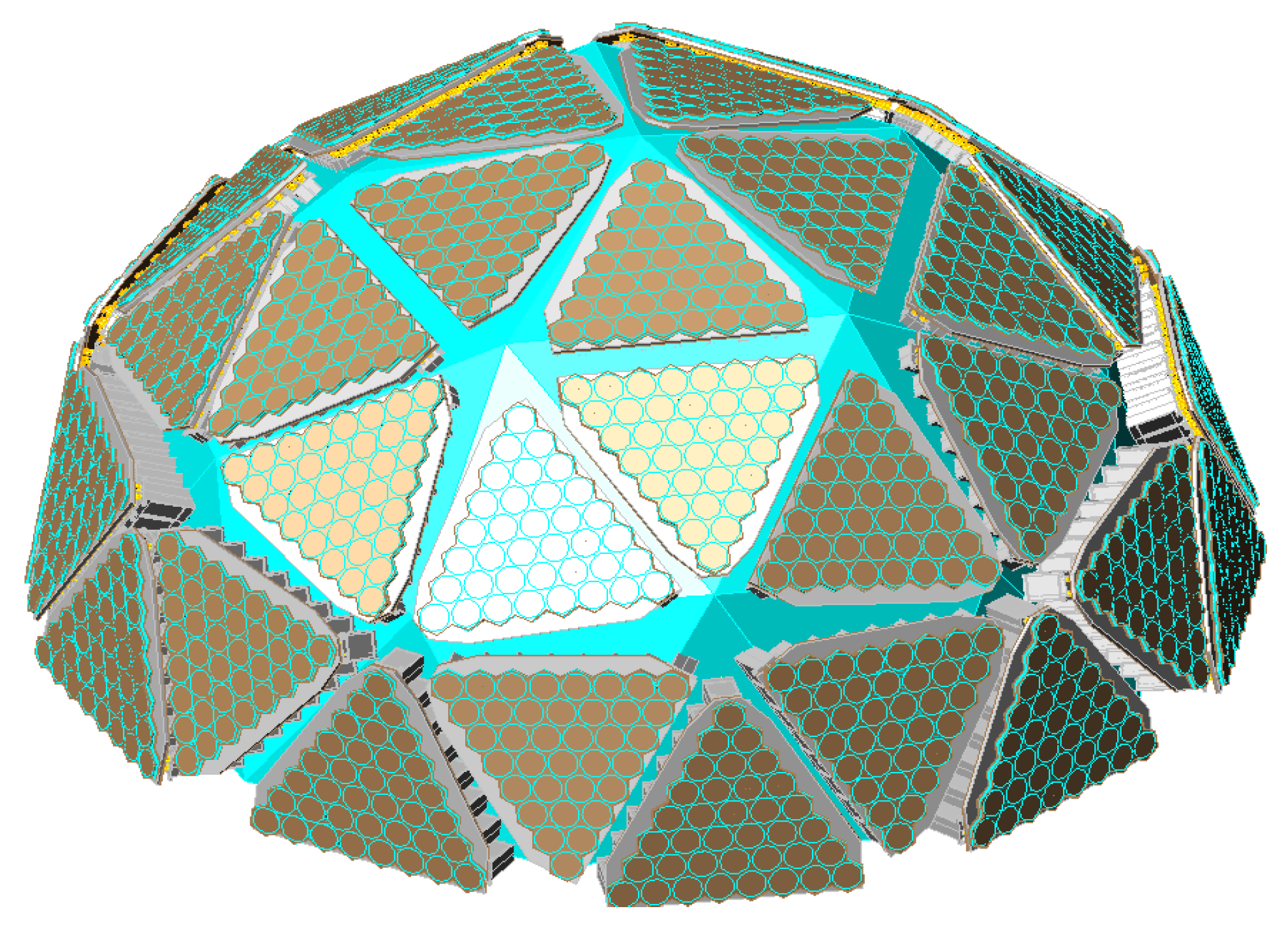
The hemi-spherical antenna array when mounted on the aircraft is able to guarantee the proper link, whatever the position of the airborne with respect to the satellite is, thanks to its shape [
8]. In order to minimize the complexity of the antenna, the hemi-spherical continuous surface has been approximated with flat facets. To replace the sphere, the icosahedrons, a polyhedron with twenty equilateral triangles, has been selected as starting geometry. Then a new solid of 80 facets has been generated; where, to the original vertexes, the points of middle edge of each triangle have been added after the projection on the sphere surface. Half portion of the new solid is covered by sub-arrays and, after further refinements, the position of the tile is adjusted to avoid the intersection of the extruded part which contains the RF components and the control logic. As a result of the optimization, the geodesic hemi-sphere with 40 facets shown in
Figure 2 has been selected as antenna aperture. Each triangular face is composed by the same sub-array, i.e., the same number of radiating elements arranged in a triangular lattice.
The final optimized antenna is able to combine on the same aperture the receiver and transmitter capabilities, has a diameter of 84 cm, a height of 39 cm and a weight in the order of 90 Kg. The number of radiating elements is 1440 with an inter-spacing of 22 mm, which corresponds to one wavelength in the transmit higher frequency. Each triangular sub-array, indicated as tile, presents 36 radiating elements.
For a fixed beam direction, only a sector composed by 14 tiles is active while all the other elements are turned off. All the radiating elements in the active sector are excited in order to generate an equi-phase wave front perpendicular to the desired beam direction.
It is important to note that when projecting the conformal aperture in an arbitrary pointing direction, the triangles are deformed and become irregular; this concept is clear watching at
Figure 2. The resulting sparse array, thanks to this irregular lattice, exhibits a pattern without grating lobes. Moreover, the optimization of the excitation coefficients in amplitude and phase, or in phase only, permits to maintain the side lobes within the spectral density mask imposed by the regulatory aspects as demonstrated in the paper.
Concerning the antenna electrical architecture, the input/output ports are fed with the IF band signal, and converted in a Ku band signal by the up/down converter. Each tile is composed by the radiating elements and the transmit/receive modules, directly connected on the back. Two dedicated beam forming networks 1:40 for the receiver and the transmitter mode are connected to the tiles and the CPU controls a set of switches in order to involve the selected sub-arrays to form the antenna beam. The CPU controls the beam steering and the polarization alignment.
The tracking capability of the antenna permits to point the beam electronically in a hemi-spherical field of view (i.e., 360 degrees in azimuth and 90 degrees in elevation) with negligible degradations of the electrical performance, guaranteeing a minimum G/T of 8 dB/K-1 and an EIRP of 43 dBW.
The results obtained using the simulated pattern of an embedded radiating element are reported in the following. The excitation coefficients have been optimized considering the realistic functionality of the Receive(Rx)/Transmit(Tx) active module (combining the amplitude and phase of the two orthogonal polarization for each radiating element).
The G/T result is shown in
Figure 3a. The performance matches the required 8 dB/K in the entire field of view. As expected, the degradation of the performance at lower pointing angles is due to the different orientation angles of the tiles, which are involved in the beam forming, with respect to the horizon.
The typical azimuth receiver antenna pattern is shown in
Figure 3b. During the transmission, all the active devices are able to work at the maximum power level and the expected performance in term of EIRP are reported
Figure 4: The minimum guaranteed value is in the order of 43 dBW over the complete antenna field of view.
The antenna is also able to control the transmit antenna patterns side-lobe in order to respect the applicable regulatory recommendations such as ETSI in the European countries [
7] and the FCC in the United States.
The typical azimuth transmit antenna pattern is reported in
Figure 5a. The black line represents the mask that has been imposed in the optimization process (corresponding to the ETSI mask for 512 KHz bandwidth). The corresponding elevation transmit antenna pattern is shown in
Figure 5b.
4. Developed Devices
The main challenges in the design of the antenna have been: (a) the development of the radiating element, (b) the development of the active module for transmitter/receiver and (c) the design and manufacturing of a digital vector modulator (DVM) able to integrate in a single chip the attenuator and phase shifter features. These three components are described in the following paragraphs.
4.1. Self-Diplexing Radiating Element Design
The first criticality in the design of Tx/Rx radiators is the capability to separate the transmitted signal from the received one. A typical approach consists in designing a radiating element covering the entire band and then connecting a diplexer or a circulator. However, this configuration has the drawback to increase the overall dimensions and the ohmic losses at the Low Noise Amplifier (LNA) input.
A more efficient solution consists of implementing, for each radiating element, two different ports: One for Tx and one for Rx signal. This type of configuration is called a self-diplexing solution. This approach offers better electrical performance and permits the reduction of the manufacturing complexity.
The radiating element is realized using two different substrates of RT/Duroid 5880 with 0.508 mm thickness separated by a foam with 1 mm thickness.
Starting from the ground, the first two metallizations are dedicated to the receive capabilities: The first patch has a diameter of 8.5 mm and it is fed by a UT047 coaxial cable; while the second patch, with a diameter of 10.4 mm, implements the stacked configuration, by the foam spacer, that allows to operate over the large frequency band. The transmit radiating configuration uses a single patch of 7.4 mm diameter and it is fed directly by UT047 coaxial cable taking advantage of the upper receive metallization for the ground. The
Figure 6a shows a sketch of the self-diplexing radiating element assembly; while in
Figure 6b the 3D model used in full wave analysis is shown.
The radiating element provides four ports able to operate in dual linear orthogonal polarizations both for transmission and reception.
A prototype of the radiating element is shown in
Figure 7a, while the engineered radiator is shown in
Figure 7b. The hexagonal ground makes support functionality and it circumscribes a circle of 22 mm of diameter.
Return loss at Rx and Tx ports and isolation are reported in
Figure 8 and
Figure 9, respectively. It is important to note that the isolation between the Rx and Tx ports over the entire Tx band is better than 20 dB.
The gain for the Rx and Tx radiating elements have been measured vs. frequency. The results are reported in
Figure 10a,b. The gain in free space condition is better than 8 dB for the receive ports over the frequency band with VSWR of 2:1; while at transmit ports 7 dB gain are guaranteed.
In
Figure 11, the measured radiation patterns of the radiating element in free space configuration are reported for the extreme frequencies of the operating receive band, while for the transmitting band it shows the central frequency in the same conditions. The reported measured radiation patterns are compared with the simulation analysis results demonstrating an excellent agreement.
4.2. Transmit/Receive Active Module Design
Each radiating element is directly connected with an active circuitry that provides the functionality of the Tx/Rx module. The Tx/Rx module (intellectual property of Airbus Italy [
9]) is able to realign the linear polarization in receive and in transmit or, alternatively, may allow the generation of a circular polarization. The phase shifters used for the polarization control are also able, at the same time, to form the antenna beam imposing the correct relative phase delay between the elements. The active modules are composed by the receive device and the transmit device (the assembled Tx/Rx device is shown in
Figure 12).
The manufactured modules are presented in
Figure 13: In particular, the control board sides are shown. Their dimensions are 20.6 by 7 by 37 mm
3, with a weight of 15 g.
Figure 14a shows the channel gain behavior vs. the frequency when the attenuator and the phase shifter are set at the nominal value (zero).
Figure 14b shows how all the SSPAs (Solid State Power Amplifier) power is moved between the two output ports when the relative phase between the two channels is properly set: The correct rotation of the linear polarization is provided by the opportunely balanced power.
4.3. Digital Vector Modulator (DVM)
A DVM in Ku band to control in amplitude and phase the radiating elements has been designed, manufactured and tested. It consists of a MMIC (Monolithic Microwave Integrated Circuit) in GaAs (Gallium Arsenide) technology integrating a 5-bit attenuator (ATT), a 5-bit phase shifter (PS) and a serial to parallel converter (S2P), as reported in
Figure 15.
The DVM development allows to realize T/R Modules in Ku band with mechanical dimensions and interconnections reduced with respect to that available on the market, i.e., separated digital attenuator and phase shifter (
Figure 16).
To realize a S2P on GaAs technology the E-mode and the D-mode transistors should be realized on the same wafer. To do this, the TQPED (MMIC technological process) process has been selected. A 10 bit S2P has been customized by TriQuint in line with Airbus Italy requirements summarized in
Table 3.
Each attenuator and phase shifter cell have been designed separately. The position of the cells in the MMIC chain has been properly chosen considering the RF performances and the layout arrangement.
The DVM MMIC and the stand alone main block have been manufactured on a 5 by 10 mm
2 tile in a multi project wafer (MPW). The manufactured MMIC has been mounted on an aluminum carrier and tested by means of a probe station. The pictures of the DVM under microscope is reported in
Figure 17.
The RF measurements are hereafter provided: Relative amplitude and phase variations (
Figure 18), measured insertion loss with only phase shifter variation and phase error due to the attenuation states (
Figure 19), return loss port 1 and return loss port 2 (
Figure 20).
The performances of the 11.25°, 90° and 180° phase shifter cells in the DVM MMIC were very good in terms of relative phase shift: An average error of 1° has been measured. Vice versa, the measurement of the 22.5° and 45° cells shows a phase shift higher than the target value (8° and 4°, respectively). It has to be highlighted that the phase errors of the 22.5° and 45° cells in the stand alone main blocks is the half respect the same cells inside the DVM MMIC.
The performance of the attenuator cells agree with the expected ones, except for the phase stability vs. gain variation in Tx band which presented an undesired phase shift for attenuation higher than 17.25 dB. However, such deviation for the specific parameter is generally also present in commercial devices and is not considered significant for the specific project.
The insertion loss of the reference state was about 11.2 dB and flat in band. Considering the combination of the two COTS (Commercial of-the-shelf) component employed in the antenna demonstrator we experienced an overall insertion loss of 13 dB. Taking into account the inductive effect of the wire bonding interconnections, the return losses of both ports are below 10 dB.
Finally, the power consumption of the S2P, designed by TriQuint, was 250 mW. This could be drastically reduced (up to 120 mW) with the implementation of some identified technical solutions.
5. Test Campaign Results
The activity has been finalized with an exhaustive test campaign dedicated to evaluate first, the performance of the single radiating element in active configuration (
Figure 21), second, considering it as a demonstrator of a linear sub-array of 5 active radiating elements embedded within the complete tile composed by 36 dummy radiators in triangular lattice (
Figure 22).
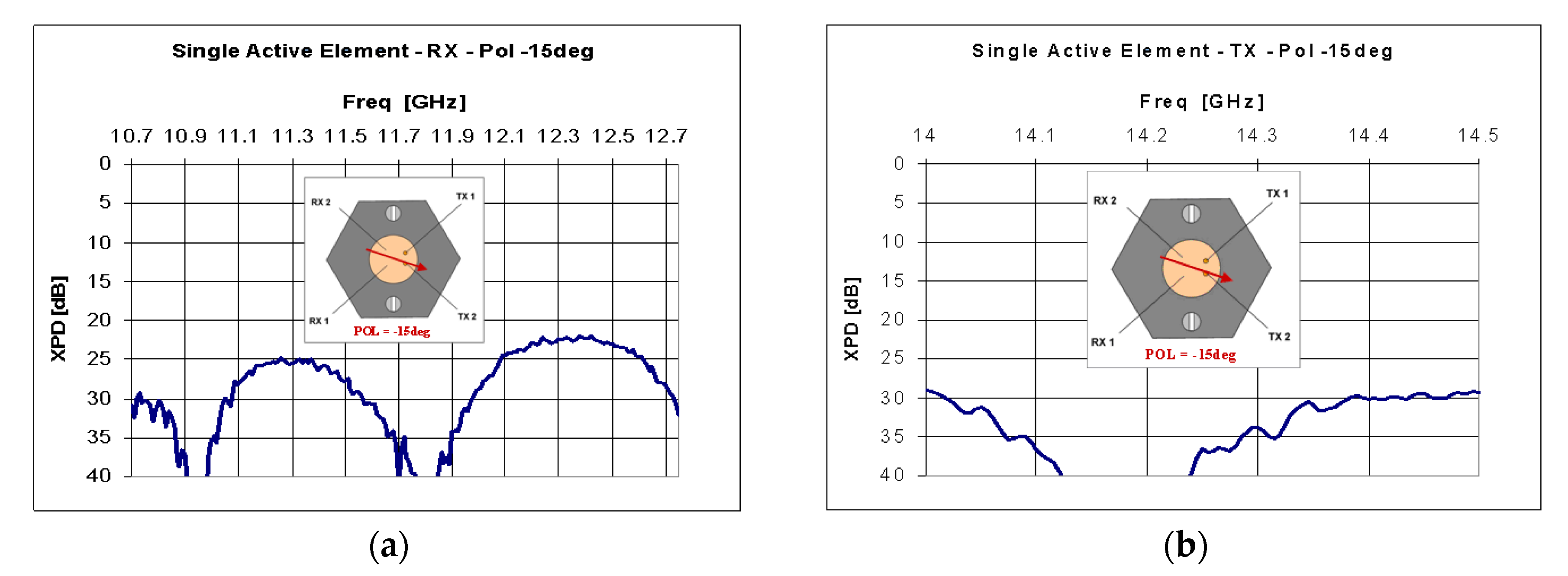
The radiation pattern of the active radiating element in free space configuration have been measured in several cases where the impinging RF wave in linear polarization was characterized by a defined alignment angle with respect to the radiating element axes. Setting the proper amplitude and phase coefficients, the active radiating element was able to align correctly the received polarization providing a very good discrimination between the two orthogonal polarizations.
Figure 23a reports the received cross polar component over the complete operating band, when the attenuator and the phase shifter controls are correctly set for a copolar signal with the polarization rotated by 155 degrees; while
Figure 23b shows the same behavior for the transmit channel over the entire frequency band.
Figure 24a shows the measured radiation pattern in receive when a misalignment of 30 degrees has been corrected by the Tx/Rx Active Module.
The same performance has been provided for the active radiating element operating in transmit mode:
Figure 24b shows an example of radiation pattern for a transmitted polarization rotated of 15 degrees with respect to the nominal axes.
Figure 22 shows the manufactured antenna demonstrator which implements the triangular array geometry in the real dimensions and representing the tile of the hemi-spherical phased array shown in
Figure 2. A subset composed of five radiating elements is connected to the Tx/Rx active modules and the radiation pattern has been measured for different beam steering positions and polarization alignments.
Figure 25a shows the measured radiation pattern when the excitation coefficients have been applied to steer the beam at 10 degrees without the recovery of a polarization misalignment (30 degrees); while in
Figure 25b it reported the same measurement but with the recovery of the polarization angle.
Figure 26 shows the measured radiation pattern in transmit mode when the excitation coefficients are applied to provide the beam steering of −10 degrees and a polarization rotation of 30 degrees.
6. Conclusions
The reported technological solutions constitute the base of on-going developments for affordable phased-array antennas for commercial aeronautical satellite communications. Similar developments are currently ongoing at Airbus Italy targeting higher frequencies (i.e., Ka-band) as well as space-borne phased-arrays.

 ,
, 


