Abstract
We present a low-power CMOS active-resistance-capacitance (active-RC) complex bandpass filter (BPF) with tunable gain, bandwidth, center frequency, quality factor, and passband flatness for Bluetooth applications. A transfer function analysis for a cross-coupled Tow-Thomas biquad structure is presented to prove that the flatness profile of the passband gain can be effectively controlled by independently tuning two cross-coupling resistors. The proposed biquad-based complex BPF was employed to realize a fourth-order baseband analog processor for a low intermediate frequency (low-IF) RF receiver. The baseband analog processor was composed of two complex biquad filters and three first-order variable-gain amplifiers. It was fabricated in a 65-nm RF CMOS and achieved wide tuning capabilities, such as a gain of −15.6 to 50.6 dB, a bandwidth of 1.4–3.9 MHz, a center frequency of 1.5–4.1 MHz, and a passband flatness of −1 to 1 dB. It also achieved an image rejection ratio of 40.3–53.3 dB across the entire gain tuning range. It consumed 1.4 mA from a 1 V supply and occupied an area of 0.19 mm2 on the silicon substrate. The implementation results prove that the proposed complex BPF was able to effectively enhance the signal processing performances through the flexible and wide-range tunability of the passband flatness, as well as that of the gain, bandwidth, center frequency, and quality factor.
1. Introduction
Bluetooth low energy (BLE) is a wireless communication technology for Internet-of-things (IoT) applications that operates in the 2.4 GHz industrial scientific and medical (ISM) band. The low intermediate frequency (low-IF) receiver architecture is widely adopted for CMOS RF receivers in BLE applications because it can cope with flicker noise and dc offset issues more effectively than zero-IF architecture. For low-IF RF receivers, analog complex bandpass filters (BPFs) are needed for appropriate complex-domain baseband channel selection and filtering [1,2]. The complex filter allows only the positive frequency bands to pass and suppresses the negative frequency bands. Complex BPFs are usually realized by interconnecting two real-domain low-pass filters (LPFs) placed in in-phase and quadrature-phase (I/Q) paths via some cross-coupling impedance components [3].
Many low-power CMOS complex BPFs have been reported for low-power wireless applications [2,4,5,6,7,8,9]. To ensure a good sensitivity in the RF receiver, the complex BPF employed is desired to have tunable bandwidth, quality (Q) factor, and gain, as illustrated in Figure 1a−c. The bandwidth tuning (as shown in Figure 1a) is needed for faithful compliance to a standard-specified channel bandwidth or the flexible support of several multi-mode bandwidths. The tuning of the Q-factor, as shown in Figure 1b, allows the precise adjustment of the band-edge peaking profile. By tuning the gain (as shown in Figure 1c), the BPF can effectively deal with wide variations of the received signal strength. Hence, most of the previous complex BPFs were designed to allow the tuning of the three parameters or part of them [2,4,5,6,7,8,9]. The bandwidth tuning can be found in [4,5,6,9], and center frequency tuning can be found in [4,5,9]. Balankutty et al. [2] reported a complex BPF with the gain, bandwidth, center frequency, and Q tuning, as well as a simple reconfigurability to a real-domain LPF.
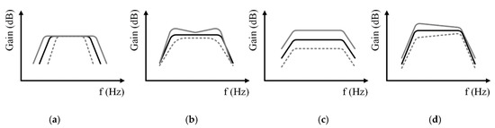
Figure 1.
Filter parameter tuning characteristics: (a) bandwidth, (b) quality factor, (c) gain, and (d) passband flatness.
Nevertheless, most previous complex BPFs [2,4,5,6,7,8,9] have not allowed the tuning of passband gain flatness (illustrated in Figure 1d), which is an important performance parameter in the analog baseband filter. A flat gain profile in the passband is essential to minimizing the amplitude distortion of the processed signal. It is interesting to note that Wu and Chiu [10] reported an active-resistance-capacitance (active-RC) real-domain BPF—although it was not a complex BPF—with measurement results for the in-band flatness deviation, but never implemented its tunability. Lee et al. [11] and Gomez-Garcia et al. [12] proposed a design method to improve the passband flatness, but it was limited only to passive-type real-domain BPFs.
In [7], we reported preliminary circuit design results of a complex BPF for BLE [1] and MedRadio [13] applications, but did not realize the passband flatness tuning capability. In this work, we present a low-power complex BPF with a tunable in-band gain flatness, gain, bandwidth, center frequency, and Q-factor. A transfer function analysis is carried out to prove the passband flatness tuning mechanism in a biquad-based complex BPF. Circuit design and implementation results in CMOS are presented to demonstrate the circuit performances.
2. Circuit Design
Figure 2 shows the circuit diagram of the proposed biquad-based complex BPF, which exhibits second-order complex bandpass filtering characteristics. As shown in the figure, the complex BPF comprises two biquads in the I and Q paths that are cross-connected by two cross-coupling resistors Rxa and Rxb. The biquad is based on a two-integrator-loop Tow-Thomas structure, which is widely adopted for baseband LPF designs [14,15]. The biquad in Figure 2 is known as an inverted Tow-Thomas structure since its lossless integrator part is placed before the lossy integrator part [16].
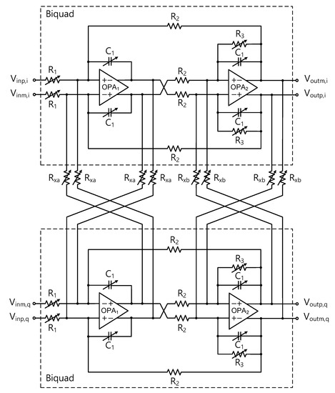
Figure 2.
Circuit diagram of the proposed complex filter.
In the rest of this section, we describe the transfer function analysis of the complex BPF. The transfer function of the unit biquad (indicated by dashed box in Figure 2) is expressed in Equation (1). The LPF has a cutoff frequency fc = 1/(2πC1R2), quality factor Q = R3/R2, and gain Av = R2/R1. As indicated in Figure 2, the passive components R1, R3, and C1 are designed in a switched array form so that their values can be digitally tuned [14]. R2 is set to a fixed value because changes in this value lead to simultaneous changes of the cutoff frequency, quality factor, and gain.
Figure 3 shows that shifting up the LPF response by a constant frequency value fo will transform the original LPF response to a desired complex BPF response. The resulting transfer function is obtained by substituting s with s − jωo in Equation (1), and written as Equation (2). Equation (2) indicates that the gain at the image-band when s = −ωo is much lower than the gain at the desired-band when s = +ωo, and thus the desired image rejection can be obtained by the complex BPF.
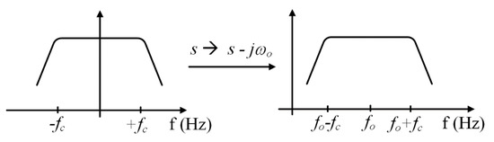
Figure 3.
Illustration of pole shifting in the complex domain.
The frequency shifting operation can be realized by cross-coupling the I and Q path signals via the two cross-coupling resistors for the lossless OPA1 and lossy OPA2 integrators, which are denoted by Rxa and Rxb, respectively (Figure 2). The frequency shift value ωo of the complex BPF is determined by the time constant involved with the cross-coupling resistors and its corresponding capacitors. It is interesting to note that the complex BPFs reported in [4,6] had the same value for Rxa and Rxb, whereas those reported in [2,5] had different values for Rxa and Rxb. Nevertheless, their designs were aimed at equalizing the time constants and, consequently, the frequency shift values involved with Rxa and Rxb. However, the effect of setting Rxa and Rxb and their corresponding time constants to different values on the frequency response of the complex BPF have not been reported. In this work, we set the two cross-coupling resistors Rxa and Rxb and their corresponding time constants to different values to observe their impact on the frequency response of the complex BPF.
To understand the effects of Rxa and Rxb on the passband flatness and other performance parameters such as gain, bandwidth, and center frequency, a transfer function analysis that is more accurate than Equation (2) is needed. This can be obtained by including the effects of different values of Rxa and Rxb. Figure 4 shows the circuit diagram of an I-path biquad filter, redrawn from Figure 2 after simplifications. The differential signaling is converted to a single-ended form, the imaginary signals fed from the Q-path part are expressed as jVx and jVout, and the phase inversion is simply expressed by a negative unity gain buffer. Equations (3) and (4) are obtained by applying Kirchhoff’s current law at the I/Q-path joint nodes A and B in Figure 4. By combining Equations (3) and (4), the total transfer function of the complex BPF, HCBPF(s), can be obtained as Equation (5).
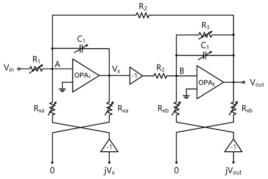
Figure 4.
Complex filter modeled in a single I/O structure.
With ωoa = 1/(RxaC1) and ωob = 1/(RxbC1), Equation (5) can be rearranged to take a form similar to that of Equation (2):
Compared to the transfer function given in Equation (2), which assumes a single frequency shift value of jωo, Equation (6) indicates that jωo can be seen as split into the two different values jωoa and jωob in the s2 term of the denominator, while it can be seen as jωoa in the s term. Note that, in practice, the difference between Rxa and Rxb, as well between jωoa and jωob, should not be too large, but small enough so that only a narrow range tuning of Rxa and Rxb should be sufficient for fine adjustment of the gain flatness.
We compare the magnitudes of HCBPF(s) of Equation (6) at s = jωoa and jωob. Equations (7) and (8) are the expressions for |HCBPF(jωoa)| and |HCBPF(jωob)|, respectively. It is interesting to note that |HCBPF(jωoa)| is always greater than |HCBPF(jωob)|, while they are the same when Rxa = Rxb, as observed in the conventional design represented by Equation (2).
We examine the impact of different values of |HCBPF(s)| at s = jωoa and jωob on the passband flatness. Figure 5 shows three possible cases where the two frequency shift values foa and fob are given by 1/(2πRxaC1) and 1/(2πRxbC1), respectively. First, Figure 5a shows the conventional design when Rxa = Rxb, where foa and fob are the same. Figure 5b,c shows that different values of Rxa and Rxb lead to different values of foa and fob, respectively. Because |HCBPF(s)| is always higher at s = jωoa than at s = jωob, as implied by Equations (7) and (8), the passband gain profile should always be slanted up from fob toward foa. Therefore, Rxa and Rxb can be tuned to adjust the passband gain profile flatness. Meanwhile, it should be pointed out that simply equalizing Rxa and Rxb cannot guarantee a perfectly flat passband in practice, owing to the variability and non-uniformity of the CMOS fabrication process. Therefore, some level of independent tuning of Rxa and Rxb as proposed in this work is instrumental in CMOS implementations of the complex BPFs.
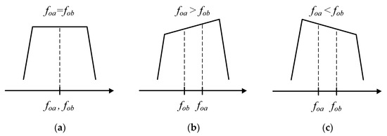
Figure 5.
Passband flatness control: (a) foa = fob, (b) foa > fob, (c) foa < fob.
The passband flatness tunability via Rxa and Rxb is verified by the numerical computation of the transfer function given in Equation (5). Figure 6 shows the computed gain characteristic curves with Rxa and Rxb set in the range of 45–65 kΩ and R1 = 50 kΩ, R2 = 82 kΩ, R3 = 58 kΩ, and C1 = 1.5 pF. As can be seen, when Rxb is greater than Rxa, the passband gain profile becomes slanted up toward the high frequency region, as also indicated by Figure 5b. Further, when Rxa is greater than Rxb, the passband gain profile becomes slanted down toward the high frequency region, as also indicated by Figure 5c. When Rxa and Rxb are both set to 55 kΩ, the passband gain profile shows very flat characteristics. However, as discussed above, such a perfect flat condition would never occur after practical CMOS implementations due to the process variability and non-uniformity. Thus, the independent tuning scheme of Rxa and Rxb should be very effective to improving the passband gain profile flatness.
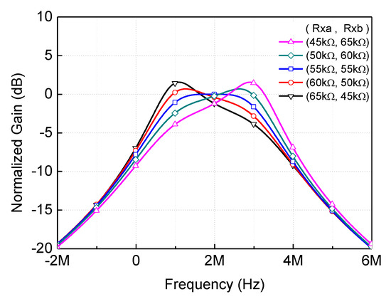
Figure 6.
Computed passband gain profiles.
We designed a fourth-order baseband analog processor by employing the proposed complex BPF. The block diagram is shown in Figure 7. It is designed to perform complex bandpass filtering and amplification for a BLE low-IF RF receiver. Considering the BLE standard specifications [17], the passband bandwidth is designed to cover 2 MHz, and its center frequency is simultaneously tuned to the same value of the bandwidth. The baseband analog processor is composed of two complex BPFs and three variable-gain amplifiers. The three variable-gain amplifiers and two biquads are placed alternately to maximize the overall dynamic range and sensitivity. Because the total baseband analog processor employs two complex biquad-based BPFs, it has fourth-order Butterworth bandpass filtering characteristic with image rejection at the negative frequency band. On-chip dc-blocking capacitors Cb of 10 pF are used to remove dc components, as the desired band resides in the low IF region away from dc. The variable-gain amplifier is designed in a conventional inverting amplifier structure. The gain control ranges of the first, second, and third variable-gain amplifiers are 0–12 dB with a 6 dB step, −3–9 dB with a 3 dB step, and −9–9 dB with a 3 dB step, respectively. The corner frequencies of the variable-gain amplifiers are set to 8 MHz, which is wide enough not to alter the overall BPF bandwidth. The complex BPF has a gain tuning range of −2 to 10 dB. The total gain control range of the full baseband analog process is +66 dB, from −16 to 50 dB.
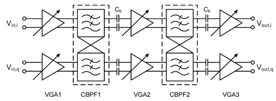
Figure 7.
Block diagram of the baseband analog processor.
A total of 14 operational amplifiers are used for the total baseband analog processor shown in Figure 7. Figure 8 shows the circuit diagram of a unit operational amplifier, which is a fully differential two-stage amplifier with a common-mode feedback for dc-level stabilization. The operational amplifier dissipates approximately 100 μA on average (the actual current dissipations of the 14 operational amplifiers were optimized separately and ranged from 80 to 110 μA), for which 40 μA is dissipated by the input differential pair M1,2, 45 μA is dissipated for the common-source stage M5,6, 10 μA is dissipated for the common-mode feedback stage M11,12, and 5 μA is dissipated for the biasing current mirror stage M15. Simulations show that the opamp has an open-loop gain of 56.2 dB, a gain bandwidth product of 80.4 MHz, and a phase margin greater than 87.6° for the differential and common modes. The frequency compensation components are Rc = 2 kΩ, Cc = 900 fF, Rf = 410 kΩ, and Cf = 200 fF.
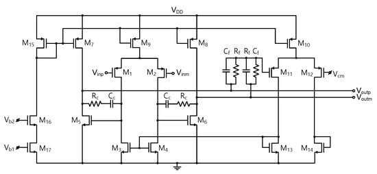
Figure 8.
Circuit schematic of the operational amplifier.
3. Implementation Results
The baseband analog processor shown in Figure 7 was fabricated in a 65nm RF CMOS process. Figure 9a,b shows the layout and micrograph of the fabricated chip. The total active area excluding the pad and electrostatic discharge cell frame is 750 × 250 µm2. The fabricated circuit was tested after mounting and wire-bonding directly on a printed circuit board. The internal digital register values of the circuit were controlled using a serial peripheral interface. With a 1 V supply, the total current dissipation was found to be 1.4 mA, which originated from the 14 operational amplifiers as well as the additional biasing blocks. It should be pointed out that the total current dissipation of this circuit did not change at all for all the bandwidth, center frequency, Q, and passband flatness tuning conditions. The layout symmetry in the differential signal path and the I/Q path was maintained as high as possible to minimize the unwanted degradation of the image rejection and I/Q signal mismatch.
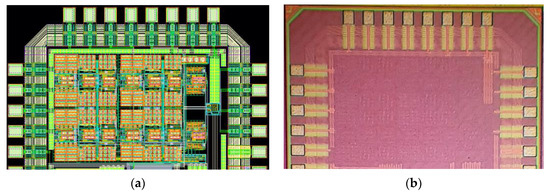
Figure 9.
The fabricated analog baseband processor: (a) layout and (b) micrograph.
The filter tuning characteristics were tested by applying single-tone I/Q signals at the input by using a signal generator, and measuring the output spectrum at the output by using a spectrum analyzer. Figure 10a,b shows the bandwidth tuning characteristics obtained from simulations and measurements, respectively. As shown in the figures, the simulation and measurement results are in good agreement. The bandwidth tuning was performed by 4-bit C1 tuning from 0.787 to 2.1 pF and resulted in 16 curves. As shown in Figure 10b, the tuning ranges of the bandwidth and center frequency were 1.4–3.9 and 1.5–4.1 MHz, respectively. These results confirm that the center frequency can be set to the same value as that of the bandwidth, as required by typical BLE low-IF receivers.
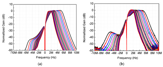
Figure 10.
Bandwidth tuning characteristics obtained by (a) simulations and (b) measurements.
Figure 11a,b shows the gain tuning characteristics obtained from simulations and measurements, respectively. The figures show that, in total, there were 23 digitally controlled gain curves with the center frequency and bandwidth both set to the nominal value of 2 MHz, as required by the BLE standard [17]. The gain control range was −15.6 to 50.6 dB, and excellent agreements were observed between the simulation and measurement results. Figure 11 also demonstrates the image rejection performances by simultaneously showing gain characteristics at the negative and positive frequency regions. The actual measurements for the negative frequency region characteristics were performed by exchanging the I and Q path signal phases. The image rejection ratio was evaluated by comparing the gains at a given center frequency and at its negative counterpart. Thus, when the center frequency and bandwidth were set to 2 MHz, the two gain values at +2 and −2 MHz provided the image rejection ratio. Figure 12 shows a particular measured spectrum demonstrating the image signal rejection. The higher and lower tones represent the desired signal at +2 MHz and the image signal at −2 MHz, respectively. An image rejection of 53 dBc can be observed. The image rejection performances over the total gain tuning ranges were found to be 40.3–53.3 dBc.
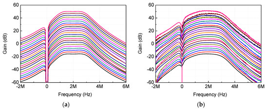
Figure 11.
Gain tuning and image rejection characteristics obtained by (a) simulations and (b) measurements.
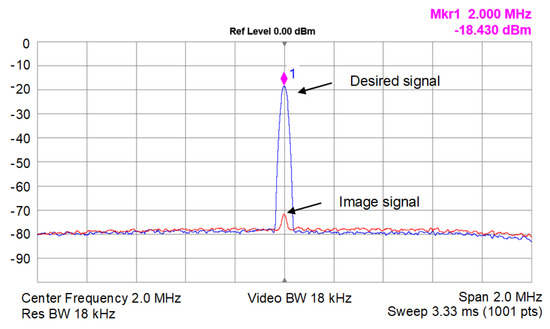
Figure 12.
Measured image rejection ratio.
Figure 13a,b shows the passband gain flatness tuning results obtained by simulations and measurements, respectively, with the results in excellent agreement. The bandwidth and center frequency were set to the nominal value of 2 MHz. Five gain profile curves are shown in the figure with Rxb tuned in five steps of 40, 43, 48, 52, and 55 kΩ, and Rxa fixed to 52 kΩ. It should be pointed out that the actual tuning resolutions of Rxa and Rxb were designed as 3- and 4-bit, respectively, so that much finer tuning than Figure 13 was possible when needed in practice. It can be observed that the gain difference at the low- and high-end cutoff frequencies could be tuned from −1.0 to +1.0 dB. In addition, as verified by the analytic and computational results in Section 2, we found that as Rxb increased, the passband gain profile gradually changed from being slanted downward to upward. These results imply that when the passband gain flatness is not satisfactory after CMOS implementation because of possible process variability and non-uniformity, the passband gain profile can be finely adjusted for maximal flatness by on-chip tuning.
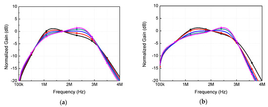
Figure 13.
Passband gain flatness tuning characteristics obtained by (a) simulations and (b) measurements.
The evaluated performances are summarized and compared with those of recently reported complex BPFs, and the results are shown in Table 1. The results demonstrate that the proposed baseband analog processor had a very wide tuning capability of the gain, bandwidth, and center frequency. Moreover, to the best of our knowledge, it was the first to support passband gain flatness tuning. The wide and flexible tuning capabilities of the gain, bandwidth, center frequency, and passband flatness of this baseband analog processor were expected to allow high selectivity and sensitivity performance in low-power CMOS low-IF RF receivers for BLE applications.

Table 1.
Performance summary and comparison.
4. Conclusions
Through transfer function analysis and computational verifications, we showed that the passband gain flatness profile of a biquad-structure complex BPF could be effectively controlled by independently controlling two cross-coupling resistors. With the biquad-structure complex BPF, we implemented a fourth-order Butterworth-type complex-bandpass-filtering baseband analog processor for BLE applications. The baseband analog processor was designed in a 65 nm RF CMOS and exhibited flexible and wide-range tuning capability at gains of −15.6 to 50.6 dB, bandwidths of 1.4–3.9 MHz, center frequencies of 1.5–4.1 MHz, and a passband flatness of −1 to 1 dB. Image rejection ratios of 40.3–53.3 dB were observed. The proposed CMOS design of the complex BPF could be employed to develop high-performance low-IF RF receivers for BLE and IoT applications.
Author Contributions
Conceptualization, J.K., S.C., and H.S.; validation, J.K., Y.L., and S.C.; data curation, J.K.; investigation, J.K. and H.S.; writing, J.K. and H.S.; visualization, J.K. and H.S.; supervision, H.S. All authors participated for all other aspects. All authors have read and agreed to the published version of the manuscript.
Funding
This work was supported by the Industry, Academy, and Research Institute New Business R&D Voucher Project (S2778811), the Institute for Information and Communications Technology Planning and Evaluation (2018-0-00712), and the Korea National Research Foundation (2020R1A2C1008484).
Conflicts of Interest
The authors declare no conflict of interest.
References
- Prummel, J.; Papamichail, M.; Willms, J.; Todi, R.; Aartsen, W.; Kruiskamp, W.; Haanstra, J.; Opbroek, E.; Rievers, S.; Seesink, P.; et al. A 10 mW Bluetooth Low-Energy Transceiver with On-Chip Matching. IEEE J. Solid-State Circuits 2015, 50, 3077–3088. [Google Scholar] [CrossRef]
- Balankutty, A.; Yu, S.A.; Feng, Y.; Kinget, P.R. A 0.6-V Zero-IF/Low-IF Receiver with Integrated Fractional-N Synthesizer for 2.4-GHz ISM-Band Applications. IEEE J. Solid-State Circuits 2010, 45, 538–553. [Google Scholar] [CrossRef]
- Martin, K.W. Complex Signal Processing is Not Complex. IEEE Trans. Circuits Syst. I Reg. Papers 2004, 51, 1823–1836. [Google Scholar] [CrossRef]
- Majima, H.; Ishikuro, H.; Agawa, K.; Hamada, M. A 1.2-V CMOS Complex Bandpass Filter with a Tunable Center Frequency. In Proceedings of the European Solid-State Circuits Conference (ESSCIRC), Grenoble, France, 12–16 September 2005; pp. 327–330. [Google Scholar]
- Alzaher, H.A. A CMOS Highly Linear Digitally Programmable Active-RC Design Approach. IEEE Trans. Circuits Syst. I Reg. Papers 2011, 58, 2636–2646. [Google Scholar] [CrossRef]
- Wang, R.; Lin, M.; Wang, H.; Sun, S. A widely tunable active-RC complex filter for multi-mode wireless receivers with automatic frequency tuning. IEICE Electron. Express 2016, 13, 1–11. [Google Scholar] [CrossRef]
- Choi, J.; Kim, J.; Lee, Y.; Kim, S.; Kim, J.; Shin, H. Design of a Low-Power Complex Baseband Filter with Tunable Gain and Bandwidth in 65nm CMOS. In Proceedings of the International SoC Design Conference (ISOCC), Daegu, Korea, 12–15 November 2018; pp. 109–110. [Google Scholar]
- Villegas, A.; Vázquez, D.; Peralías, E.; Rueda, A. A 3.6mW @ 1.2V high linear 8th-order CMOS Complex Filter for IEEE 802.15.4 Standard. In Proceedings of the European Solid-State Circuits Conference (ESSCIRC), Helsinki, Finland, 12–16 September 2011; pp. 99–102. [Google Scholar]
- Xin, C.; Haigang, Y.; Tongqiang, G.; Tao, Y. A CMOS Gm-C complex filter with a reconfigurable center and cutoff frequencies in low-IF WiMAX. J. Semicond. 2013, 34, 1–7. [Google Scholar]
- Wu, B.; Chiu, Y. A 40 nm CMOS Derivative-Free IF Active-RC BPF with Programmable Bandwidth and Center Frequency Achieving Over 30 dBm IIP3. IEEE J. Solid-State Circuits 2015, 50, 1772–1784. [Google Scholar] [CrossRef]
- Lee, M.-L.; Wu, H.-S.; Tzuang, C.-K.C. 1.58-GHz Third-Order CMOS Active Bandpass Filter With Improved Passband Flatness. IEEE Trans. Microw. Theory Techn. 2011, 59, 2275–2284. [Google Scholar] [CrossRef]
- Gomez-Garcia, R.; Munoz-Ferreras, J.-M.; Jimenez-Campillo, J.; Branca-Roncati, F.; Martin-Iglesias, P. High-Order Planar Bandpass Filters with Electronically-Reconfigurable Passband Width and Flatness Based on Adaptive Multi-Resonator Cascades. IEEE Access 2019, 7, 11010–11019. [Google Scholar] [CrossRef]
- Lee, Y.; Chang, S.; Choi, J.; Moon, M.; Kim, S.; Shin, H. A CMOS Receiver Front-end with Fractional-N PLL Synthesizer for MedRadio Applications. J. Semicond. Tech. Sci. 2018, 18, 748–754. [Google Scholar] [CrossRef]
- Shin, H.; Kim, Y. A CMOS Active-RC Low-Pass Filter With Simultaneously Tunable High- and Low-Cutoff Frequencies for IEEE 802.22 Applications. IEEE Trans. Circuits Syst. II, Exp. Briefs 2010, 57, 85–89. [Google Scholar] [CrossRef]
- Zhang, C.; Shang, L.; Wang, Y.; Tang, L. A CMOS Programmable Fourth-Order Butterworth Active-RC Low-Pass Filter. Electronics 2020, 9, 204. [Google Scholar] [CrossRef]
- Soliman, A.M. History and Progress of the Tow-Thomas Bi-quadratic Filter - Part 1. Generation and OP AMP realizations. J. Circuit. Syst. Comput. 2008, 17, 33–54. [Google Scholar] [CrossRef]
- Bluetooth SIG: Bluetooth Core Specification Version 5.2. Available online: https://www.bluetooth.org/en-us/specification/adopted-specifications (accessed on 14 February 2020).


© 2020 by the authors. Licensee MDPI, Basel, Switzerland. This article is an open access article distributed under the terms and conditions of the Creative Commons Attribution (CC BY) license (http://creativecommons.org/licenses/by/4.0/).