Article

A New 4 × 4 Rectangular Waveguide Short-Slot Coupler in 3D Printed Technology at Ku-Band

by
Raúl V. Haro-Baez
1,2,*,
Jorge A. Ruiz-Cruz
2,
Juan Córcoles
2,
José R. Montejo-Garai
3 and
Jesús M. Rebollar
3
1
Grupo de Investigación en Sistemas Inteligentes (WiCOM-Energy), Departamento de Eléctrica y Electrónica, Universidad de las Fuerzas Armadas ESPE, Sangolquí 171-5-231B, Ecuador
2
Escuela Politécnica Superior, Universidad Autónoma de Madrid, 28049 Madrid, Spain
3
Departamento de Señales, Sistemas y Radiocomunicaciones, ETSI Telecomunicación, Universidad Politécnica de Madrid, 28040 Madrid, Spain
*
Author to whom correspondence should be addressed.
Electronics 2020, 9(4), 610; https://doi.org/10.3390/electronics9040610
Submission received: 13 February 2020 / Revised: 26 March 2020 / Accepted: 31 March 2020 / Published: 3 April 2020
(This article belongs to the Section Microwave and Wireless Communications)

Abstract

:
This paper presents a novel design of an eight-port directional coupler with a very compact structure and simple manufacturing, working in the Ku frequency band. One of the main goals of the design was to ease the manufacturing with a simple structure: the coupler consisted of four rectangular waveguide input ports, four rectangular waveguide output ports, and a central coupling region with only H-plane variation. A prototype was fabricated using additive manufacturing, with a combination of 3D printing and silver coating metallization. The obtained performance showed a theoretical bandwidth of 6.6% with 20 dB return loss for the input/output ports. Good agreement between simulations and measurements was obtained, validating the proposed coupler as a good trade-off for low cost 3D printing, compactness, and high performance for systems requiring a high number of ports as in phase arrays or Butler matrices.

1. Introduction

Power distribution networks at microwave frequencies are widely used in satellite communications, radars, mobile systems, and measurement. Therefore, there is continuous research in this area for proposing novel networks, with low losses, a small size, low weight, and great power handling, that waveguide technology can offer [1]. The short-slot couplers are one of the most well-known topologies for compact couplers [2]. They are traditionally designed with four or six physical ports [2,3,4,5,6], playing a very important role in several microwave systems such as antenna feeders or Butler matrices [7,8,9], since they provide several advantages related to low insertion loss, good isolation, and high power handling capability. This kind of coupler can be used in beam-forming networks, radars, or mobile communications, where it is necessary to feed antenna systems with several ports in technologies such as 5G [10,11].
In several previous studies such as in [2] and [4], E- and H-plane couplers were designed with an equal or arbitrary (i.e., non-3 dB division) power distribution. These couplers have four physical ports, with one electrical port or mode at each physical port and with a 15 % relative frequency bandwidth measured at 25 dB of return loss. A dual-mode coupler was presented in [3] with square waveguides coupled by a set of rectangular holes in the common wall of the arrangement. It had four square physical ports, with two electrical ports (the two degenerated modes with vertical and horizontal polarization associated with a square waveguide) per physical port, obtaining 25 dB of return loss with an 8.3 % bandwidth. The work in [5] presented coupler designs in the H-plane. These couplers have six physical ports, and for each physical port, one electrical port is considered, with an 8.4 % bandwidth and return loss level of 20 dB. A divider with six physical ports with a square waveguide was proposed in [6]. Each physical port has two electrical ports, with 10 % bandwidth and 20 dB of return loss level. A more complicated arrangement distributing the ports in two dimensions with eight physical ports was presented in [8], having one electrical port per physical port, with 18.5 dB return loss level in a 2.3 % bandwidth.
This paper proposes a new design of a 4 × 4 coupler (eight ports, with one mode per port) in waveguide technology, using a very simple H-plane configuration, as can be seen in Figure 1. The structure is based on the configuration in [2,5]. In this work, the short-slot topology is used for the first time to design an H-plane eight-port directional coupler. The simplicity in the design will be demonstrated with a 3D printed prototype, which is later metalized with a silver coating. Besides, the full-wave analysis of the structure is very well suited for modern Computer-Aided Design (CAD). Therefore, the validation of the design is performed with several CAD tools, using in-house implementations of numerical methods like Mode-Matching (MM), as well as commercial software (CST Microwave Studio). The proposed structure introduces another suitable configuration for couplers with eight ports, with a good trade-off between fractional bandwidth, return loss, and isolation.

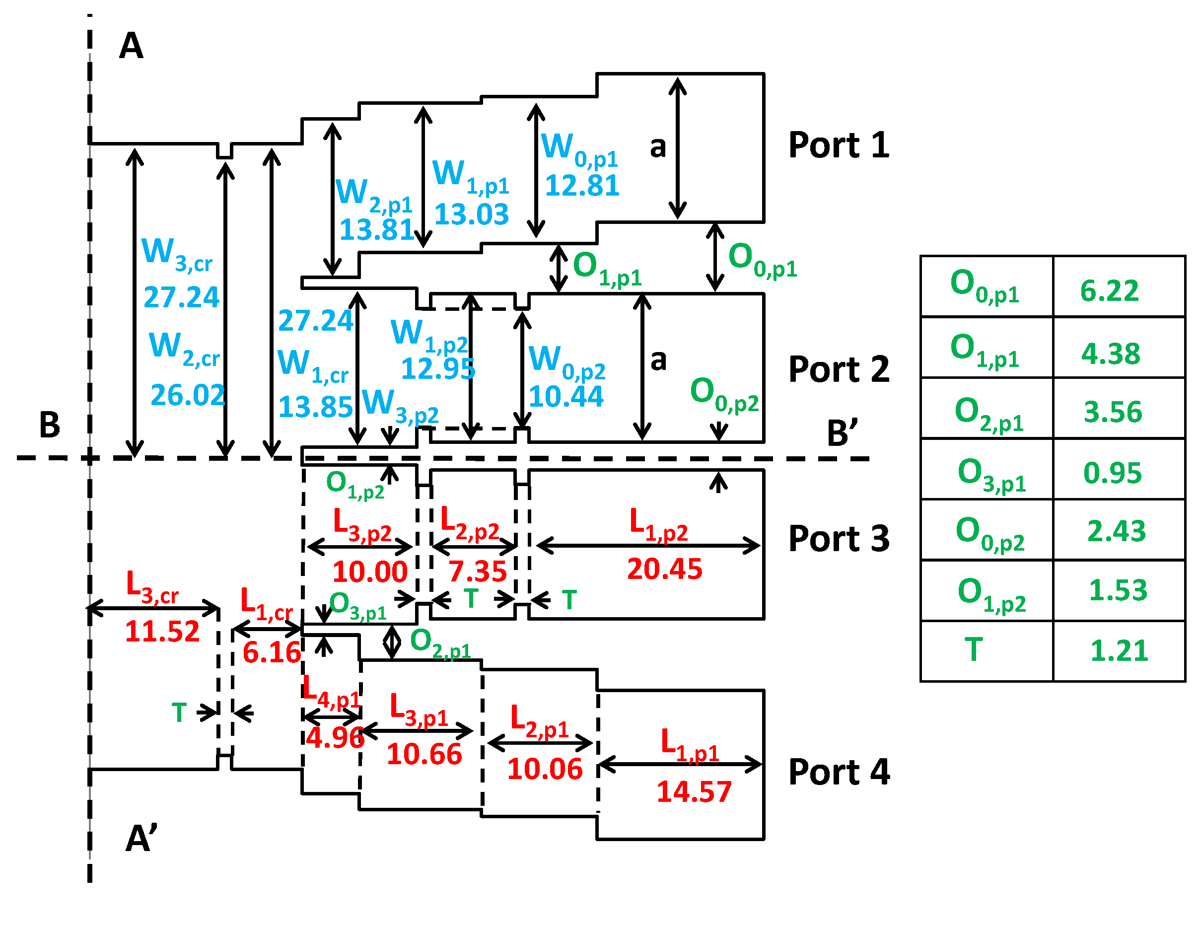
2. Theory and Design

The proposed coupler is presented in Figure 1. For the analysis and design, the structure was split into several building blocks described as follows. The ports were standard rectangular waveguides (WR-51 for this Ku frequency band) with a = 12.95 mm and b = 6.48 mm. Routing arms with H-plane discontinuities in the waveguide width were used to transfer the signal from the input ports to the central coupling region. These elements were designed to have a coupling with the same transmission to all the output ports. Considering the layout shown in Figure 1a, this meant that the magnitude of S j , 1 and S j , 2 with j = 5 , , 8 , should be close to −6 dB, keeping the isolation S j , 1 , j = 2 , 3 , 4 , and S j , 2 , j = 1 , 3 , 4 , as low as possible. Since the coupler had two-fold symmetry and could be divided into four equal parts, the analysis of the network was simplified, and the other S-parameters were obtained by symmetry. In fact, considering the coupler symmetries in Figure 1b (planes AA’ and BB’), the analysis reduced to two-port structures with appropriate boundary conditions of a perfect electric wall and a perfect magnetic wall at planes AA’ and BB’.
For the design of the coupler, firstly, the structure was divided into two parts: routing arms and the coupling region. Due to the coupler symmetry, Port 1 was equivalent to Ports 4, 5, and 8, while Port 2 was equivalent to Ports 3, 6, and 7. The routing arms of Port 1 were composed of several off-center blocks. The routing arms of Port 2 were composed of several blocks and irises. The initial dimensions of the routing arms of the coupler were based on the six-port coupler of [5]. Secondly, the connection of the N = 8 routing arms coming from the ports of the coupler, as in Figure 1, was performed through a coupling region with an initial width equal to a × N / 2 , where a was the width of the standard WR-51 waveguide of the ports. Hence, the initial width was 51.8 mm, allowing the propagation of the higher order mode T E 40 in this coupling region. Finally, the dimensions for the routing arms and the coupling region were optimized to fulfill the electrical specifications shown in Table 1, where it can be seen that the design central frequency was set to 15.1 GHz (with a bandwidth of 1 GHz).
Once the initial dimensions of the routing arms and the coupling region were defined, a suitable cost function for the coupler structure to be optimized was found to be:
f = i = 1 N f r e q w i 1 | | S 11 g o a l | | S 11 | | 2 + w i 1 | | S 22 g o a l | | S 22 | | 2 + w i 1 | | S 21 g o a l | | S 21 | | 2 + w i 1 | | S 31 g o a l | | S 31 | | 2 + w i 1 | | S 41 g o a l | | S 41 | | 2 + w i 2 | | S 51 g o a l | | S 51 | | 2 + w i 2 | | S 61 g o a l | | S 61 | | 2 + w i 2 | | S 71 g o a l | | S 71 | | 2 + w i 2 | | S 81 g o a l | | S 81 | | 2 + w i 2 | | S 62 g o a l | | S 62 | | 2 + w i 2 | | S 72 g o a l | | S 72 | | 2
where | S i j g o a l | is the theoretical magnitude of the scattering parameter to be achieved (from Table 1), S i j is the scattering parameter obtained by full-wave simulation, and w i N are optimization weights. The weights of the cost function (1) were set to w i 1 = 1, for the return losses ( S 11 , S 22 ) and considered isolations ( S 21 , S 31 , and S 41 ) and w i 2 = 2, for the considered couplings ( S 51 , S 61 , S 71 , S 81 , S 62 , and S 72 ). N f r e q was the number of frequency points taken into account for the optimization, which could range from three points in the first optimization iterations to a number as large as 10 in the last iterations. An in-house software tool based on the MM method was used to obtain the full-wave simulation results. MM was used in a modular way to calculate the generalized scattering matrix of each building block, which were later connected to achieve an overall response of [12,13,14,15].
The achieved structure and dimensions are shown in Figure 2. As can be seen, the lengths ( L i ), widths ( W i ), offsets ( O i ), and irises’ thickness (T) for Routing Arms 1 and 2, as well as for the coupling region, were used as the variables in the optimization process. The dimensions in the figure are in millimeters. Figure 3 shows the simulated return losses, couplings, and isolations of the coupler considered in (1) for Port 1 and Port 2 (the value of the S-parameters for equivalent ports in the coupler was the same because of symmetries). The final length of the coupling region after the optimization was 1.9 λ , and its width was 2.7 λ , where λ was the free space wavelength at 15.1 GHz. The coupler was validated by CST Microwave Studio prior to fabrication with additive manufacturing, showing similar results to MM, as can be seen in Figure 3. Figure 4a,b show the electric field distribution in the directional coupler, when it was fed with the T E 10 mode through Port 1 and Port 2, respectively. As expected, the electric field distribution of the T E 40 mode in the central region of the problem can be seen in the figure.
Table 2 presents the simulated electrical performance of This Work (TW) compared with other configurations of aperture type-couplers, considering relative Bandwidth (BW), return loss, coupling, number of Physical (Phy.) and Electrical (Elec.) ports, and size. For the case of eight physical ports with one mode per port, this work provides a very simple H-plane structure with enough bandwidth for networks with eight ports.

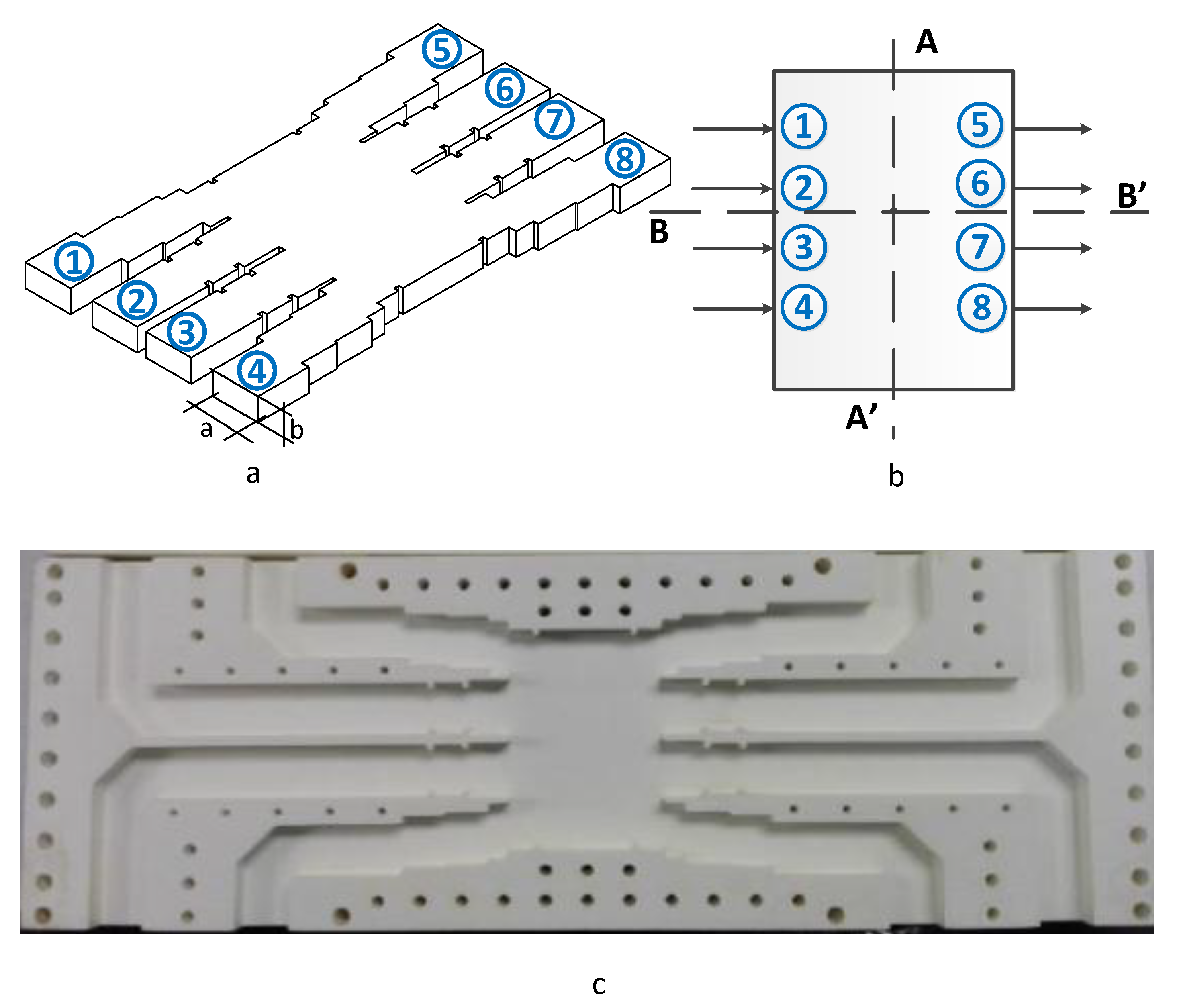
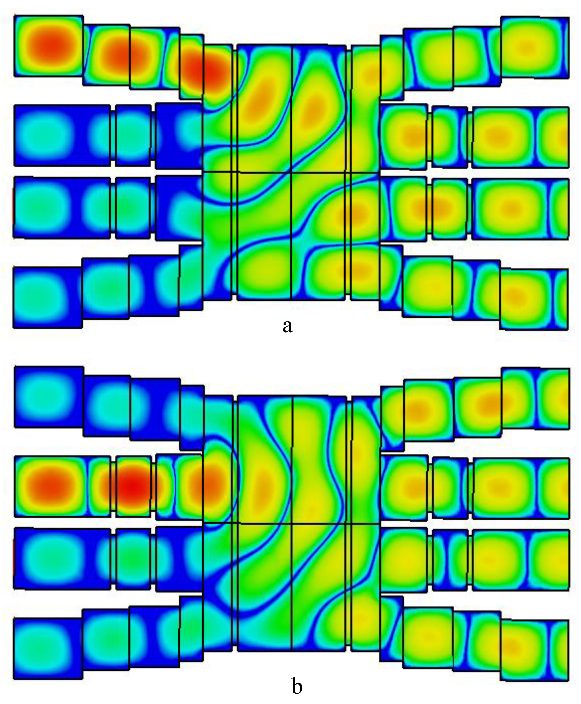
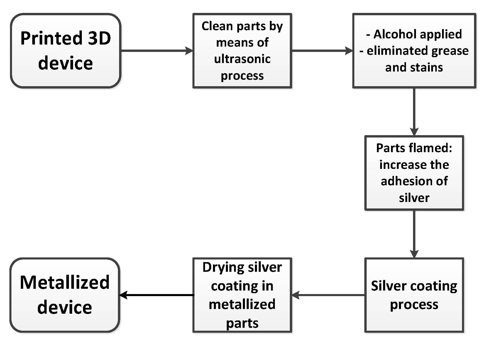
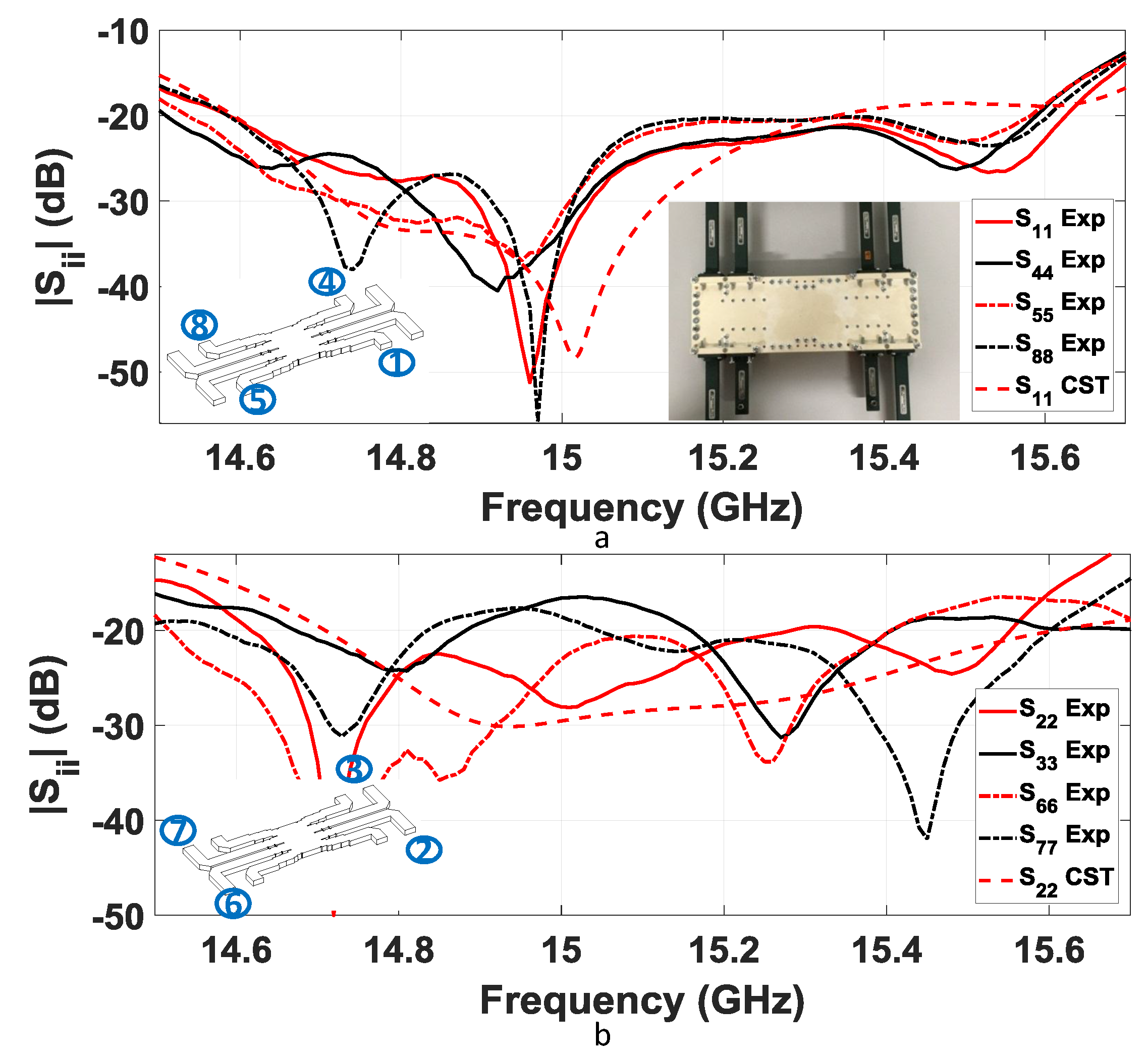
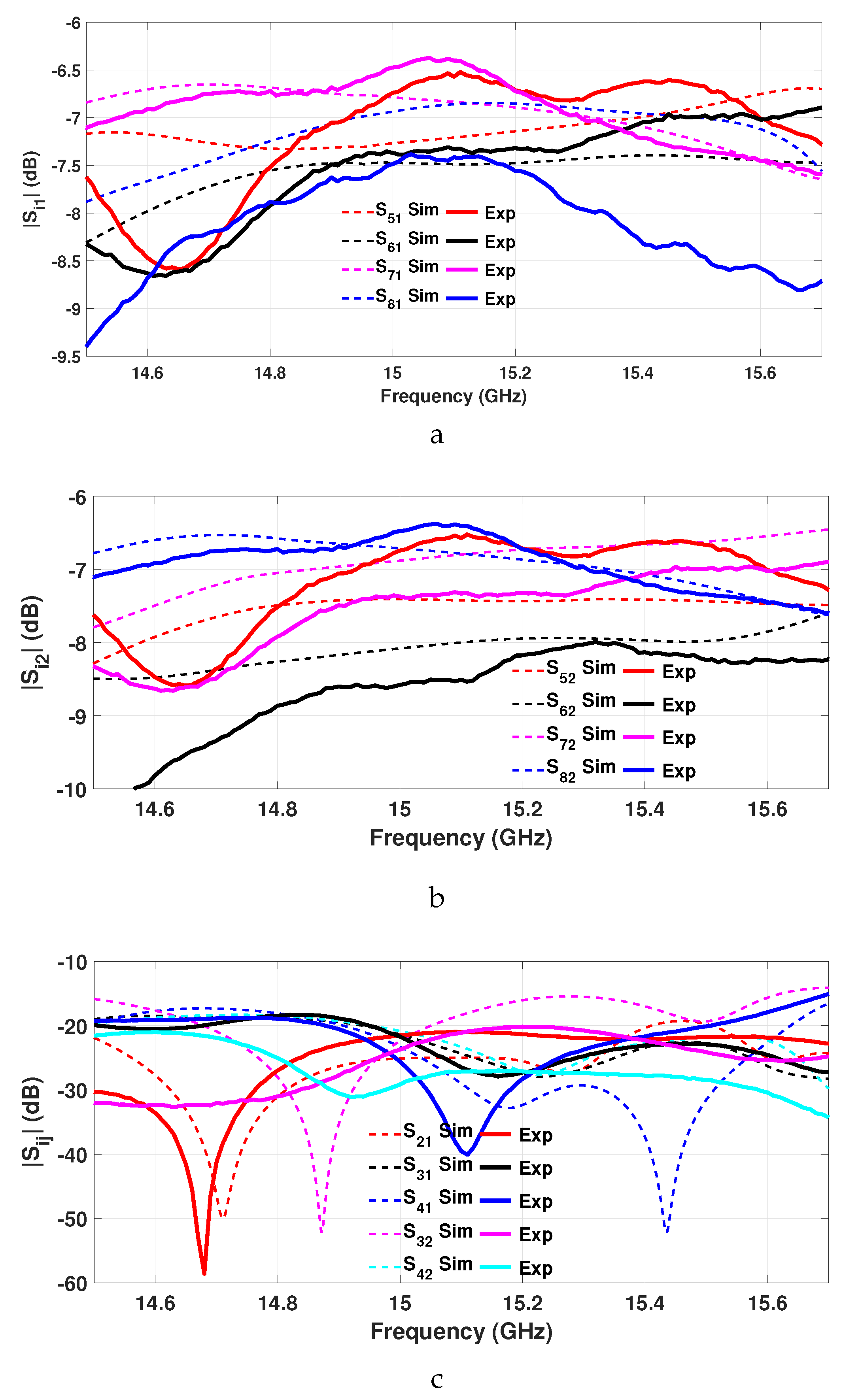
3. Experimental Prototype with Additive Manufacturing and Results

Additive manufacturing [16,17] using plastic was used for the prototype implementation. Since the 3D printed waveguide components were manufactured from plastic, they must be metalized using either copper [16,17] or silver [18]. A 3D printer was used with Polylactic Acid (PLA biopolymer) material. Given the fact that the ports were very close to each other, waveguide bends were added to the ports to perform measurements. All fabricated parts were metalized by silver coating. The layer of the silver coating had a thickness of 2.0 μ m. Before metallization, all parts were cleaned using an ultrasonic cleaning process to remove all dust and particles on the surface; then, isopropyl alcohol was applied to eliminate grease and stains. The parts were flamed to increase the surface tension of the substrate and the adhesion of silver coating. Subsequently, an activation solution was sprayed on the surface to accelerate the initiation of the chemical reaction. Next, metallization solutions were sprayed to create a silver coating on the whole surface. Finally, all parts were dried by air pressure to evacuate the water film. Figure 1c shows the main printed part of the coupler prototype, fabricated and metalized by silver coating. In this work, the fabrication of a prototype with a low cost and low printing time was the aim. The procedure used in this work is shown in Figure 5.
S-parameter measurements were performed using a Keysight E5071C ENA series network analyzer over the frequency range from 14.5 to 15.7 GHz. Figure 6a,b show the return loss for Ports 1, 4, 5, and 8 and for Ports 2, 3, 6, and 7, respectively. The obtained return losses for each port were very similar, although the manufacturing tolerances led to a deviation in the measured response, especially in Ports 3 and 7.
Figure 7a,b show the experimental results for the S-parameters associated with the coupling. The dashed lines show the full-wave simulation response, and the solid lines show the experimental response. The simulation results of the coupler took a bad contact between the lid and the structure into account. This bad contact appeared in the manufactured device when there was no option to put enough screws to tighten the main part with the lid, as happened in the coupling region of the present design. The bad contact was modeled with a separation between the lid and the structure of 0.02 mm.
In order to see this effect, Figure 8 shows the simulations (results obtained with CST) of the coupling between Ports 5 and 1 ( S 51 parameter), when the gap between the lid and the main body was modified in steps of 0.01 mm. This type of effect was observed in other H-plane structures built with the same approach of a body plus lid [19,20].
Each additional separation of 0.01 mm translated into approximately a 0.2 dB increase in losses. The effective conductivity (nominal conductivity of the metallization including the surface roughness) considered in the simulation in Figure 7 was 2.3 MS /m. Isolation of the coupler is shown in Figure 7c, for Port 1 and Port 2. The results from the simulation and measurements showed a similar behavior, validating this low cost additive manufacturing approach for prototyping.

4. Conclusions

A compact H-plane short-slot rectangular waveguide coupler with equal power division, with four-input and four-output ports at the Ku-band, was designed and fabricated by additive manufacturing technology in PLA with silver coating. A theoretical bandwidth of 6.6 % was achieved with a return loss level of 20 dB. The simulated performance of coupling, isolation, and matching was validated with an experimental prototype, where the tolerances of the low cost prototype manufacturing were taken into account. The results showed the potential of the introduced structure for systems requiring distribution networks with a high number of ports.

Author Contributions

Conceptualization and methodology, R.V.H.-B. and J.A.R.-C.; software and validation, R.V.H.-B., J.A.R.-C. and J.C.; writing–original draft preparation, writing–review and editing, R.V.H.-B., J.A.R.-C. and J.C.; supervision, J.A.R.-C, J.R.M.-G. and J.M.R. All authors have read and agreed to the published version of the manuscript.

Funding

This work was supported by the Spanish Government (Agencia Estatal de Investigación, Fondo Europeo de Desarrollo Regional: AEI/FEDER, UE) under Grants TEC2016-76070-C3-1/2-R.

Acknowledgments

The authors would like to thank Jet Metal for the Vacuum Metallization Process used in the construction of the prototype.

Conflicts of Interest

The authors declare no conflict of interest.

References

  1. Uher, J.; Bornerman, J.; Rosenberg, U. Waveguide Components for Antenna Feed Systems: Theory and CAD; Artech House: Boston, MA, USA, 1993. [Google Scholar]
  2. Riblet, H.J. The Short-Slot Hybrid Junction. Proc. IRE 1948, 40, 180–184. [Google Scholar] [CrossRef]
  3. Alessandri, F.; Ravanelli, R. A New Class of Dual-Mode Directional Couplers for Compact Dual-Polarization Beam-Forming Networks. IEEE Microw. Guid. Wave Lett. 1997, 7, 300–301. [Google Scholar] [CrossRef]
  4. Ruiz-Cruz, J.A.; Montejo-Garai, J.R.; Rebollar, J.M. Short-slot E- and H-plane waveguide couplers with an arbitrary power division ratio. Int. J. Electron. 2011, 98, 11–24. [Google Scholar] [CrossRef]
  5. Alessandri, F.; Giordano, M.; Guglielmi, M.; Martirano, G.; Vitulli, F. A New Multiple-Tuned Six-Port Riblet- Type Directional Coupler in Rectangular Waveguide. IEEE Trans. Microw. Theory Tech. 2003, 51, 1441–1448. [Google Scholar] [CrossRef]
  6. Fonseca, N.J.G.; Petrolati, D.; Angeletti, P. Design of a Waveguide Dual-Mode Three-Way Power Divider for Dual-Polarization Beam Forming Networks at Ka-Band. In Proceedings of the 2013 IEEE Antennas and Propagation Society International Symposium (APSURSI), Orlando, FL, USA, 7–13 July 2013; pp. 1096–1097. [Google Scholar]
  7. Morini, A.; Baldelli, M.; Angeletti, P.; Petrolati, D.; Toso, G.; Venanzoni, G. Directional Coupler with 3 Input / 3 Output Square Waveguide Dual-Polarization Ports. In Proceedings of the 12th European Conference on Antennas and Propagation (EuCAP 2018), London, UK, 9–13 April 2018; pp. 1–4. [Google Scholar]
  8. Kim, D.H.; Hirokawa, J.; Ando, M. Design of Waveguide Short-Slot Two-Plane Couplers for One-Body 2-D Beam-Switching Butler Matrix Application. IEEE Trans. Microw. Theory Tech. 2016, 64, 776–784. [Google Scholar] [CrossRef]
  9. Hirokawa, J.; Kim, D.; Wakasa, M.; Sunaguchi, Y.; Tomura, T.; Nishimori, K. Measurements of a 64x64-way One-body Two-dimensional Beam-switching Hollow-waveguide Butler Matrix. In Proceedings of the 2018 48th European Microwave Conference EuMW, Madrid, Spain, 23–27 September 2018; pp. 125–128. [Google Scholar]
  10. Ahmadi, S. 5G Arquitecture, Technology, Implementation, and Operation of 3GPP New Radio Standards; Elsevier: London, UK, 2019; pp. 566–586. [Google Scholar]
  11. Razavizadeh, S.M.; Ahn, M.; Lee, I. Three-Dimensional Beamforming. IEEE Signal Process. Mag. 2014, 94, 94–101. [Google Scholar] [CrossRef]
  12. Conciauro, C.; Guglielmi, M.; Sorrentino, R. Advanced Modal Analysis: CAD Techniques for Waveguide Components and Filters; John Wiley: Hoboken, NJ, USA, 1999. [Google Scholar]
  13. Alessandri, F.; Bartolucci, G.; Sorrentino, R. Admittance matrix formulation of waveguide discontinuity problems: Computer aided design. IEEE Trans. Microw. Theory Tech. 1988, 36, 394–403. [Google Scholar] [CrossRef]
  14. Rebollar, J.M.; Esteban, J.; Page, J.E. Fullwave analysis of three and four-port rectangular waveguide juctions. IEEE Trans. Microw. Theory Tech. 1994, 42, 256–273. [Google Scholar] [CrossRef]
  15. Ruiz-Cruz, J.A.; Montejo-Garai, J.R.; Rebollar, J.M. Computer Aided Design of Waveguide Devices by Mode-Matching Methods; Intechopen: London, UK, 2010; pp. 1–26. [Google Scholar] [CrossRef] [Green Version]
  16. Moscato, S.; Bahr, R.; Le, T.; Pasian, M.; Bozzi, M.; Perregrini, L.; Tentzeris, M.M. Additive manufacturing of 3D substrate integrated waveguide components. Electron. Lett. 2015, 51, 1426–1428. [Google Scholar] [CrossRef]
  17. Tamayo-Dominguez, A.; Fernández, J.M.; Sierra-Perez, M. Groove Gap Waveguide in 3-D Printed Technology for Low Loss, Weight, and Cost Distribution Networks. IEEE Trans. Microw. Theory Tech. 2017, 65, 4138–4147. [Google Scholar] [CrossRef]
  18. Shen, J.; Aiken, M.; Ladd, C.; Dickey, M.D.; Ricketts, D.S. A simple electroless plating solution for 3D printed microwave components. In Proceedings of the 2016 Asia-Pacific Microwave Conference, New Delhi, India, 5–9 December 2016. [Google Scholar]
  19. Montejo-Garai, J.R.; Ruiz-Cruz, J.A.; Rebollar, J.M. Full-Wave Design of H-Plane Contiguous Manifold Output Multiplexers Using the Fictitious Reactive Load Concept. IEEE Trans. Microw. Theory Tech. 2005, 53, 2628–2632. [Google Scholar] [CrossRef]
  20. Montejo-Garai, J.R.; Ruiz-Cruz, J.A.; Rebollar, J.M. Efficient Design of Contiguous-Band Elliptic-Response Manifold Output Multiplexers with Single-Terminated Filters. Electromagnetics 2010, 30, 644–659. [Google Scholar] [CrossRef]
Figure 1. (a) Layout of the eight-port coupler. (b) Block diagram of the eight-port coupler with two symmetry axes. (c) Fabricated part by additive manufacturing.
Electronics 09 00610 g001
Figure 2. Optimized dimensions in the coupler (mm): Length (L ), Width (W), Offset (O), and Thickness (T) of the ports and the coupling region (showing one half of the structure).
Electronics 09 00610 g002
Figure 3. Simulated results of return losses, couplings, and isolations by Mode-Matching (MM) (solid lines) and CST (dashed lines) considered in (1) for Port 1 and Port 2.
Electronics 09 00610 g003
Figure 4. E-field distribution of the coupler when it is fed by: (a) Port 1 and (b) Port 2.
Electronics 09 00610 g004
Figure 5. Flowchart for the metallization process of the directional coupler.
Electronics 09 00610 g005
Figure 6. Experimental results for the return loss for the eight ports. (a) Ports 1, 4, 5, and 8. (b) Ports 2, 3, 6, and 7. The numbering of the ports is shown in the inset of the figure. Simulation results are presented with dashed lines.
Electronics 09 00610 g006
Figure 7. Simulated (Sim) results (taking the conductivity and space between the structure and the lid of the prototype into account) and experimentally (Exp) measured parameters for: (a) Coupling Port 1; (b) Coupling Port 2. (c) Isolation performance for Port 1 and Port 2.
Electronics 09 00610 g007
Figure 8. Simulation results of coupling S 5 , 1 varying the gap between the lid and the main body in steps of 0.01 mm.
Electronics 09 00610 g008
Table 1. General electrical specifications of the eight-port coupler.
SpecificationsRequirements
Number of Ports8
Central Frequency15.1 GHz Ku band
Bandwidth1 GHz 6.6 %
Return Loss< 20 dB
Isolation< 20 dB
Coupling Values6.02 ± 1 dB
InterfaceWaveguide WR-51
Table 2. Comparison of different types of aperture-type couplers having diverse physical and electrical ports. BW, Bandwidth; Phy, Physical; Elec., Electric; TW, This Work.
Ref.BW (%)Return Loss (dB)Coupling. (dB)No. of Phy./Elec. PortsSize
[4]15.025.0−3.01 ± 0.54/4Low
 [3]8.325.0−3.01 ± 0.54/8Low
 [5]8.420.0−4.77 ± 1.06/6High
 [6]10.020.0−4.77 ± 1.06/12Medium
 [8]2.318.5−6.02 ± 1.08/8Medium
TW6.620.0−6.02 ± 1.08/8Medium

