Abstract
This paper presents a scaled GaN-HEMT large-signal model based on EM simulation. A large-signal model of the 10-finger GaN-HEMT consists of a large-signal model of the two-finger GaN-HEMT and an equivalent circuit of the interconnection circuit. The equivalent circuit of the interconnection circuit was extracted according to the EM simulation results. The large-signal model for the two-finger device is based on the conventional Angelov channel current model. The large-signal model for the 10-finger device was verified through load-pull measurement. The 10-finger GaN-HEMT produced an output power of about 20 W for both simulation and load-pull measurements.
1. Introduction
Recently, as a result of high-power density, high breakdown voltage, and high-frequency characteristics, the gallium nitride high electron mobility transistor (GaN-HEMT) has been widely utilized for RF power amplifiers for various applications including base stations for wireless communication systems, satellite communication systems, and radars. In addition to the hybrid RF power amplifiers, monolithic microwave integrated circuits (MMICs) using GaN-HEMT have also been developed [1,2,3,4,5]. An accurate large-signal transistor model is essential in designing circuits with high performances and also in reducing the design time. Additionally, accurate measurement of the device is crucial for accurate model extraction.
In regards to precise large-signal modeling, large-signal electro-thermal or empirical models of GaN-HEMT and silicon laterally-diffused metal-oxide-semiconductor field-effect transistors (LDMOS-FET) have been studied [6,7,8,9,10,11]. In [6], a compact channel current model was constructed with a reduced number of parameters. Electro-thermal large-signal models were proposed in [8,9,10,11]. In [12], a channel current considering the device physics was proposed. Most of the previous transistor models with various output power capacities are directly based on the measured results for the transistor itself [12,13,14,15,16]. However, in the case of transistors with a high output power capacity, it is very difficult to obtain an accurate large-signal model directly. This is a result of increased measurement error in both the DC I-V characteristics owing to the increased thermal effect and the small-signal characteristics due to very low input and output impedances. Therefore, it is desirable to extract an accurate large-signal model using a small-sized transistor and then scale the model for the larger-sized transistor.
In this paper, a large-signal modeling technique for a high-power GaN-HEMT is proposed using a large-signal model of a relatively smaller device and an electro-magnetic (EM) simulation for the interconnection circuit. As a unit device, a two-finger GaN-HEMT is selected and modeled using the measured I-V and small-signal characteristics. Later, a large-signal model of the 10-finger device, consisting of five unit devices and an interconnection circuit, is developed using the large-signal model of the unit device and an equivalent circuit for the interconnection circuit. Generation and simulation of the interconnection circuit is done using a 2.5D EM simulation tool in order to extract its equivalent circuit. The large-signal model of the 10-finger device is verified by comparing the results from the harmonic balance simulation and the load-pull measurement.
2. Large-Signal Model of The Unit Device
Figure 1 shows the layout of the two-finger GaN-HMET in (a) and its equivalent circuit in (b). The equivalent circuit consists of non-linear components (, , and ), linear parasitic components (, , , , , and ), and the nonlinear current source () [17,18]. Furthermore, in order to model the substrate effect, a series R-C network ( and ) is added [19]. Extraction of the parameters must be accurate in a wide frequency and operational range in both the voltage and current.
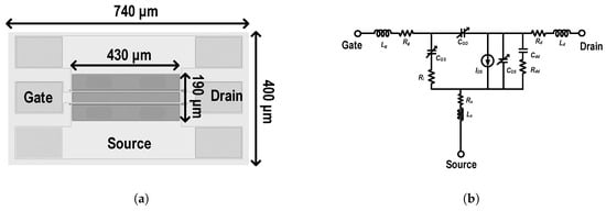
Figure 1.
Two-finger GaN-HEMT: (a) layout; (b) equivalent circuit.
2.1. Channel Current Model
The Angelov current model was used to model the channel current of the unit GaN-HEMT empirically [9,10,11,12]. The model has been widely applied and verified. It can be described as follows:
where represents the drain current where the maximum transconductance occurs. is a parameter to represent the channel length modulation. is a parameter to represent the saturation voltage. is presented as follows.
where , , and are fitting coefficients. represents the threshold voltage. and are given as follows.
where , , B, , and are fitting coefficients.
The measured pulsed I-V(PIV) data with a pulse width of 1 µs and a duty cycle of 10% was modeled using the channel current model. The model parameters were extracted using Keysight’s Advanced Design System (ADS). The extracted parameter values for the channel current are presented as in Table 1.

Table 1.
Extracted parameter values for the channel current of the unit GaN-HEMT.
Figure 2 shows the measured and modeled PIV of the unit two-finger GaN-HEMT. The gate voltage (Vgs) range of the measured and modeled PIV data was from −2.5 V to 0 V, while the drain voltage (Vds) range was from 0 to 60 V. According to the extracted parameters in Table 1, the modeled and measured PIV were consistent.
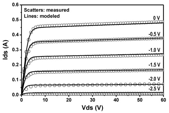
Figure 2.
Measured and modeled pulsed-IV (PIV) results.
2.2. Modeling the Non-Linear Capacitors
Linear parasitic components were extracted prior to the extraction of the nonlinear components. A multi-point simultaneous optimization technique was adopted [6]. The non-linear components of the GaN-HEMT should be accurately modeled for a wide operating range in terms of both current and voltage. Non-linear components of the unit GaN-HEMT included the gate-source capacitor (), gate-drain capacitor (), and drain-source capacitor () [9,12,20]. Each component was extracted based on the measured S-parameter of a wide operation range, and based on the extracted data, the nonlinear capacitors were empirically modeled using continuous and differentiable functions [9,10,11,12,13,14,15]. The modeled non-linear components are expressed as follows:
where to , to , and to are constants optimized to fit the extracted nonlinear components.
Figure 3 presents the extracted versus modeled non-linear components. While the varied dominantly based on the gate voltage, the and varied dominantly based on the drain voltages. All the modeled non-linear components were consistent with the extracted component values over a wide operating range. The extracted parameters for the nonlinear capacitors are presented in Table 2.
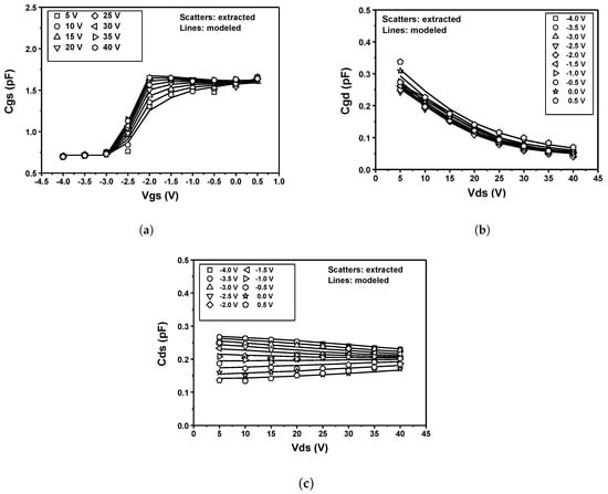
Figure 3.
Extracted and modeled non-linear capacitors over the wide operating range: (a) , (b) , (c) .
Table 2.
Model parameters for the nonlinear components.
2.3. Model Verification of the Two-Finger GaN-HEMT
The unit GaN-HEMT large-signal model was verified using the measured S-parameters and the load-pull measurements. Figure 4 presents the measured and modeled S-parameters in the frequency range from 0.1 to 10 GHz for gate bias voltage (Vgs) of −2.0 V and drain bias voltage (VDD) of 30 V for the large-signal of the unit GaN-HEMT. This was a Class-AB condition with a quiescent current of 15 mA. The measured and modeled results were consistent with each other. Figure 5 presents the load-pull measurement and simulation results at a frequency of 3.5 GHz using the two-finger GaN-HEMT large-signal model. The simulated GaN-HEMT produced a gain of 12.1 dB, a peak output power of 36.3 dBm, and a maximum efficiency of 57.7%. The load-pull measurement showed nearly similar results with a gain of 12.2 dB, a peak output power of 36.0 dBm, and a power added efficiency (PAE) of 55.4%.
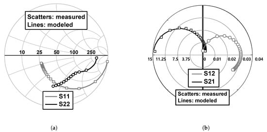
Figure 4.
Measured and modeled S-parameters of the two-finger GaN-HEMT for Vgs of −2.0 V and VDDof 30 V in the frequency range from 0.1 to 10 GHz: (a) S11 and S22; (b) S12 and S21.
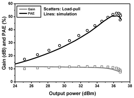
Figure 5.
Load-pull measurement and simulation results of the unit GaN-HEMT at a frequency of 3.5 GHz.
3. Scaled Model for The 10-Finger GaN-HEMT
The model of the 10-finger GaN-HEMT was extended according to the large-signal model of the two-finger GaN-HEMT, which was accurately modeled with the measured data. Extra pads and interconnection circuits were modeled using the equivalent circuit, which was based on EM simulation. Figure 6 shows the layout of the 10-finger GaN-HEMT, which consisted of five two-finger devices. The two-finger devices were combined using gate and drain pads.
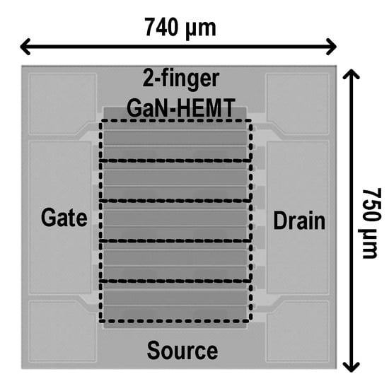
Figure 6.
Layout of the 10-finger GaN-HEMT.
Figure 7a shows the layout of the gate or drain pad of the 10-finger GaN-HEMT for the EM simulation. Figure 7b shows its equivalent circuit. Five units of two-finger GaN-HEMTs were combined into one pad. The equivalent circuit consisted of shunt capacitors and a multiple series inductor and resistor for the pad. Keysight’s ADS Momentum, a 2.5D EM simulation tool, was used to simulate the layout of the pad.
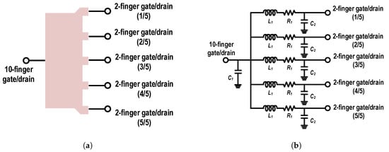
Figure 7.
(a) Layout of the gate or drain pad; (b) equivalent circuit of the gate or drain pad.
Figure 8 presents the comparison between the EM simulation results and the circuit simulation results of the equivalent circuit. The results of the EM and circuit simulation were matched with each other through a wide frequency range from 0.1 to 10 GHz. The extracted component values of the equivalent circuit were as follows: of 53.8 fF, of 11.1 fF, of 18.6 pH, and of 3 mΩ. Figure 9 presents the overall equivalent circuit of the 10-finger GaN-HEMT using a combination of five-unit devices and equivalent circuits of the pads.
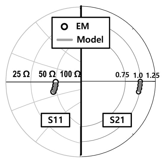
Figure 8.
EM simulation results for the layout versus circuit simulation results for the equivalent circuit of the pad.
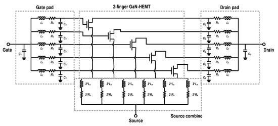
Figure 9.
Overall equivalent circuit of the 10-finger GaN HEMT.
Figure 10 presents the simulated PIV characteristics using the scaled large-signal model of the10-finger GaN-HEMT. Figure 11 shows the load-pull simulation and measurement results for the 10-finger GaN-HEMT using a continuous wave (CW) signal at a frequency of 3.5 GHz and a quiescent current of 100 mA. The measured and simulated power gains were almost similar with values of 13.7 and 13.5 dB, respectively. The measured and simulated PAEs were also almost similar with values of 54.2 and 57.2%, respectively. The output power attained about 20 W for the measured results which was almost five-times larger compared to that of the unit two-finger device (about 4 W).
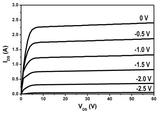
Figure 10.
Simulated PIV for the modeled 10-finger GaN-HEMT.
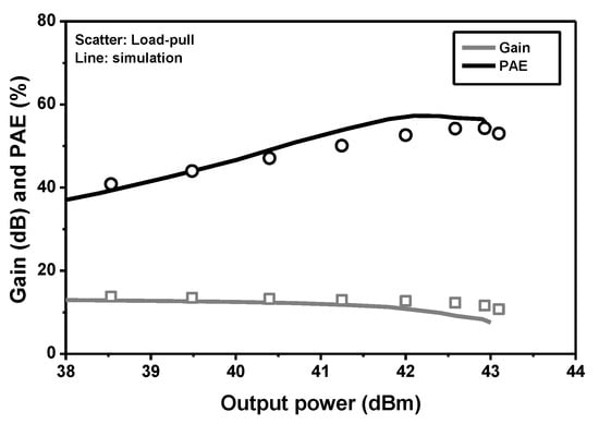
Figure 11.
Simulated and measured gain and PAE of the scaled 10-finger GaN-HEMT at a frequency of 3.5 GHz.
4. Conclusions
In this paper, a scaled empirical large-signal model of the multi-finger GaN-HEMT using the conventionally modeled large-signal model of the unit device and the equivalent circuits of the interconnection circuits and pads was presented. The equivalent circuits of the interconnection circuits and pads were extracted from the EM simulation for its layout. Regarding verification, the 10-finger GaN-HEMT was modeled according to the large-signal model of the unit two-finger device and the equivalent circuits of the pads.
For the large-signal model of the two-finger GaN-HEMT, the Angelov channel current model was adopted for the measured PIV data. The multi-point optimization method was used to obtain the linear components. Empirical functions were used to model the non-linear components using a broad operation range for the voltage and current at the broad frequency range from 0.1 to 10 GHz. The layout of the pad was simulated through a 2.5D EM tool in order to extract its equivalent circuit.
The scaled large-signal model of the 10-finger GaN-HEMT was developed using the five-unit two-finger GaN-HEMTs and the equivalent circuits for the gate and drain pads. The scaled model for the 10-finger GaN-HEMT was proven through conformation of the load-pull measurement to the simulation results. The proposed scaled model could be applied to high-power GaN-HEMTs, which can be used to design high-power RF amplifiers for base-transceiver systems more accurately.
Author Contributions
Conceptualization, W.L. and Y.Y.; methodology, H.K. (Hyunuk Kang), S.C. and S.L.; software, W.L. and H.K. (Hyunuk Kang); validation, W.L., S.C., and H.K. (Hosang Kwon); formal analysis, K.c.H. and K.-Y.L.; investigation, W.L., H.K. (Hyunuk Kang), S.C., and S.L.; resources, W.L.; data curation, W.L. and Y.Y.; writing, original draft preparation, W.L.; writing, review and editing, W.L. and Y.Y.; visualization, Y.Y.; supervision, Y.Y.; project administration, Y.Y.; funding acquisition, Y.Y. All authors read and agreed to the published version of the manuscript.
Funding
The research reported in this work has been supported by ADD (Agency of Defense Development) of Korea under an R&D program (UC170025FD).
Conflicts of Interest
The authors declare no conflict of interest.
References
- Kang, H.; Lee, H.; Lee, W.; Oh, H.; Lim, W.; Koo, H.; Park, C.; Hwang, K.; Lee, K.; Yang, Y. Octave Bandwidth Doherty Power Amplifier Using Multiple Resonance Circuit for the Peaking Amplifier. IEEE Trans. Circuits Syst. I Reg. Pap. 2019, 66, 583–593. [Google Scholar] [CrossRef]
- Lee, H.; Lim, W.; Bae, J.; Lee, W.; Kang, H.; Hwang, K.; Lee, K.; Park, C.; Yang, Y. Highly efficient fully integrated GaN-HEMT Doherty power amplifier based on compact load network. IEEE Trans. Microw. Theory Technol. 2017, 65, 5203–5211. [Google Scholar] [CrossRef]
- Lee, W.; Kang, H.; Lee, H.; Lim, W.; Bae, J.; Koo, H.; Yoon, J.; Hwang, K.; Lee, K.; Yang, Y. Broadband InGaP/GaAs HBT Power Amplifier Integrated Circuit Using Cascode Structure and Optimized Shunt Inductor. IEEE Trans. Microw. Theory Technol. 2019, 65, 5090–5100. [Google Scholar] [CrossRef]
- Jin, C.; Gao, Y.; Chen, W.; Huang, J.; Wang, Z.; Mo, J.; Yu, F. X-Band High-Efficiency Continuous Class B Power Amplifier GaN MMIC Assisted by Input Second-Harmonic Tuning. Electronics 2019, 8, 1312. [Google Scholar] [CrossRef]
- Chen, R.; Li, R.; Zhou, S.; Chen, S.; Huang, J.; Wang, Z. An X-Band 40 W Power Amplifier GaN MMIC Design by Using Equivalent Output Impedance Model. Electronics 2019, 8, 99. [Google Scholar] [CrossRef]
- Yang, Y.; Woo, Y.; Yi, J.; Kim, B. A New Empirical Large-Signal Model of Si LDMOSFETs for High-Power Amplifier Design. IEEE Trans. Microw. Theory Technol. 2001, 49, 1626–1633. [Google Scholar] [CrossRef]
- Santarelli, A.; Giacomo, V. Empirical Modeling of GaN FETs for Nonlinear Microwave Circuit Applications. In Proceedings of the IEEE/MTT-S International Microwave Symposium (IMS), Anaheim, CA, USA, 23–28 May 2010; pp. 1–4. [Google Scholar]
- Torregrosa, G.; Grajal, J.; Peroni, M.; Serino, A.; Nanni, A.; Cetronio, A. Large-Signal Modeling of Power GaN HEMTs Including Thermal Effects. In Proceedings of the 2nd European Microwave Integrated Circuits Conference, Munich, Germany, 9–12 October 2007; pp. 1–4. [Google Scholar]
- Wang, C.; Xu, Y.; Yu, X.; Ren, C.; Wang, Z.; Lu, H.; Chen, T.; Zhang, B.; Xu, R. An Electrothermal Model for Empirical Large-Signal Modeling of AlGaN/GaN HEMTs Including Self-Heating and Ambient Temperature Effects. IEEE Trans. Microw. Theory Technol. 2014, 62, 2878–2887. [Google Scholar] [CrossRef]
- King, J.B.; Brazil, T.J. Nonlinear Electrothermal GaN HEMT Model Applied to High-Efficiency Power Amplifier Design. IEEE Trans. Microw. Theory Technol. 2013, 61, 444–454. [Google Scholar] [CrossRef]
- Yuk, K.; Branner, G.; McQuate, D. A Wideband Multiharmonic Empirical Large-Signal Model for High-Power GaN HEMTs With Self-Heating and Charge-Trapping Effects. IEEE Trans. Microw. Theory Technol. 2009, 57, 3322–3332. [Google Scholar] [CrossRef]
- Xu, Y.; Wang, C.; Sun, H.; Wen, Z.; Wu, Y.; Xu, R.; Yu, X.; Ren, C.; Wang, Z.; Zhang, B.; et al. A Scalable Large-Signal Multiharmonic Model of AlGaN/GaN HEMTs and Its Application in C-Band High Power Amplifier MMIC. IEEE Trans. Microw. Theory Technol. 2017, 65, 2836–2846. [Google Scholar] [CrossRef]
- Ahsan, S.; Ghosh, S.; Khandelwal, S.; Chauhan, Y. Physics-Based Multi-Bias RF Large-Signal GaN HEMT Modeling and Parameter Extraction Flow. IEEE J. Electron. Dev. Soc. 2017, 5, 310–319. [Google Scholar] [CrossRef]
- Xiong, A.; Charbonniaud, C.; Gatard, E.; Dellier, S. A Scalable and Distributed Electro-thermal Model of AlGaN/GaN HEMT dedicated to Multi-fingers Transistors. In Proceedings of the IEEE Compound Semiconductor Integrated Circuit Symposium (CSICS), Monterey, CA, USA, 3–6 October 2010; pp. 1–4. [Google Scholar]
- Zheng, J.; Ma, X.; Lu, Y.; Zhao, B.; Zhang, H.; Zhang, M.; Hao, Y. A Scalabe Active Compensatory Sub-Circuit for Accurate GaN HEMT Large Signal Models. IEEE Microw. Wirel. Compon. Lett. 2018, 26, 431–433. [Google Scholar] [CrossRef]
- Lee, J.; Lee, S.; Webb, K. Scalable Large-Signal Device Model for High Power-Density AlGaN/GaN HEMTs on SiC. In Proceedings of the IEEE/MTT-S International Microwave Symposium (IMS), Phoenix, AZ, USA, 20–24 May 2001; pp. 1–4. [Google Scholar]
- Jarndal, A.; Kompa, G. A New Small-Signal Modeling Approach Applied to GaN Devices. IEEE Trans. Microw. Theory Technol. 2005, 53, 3440–3448. [Google Scholar] [CrossRef]
- Chen, Z.; Xu, Y.; Zhang, B.; Chen, T.; Gao, T.; Xu, R. A GaN HEMTs Nonlinear Large-Signal Statistical Model and Its Application in S-Band Power Amplifier Design. IEEE Microw. Wirel. Compon. Lett. 2016, 26, 128–130. [Google Scholar] [CrossRef]
- Camacho, C.; Aitchison, C. Modelling Frequency Dependence of Output Impedance of A Microwave MESFET At Low Frequencies. Electron. Lett. 1985, 21, 528–529. [Google Scholar] [CrossRef]
- Jardel, O.; Groote, F.; Reveyrand, T.; Jacquet, J.; Charbonniaud, C.; Teyssier, J.; Floriot, D.; Quere, R. An Electrothermal Model for AlGaN/GaN Power HEMTs Including Trapping Effects to Improve Large-Signal Simulation Results on High VSWR. IEEE Trans. Microw. Theory Technol. 2007, 55, 2660–2669. [Google Scholar] [CrossRef]


© 2020 by the authors. Licensee MDPI, Basel, Switzerland. This article is an open access article distributed under the terms and conditions of the Creative Commons Attribution (CC BY) license (http://creativecommons.org/licenses/by/4.0/).