Equivalent Circuit Based Performance Coupling Analysis Method for Lead Wire Interconnection with Defects


Abstract
:1. Introduction
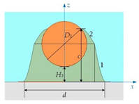
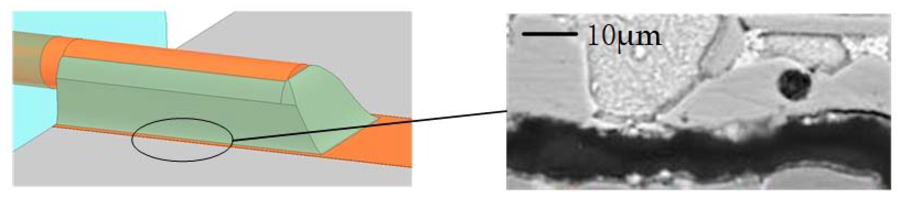
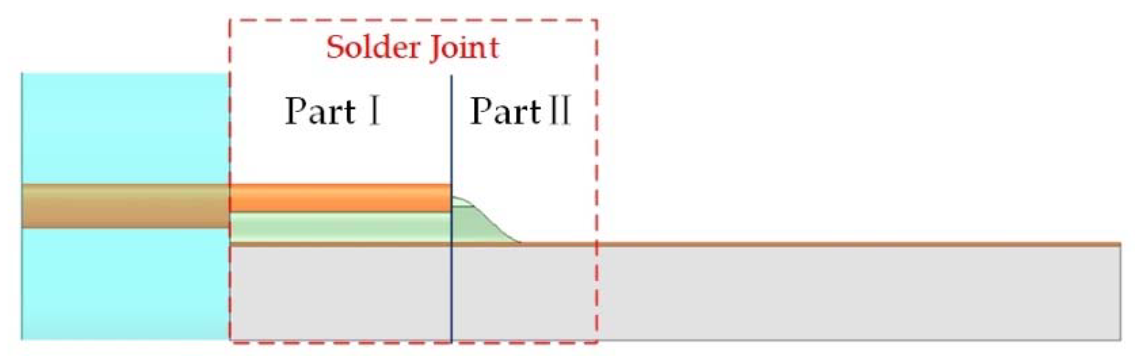
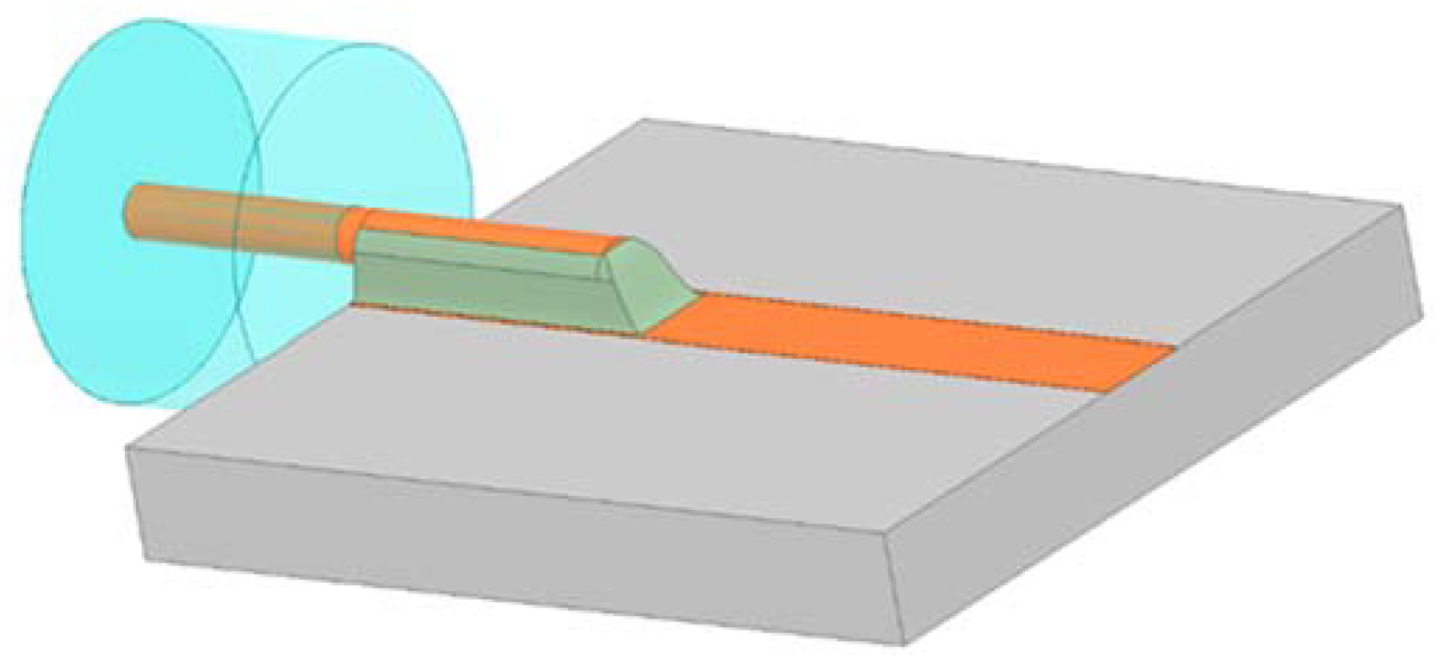
2. Analysis of Structure Characteristics of the Lead Wire Interconnection
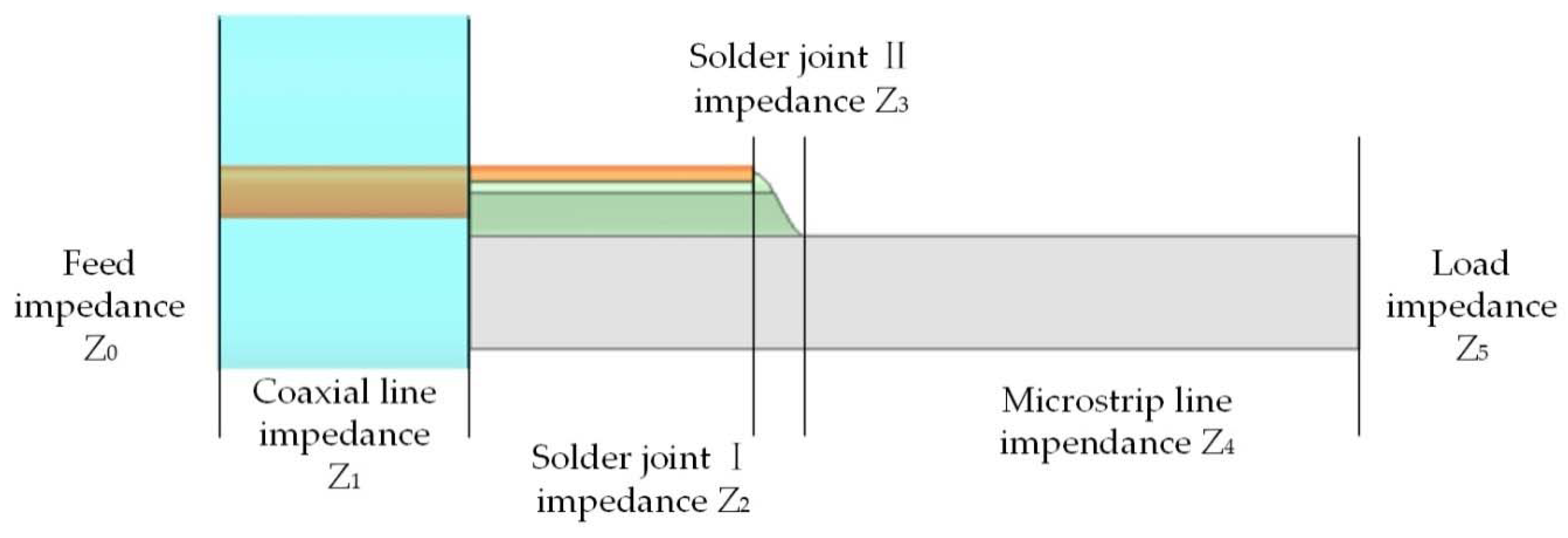
3. Performance Prediction Method of the Solder Joint with the Crack Based on Equivalent Circuit Method
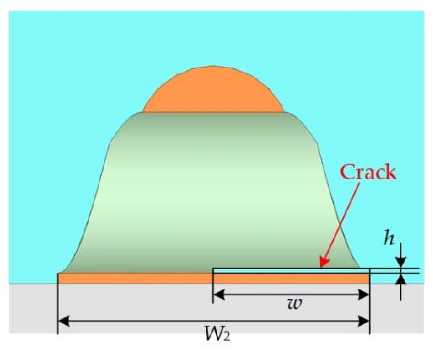
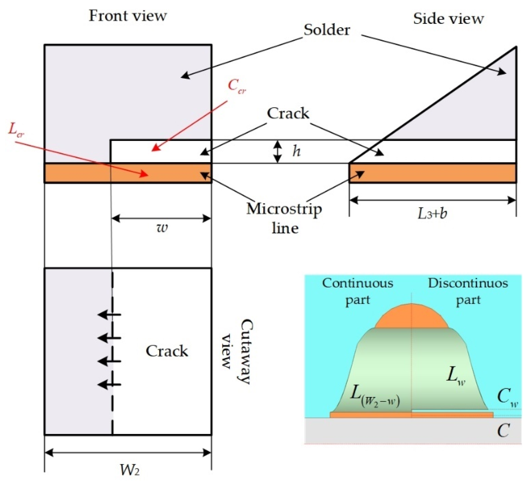
3.1. Extraction of Equivalent Circuit Parameters of the Solder Joint with the Crack
3.2. Calculation Method of Electrical Performance of the Solder Joint with the Crack
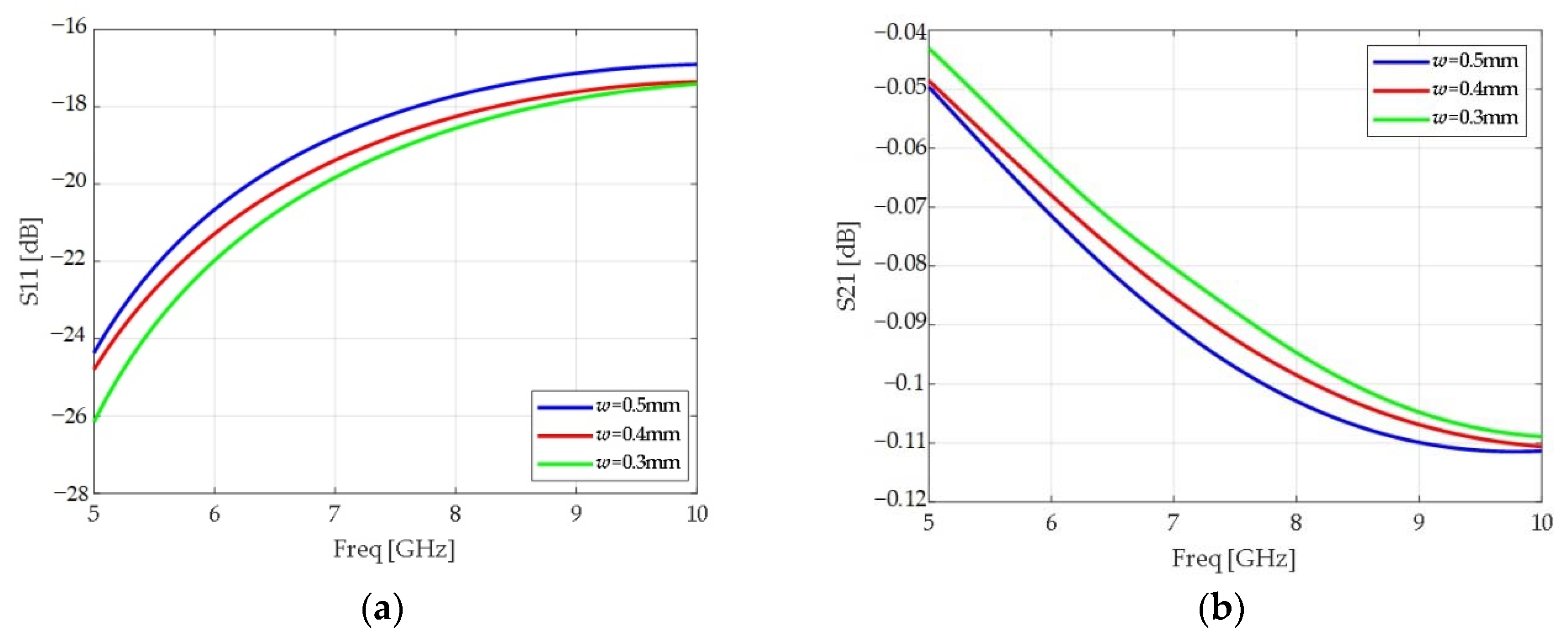
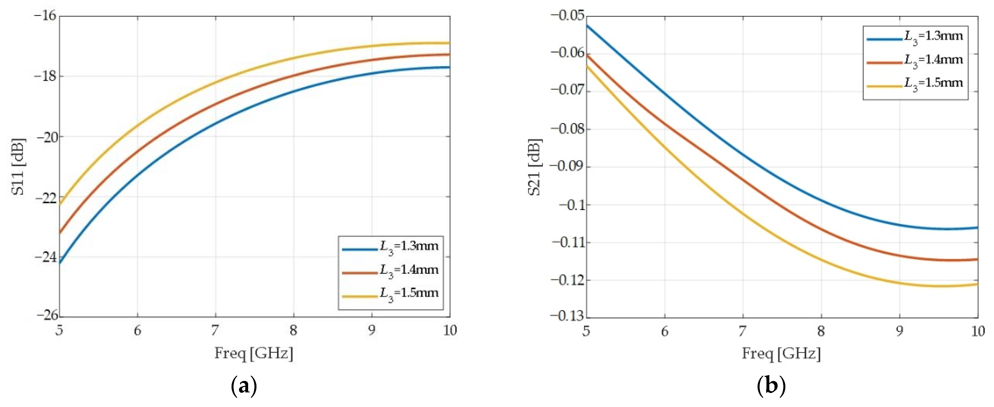
4. Verification and Discussion
5. Conclusions
Author Contributions
Funding
Conflicts of Interest
Appendix A

| Structural Unit | Physical Parameter | Structural Parameter | ||||
|---|---|---|---|---|---|---|
| Material | Relative Permittivity | Loss Tangent | Parameter | Variable | Preset Value (mm) | |
| Dielectric substrate | Al2O3 | 9.9 | 2 × 10⁻⁴ | Length | L1 | 6 |
| Width | W1 | 4.5 | ||||
| Thickness | H1 | 0.635 | ||||
| microstrip line | Au | 1 | 0 | Length | L2 | 6 |
| Width | W2 | 0.6 | ||||
| Thickness | H2 | 0.02 | ||||
| Lead | Diameter | D1 | 0.3 | |||
| Length | L3 | 1.2 | ||||
| Solder joint | Sn37Pb63 | 1 | 0 | End height | a | 0.4 |
| End length | b | 0.3 | ||||
| Side height | c | 0.4 | ||||
| Section width | d | 0.6 | ||||
| Coaxial joint | Insulator | 4 | 1.35 × 10⁻⁵ | Length | L4 | 1.6 |
| Diameter | D2 | 1.8 | ||||
| Crack | Air | 1 | / | Width | w | 0.3 |
| Height | h | 0.01 | ||||

| Solder Joint Shape | Characterization Function | |
|---|---|---|
| Ⅰ | 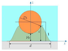 Case 1 | Characterization function 1: |
 Case 2 | Characterization function 1: Characterization function 2: | |
 Case 3 | Characterization function 1: Characterization function 3: | |
| Ⅱ |  End of solder joint |
| Serial Number | L3 | W2 | d | H1 | w | a | c |
|---|---|---|---|---|---|---|---|
| 1 | 0.9 mm | 0.45 mm | 0.45 mm | 0.485 mm | 0 mm | 0.16 mm | 0.16 mm |
| 2 | 0.9 mm | 0.5 mm | 0.5 mm | 0.535 mm | 0.1 mm | 0.21 mm | 0.21 mm |
| 3 | 0.9 mm | 0.55 mm | 0.55 mm | 0.585 mm | 0.2 mm | 0.26 mm | 0.26 mm |
| 4 | 0.9 mm | 0.6 mm | 0.6 mm | 0.635 mm | 0.3 mm | 0.31 mm | 0.31 mm |
| 5 | 0.9 mm | 0.65 mm | 0.65 mm | 0.685 mm | 0.4 mm | 0.36 mm | 0.36 mm |
| 6 | 0.9 mm | 0.7 mm | 0.7 mm | 0.735 mm | 0.5 mm | 0.41 mm | 0.41 mm |
| 7 | 0.9 mm | 0.75 mm | 0.75 mm | 0.785 mm | 0.6 mm | 0.46 mm | 0.46 mm |
| 8 | 1 mm | 0.45 mm | 0.45 mm | 0.535 mm | 0.2 mm | 0.31 mm | 0.36 mm |
| 9 | 1 mm | 0.5 mm | 0.5 mm | 0.585 mm | 0.3 mm | 0.36 mm | 0.41 mm |
| 10 | 1 mm | 0.55 mm | 0.55 mm | 0.635 mm | 0.4 mm | 0.41 mm | 0.46 mm |
| 11 | 1 mm | 0.6 mm | 0.6 mm | 0.685 mm | 0.5 mm | 0.46 mm | 0.16 mm |
| 12 | 1 mm | 0.65 mm | 0.65 mm | 0.735 mm | 0.6 mm | 0.16 mm | 0.21 mm |
| 13 | 1 mm | 0.7 mm | 0.7 mm | 0.785 mm | 0 mm | 0.21 mm | 0.26 mm |
| 14 | 1 mm | 0.75 mm | 0.75 mm | 0.485 mm | 0.1 mm | 0.26 mm | 0.31 mm |
| 15 | 1.1 mm | 0.45 mm | 0.45 mm | 0.585 mm | 0.4 mm | 0.46 mm | 0.21 mm |
| 16 | 1.1 mm | 0.5 mm | 0.5 mm | 0.635 mm | 0.5 mm | 0.16 mm | 0.26 mm |
| 17 | 1.1 mm | 0.55 mm | 0.55 mm | 0.685 mm | 0.6 mm | 0.21 mm | 0.31 mm |
| 18 | 1.1 mm | 0.6 mm | 0.6 mm | 0.735 mm | 0 mm | 0.26 mm | 0.36 mm |
| 19 | 1.1 mm | 0.65 mm | 0.65 mm | 0.785 mm | 0.1 mm | 0.31 mm | 0.41 mm |
| 20 | 1.1 mm | 0.7 mm | 0.7 mm | 0.485 mm | 0.2 mm | 0.36 mm | 0.46 mm |
| 21 | 1.1 mm | 0.75 mm | 0.75 mm | 0.535 mm | 0.3 mm | 0.41 mm | 0.16 mm |
| 22 | 1.2 mm | 0.45 mm | 0.45 mm | 0.635 mm | 0.6 mm | 0.26 mm | 0.41 mm |
| 23 | 1.2 mm | 0.5 mm | 0.5 mm | 0.685 mm | 0 mm | 0.31 mm | 0.46 mm |
| 24 | 1.2 mm | 0.55 mm | 0.55 mm | 0.735 mm | 0.1 mm | 0.36 mm | 0.16 mm |
| 25 | 1.2 mm | 0.6 mm | 0.6 mm | 0.785 mm | 0.2 mm | 0.41 mm | 0.21 mm |
| 26 | 1.2 mm | 0.65 mm | 0.65 mm | 0.485 mm | 0.3 mm | 0.46 mm | 0.26 mm |
| 27 | 1.2 mm | 0.7 mm | 0.7 mm | 0.535 mm | 0.4 mm | 0.16 mm | 0.31 mm |
| 28 | 1.2 mm | 0.75 mm | 0.75 mm | 0.585 mm | 0.5 mm | 0.21 mm | 0.36 mm |
| 29 | 1.3 mm | 0.45 mm | 0.45 mm | 0.685 mm | 0.1 mm | 0.41 mm | 0.26 mm |
| 30 | 1.3 mm | 0.5 mm | 0.5 mm | 0.735 mm | 0.2 mm | 0.46 mm | 0.31 mm |
| 31 | 1.3 mm | 0.55 mm | 0.55 mm | 0.785 mm | 0.3 mm | 0.16 mm | 0.36 mm |
| 32 | 1.3 mm | 0.6 mm | 0.6 mm | 0.485 mm | 0.4 mm | 0.21 mm | 0.41 mm |
| 33 | 1.3 mm | 0.65 mm | 0.65 mm | 0.535 mm | 0.5 mm | 0.26 mm | 0.46 mm |
| 34 | 1.3 mm | 0.7 mm | 0.7 mm | 0.585 mm | 0.6 mm | 0.31 mm | 0.16 mm |
| 35 | 1.3 mm | 0.75 mm | 0.75 mm | 0.635 mm | 0 mm | 0.36 mm | 0.21 mm |
| 36 | 1.4 mm | 0.45 mm | 0.45 mm | 0.735 mm | 0.3 mm | 0.21 mm | 0.46 mm |
| 37 | 1.4 mm | 0.5 mm | 0.5 mm | 0.785 mm | 0.4 mm | 0.26 mm | 0.16 mm |
| 38 | 1.4 mm | 0.55 mm | 0.55 mm | 0.485 mm | 0.5 mm | 0.31 mm | 0.21 mm |
| 39 | 1.4 mm | 0.6 mm | 0.6 mm | 0.535 mm | 0.6 mm | 0.36 mm | 0.26 mm |
| 40 | 1.4 mm | 0.65 mm | 0.65 mm | 0.585 mm | 0 mm | 0.41 mm | 0.31 mm |
| 41 | 1.4 mm | 0.7 mm | 0.7 mm | 0.635 mm | 0.1 mm | 0.46 mm | 0.36 mm |
| 42 | 1.4 mm | 0.75 mm | 0.75 mm | 0.685 mm | 0.2 mm | 0.16 mm | 0.41 mm |
| 43 | 1.5 mm | 0.45 mm | 0.45 mm | 0.785 mm | 0.5 mm | 0.36 mm | 0.31 mm |
| 44 | 1.5 mm | 0.5 mm | 0.5 mm | 0.485 mm | 0.6 mm | 0.41 mm | 0.36 mm |
| 45 | 1.5 mm | 0.55 mm | 0.55 mm | 0.535 mm | 0 mm | 0.46 mm | 0.41 mm |
| 46 | 1.5 mm | 0.6 mm | 0.6 mm | 0.585 mm | 0.1 mm | 0.16 mm | 0.46 mm |
| 47 | 1.5 mm | 0.65 mm | 0.65 mm | 0.635 mm | 0.2 mm | 0.21 mm | 0.16 mm |
| 48 | 1.5 mm | 0.7 mm | 0.7 mm | 0.685 mm | 0.3 mm | 0.26 mm | 0.21 mm |
| 49 | 1.5 mm | 0.75 mm | 0.75 mm | 0.735 mm | 0.4 mm | 0.31 mm | 0.26 mm |
| Serial Number | Return Loss/dB | Insertion Loss/dB | Validity | |||||
|---|---|---|---|---|---|---|---|---|
| Simulation Results | Calculation Results | Error | Simulation Results | Calculation Results | Error | Part Ⅰ | Part Ⅱ | |
| 1 | / | 15.9780 | / | / | 0.1111 | / | 1.0139 | 1.0167 |
| 2 | 17.9571 | 16.3727 | 1.5844 | 0.1068 | 0.1013 | 0.0055 | 1.0446 | 1.0558 |
| 3 | 16.4051 | 13.8190 | 2.5862 | 0.1294 | 0.1841 | 0.0547 | 1.0650 | 1.0920 |
| 4 | 17.9541 | 14.5171 | 3.4370 | 0.1030 | 0.1563 | 0.0533 | 1.0894 | 1.1262 |
| 5 | 19.0317 | 15.2787 | 3.7531 | 0.1052 | 0.1307 | 0.0255 | 1.1132 | 1.1589 |
| 6 | 19.4982 | 16.6674 | 2.8308 | 0.0812 | 0.0946 | 0.0133 | 1.1392 | 1.1907 |
| 7 | 18.2652 | 18.2409 | 0.0243 | 0.1035 | 0.0656 | 0.0379 | 1.1659 | 1.2220 |
| 8 | 15.3195 | 11.9561 | 3.3634 | 0.1619 | 0.2860 | 0.1241 | 1.0744 | 1.0922 |
| 9 | 16.1931 | 12.9885 | 3.2046 | 0.1221 | 0.2239 | 0.1018 | 1.1045 | 1.1259 |
| 10 | 17.0233 | 14.1723 | 2.8510 | 0.1120 | 0.1694 | 0.0574 | 1.1351 | 1.1582 |
| 11 | 19.2189 | 20.3768 | 1.1579 | 0.0863 | 0.0400 | 0.0463 | 1.1993 | 1.1895 |
| 12 | 20.4360 | 18.8434 | 1.5926 | 0.0712 | 0.0571 | 0.0142 | 1.2227 | 1.2417 |
| 13 | / | 15.5474 | / | / | 0.1228 | / | 1.0125 | 1.0147 |
| 14 | 12.0726 | 8.7999 | 3.2727 | 0.3154 | 0.6139 | 0.2986 | 1.0426 | 1.0499 |
| 15 | 18.9619 | 15.8054 | 3.1565 | 0.0911 | 0.1156 | 0.0245 | 1.1855 | 1.1534 |
| 16 | 14.2343 | 12.4607 | 1.7736 | 0.2159 | 0.2537 | 0.0378 | 1.1877 | 1.2080 |
| 17 | 14.4892 | 12.6883 | 1.8009 | 0.1931 | 0.2404 | 0.0473 | 1.2195 | 1.2401 |
| 18 | / | 13.7957 | / | / | 0.1851 | / | 1.0144 | 1.0152 |
| 19 | 18.3588 | 14.5316 | 3.8272 | 0.0976 | 0.1557 | 0.0581 | 1.0503 | 1.0515 |
| 20 | 12.3906 | 9.0221 | 3.3685 | 0.2922 | 0.5812 | 0.2890 | 1.0864 | 1.0858 |
| 21 | 13.0065 | 11.8690 | 1.1375 | 0.2576 | 0.2920 | 0.0344 | 1.1410 | 1.1186 |
| 22 | 13.9923 | 11.9306 | 2.0616 | 0.2147 | 0.2878 | 0.0730 | 1.2752 | 1.2269 |
| 23 | / | 15.4593 | / | / | 0.1253 | / | 1.0186 | 1.0157 |
| 24 | 21.7364 | 20.9971 | 0.7393 | 0.0617 | 0.0347 | 0.0270 | 1.0726 | 1.0526 |
| 25 | 21.2326 | 19.3577 | 1.8749 | 0.0632 | 0.0506 | 0.0125 | 1.1167 | 1.0872 |
| 27 | 12.1025 | 8.9417 | 3.1608 | 0.2895 | 0.5928 | 0.3033 | 1.1798 | 1.1636 |
| 28 | 13.1501 | 9.4724 | 3.6777 | 0.2648 | 0.5204 | 0.2556 | 1.2191 | 1.1966 |
| 29 | 15.9970 | 13.0230 | 2.9740 | 0.1261 | 0.2221 | 0.0960 | 1.0690 | 1.0531 |
| 30 | 15.6680 | 13.2340 | 2.4340 | 0.0620 | 0.4013 | 0.3393 | 1.1156 | 1.0876 |
| 31 | 16.0931 | 12.2845 | 3.8086 | 0.1317 | 0.2645 | 0.1329 | 1.1618 | 1.1331 |
| 32 | 11.9428 | 8.7362 | 3.2066 | 0.2978 | 0.6237 | 0.3259 | 1.2133 | 1.1669 |
| 33 | 12.9265 | 9.7057 | 3.2208 | 0.2597 | 0.4915 | 0.2318 | 1.2686 | 1.1995 |
| 34 | 14.5851 | 14.1034 | 0.4817 | 0.1881 | 0.1722 | 0.0159 | 1.4028 | 1.2315 |
| 35 | / | 12.1096 | / | / | 0.2758 | / | 1.0203 | 1.0140 |
| 36 | 13.9838 | 13.1706 | 0.8133 | 0.2183 | 0.2145 | 0.0039 | 1.1998 | 1.1327 |
| 37 | 22.8578 | 19.8572 | 3.0006 | 0.0505 | 0.0451 | 0.0054 | 1.3363 | 1.1660 |
| 38 | 14.1754 | 12.3011 | 1.8742 | 0.2074 | 0.2635 | 0.0561 | 1.3899 | 1.1981 |
| 39 | 12.7699 | 10.3853 | 2.3846 | 0.2727 | 0.4168 | 0.1441 | 1.3791 | 1.2296 |
| 40 | / | 9.8794 | / | / | 0.4712 | / | 1.0208 | 1.0144 |
| 41 | 12.3959 | 10.4702 | 1.9258 | 0.2914 | 0.4083 | 0.1170 | 1.0721 | 1.0490 |
| 42 | / | 10.5308 | / | / | 0.4024 | / | 1.1258 | 1.0871 |
| 43 | / | 11.7659 | / | / | 0.2993 | / | 1.3559 | 1.1895 |
| 44 | / | 9.1207 | / | / | 0.5672 | / | 1.4341 | 1.2202 |
| 45 | / | 9.9298 | / | / | 0.4654 | / | 1.0244 | 1.0148 |
| 46 | / | 9.8990 | / | / | 0.4689 | / | 1.0868 | 1.0543 |
| 47 | / | 14.2993 | / | / | 0.1645 | / | 1.1839 | 1.0901 |
| 48 | / | 14.4873 | / | / | 0.1574 | / | 1.2515 | 1.1241 |
| 49 | / | 12.2327 | / | / | 0.2678 | / | 1.2805 | 1.1568 |
| Average of return loss error | 2.4564 | Average of insertion loss error | 0.1072 | |||||
| Variance of return loss error | 1.0348 | Variance of insertion loss error | 0.1076 | |||||
References
- Hsiang, L.; Loh, W.K.; Yee, E.; Seong, L.; Ling, L. Influence of Package Assembly Process on Solder Joint Reliability—An Application of Component Level Shock Methodology. In Proceedings of the 2006 International Conference on Electronic Materials and Packaging, Hong Kong, China, 11–14 December 2006. [Google Scholar] [CrossRef]
- Lu, T.; Zou, Y.; He, X.; Qiu, B.; Xiao, H.; Zhou, B. Research on Vibration Reliability of DIP Surface-Mounted Solder Joint after Pin Bend. In Proceedings of the 2018 19th International Conference on Electronic Packaging Technology (ICEPT), Shanghai, China, 8–11 August 2018. [Google Scholar] [CrossRef]
- Wu, P.L.; Wang, P.H.; Chiang, K.N. Empirical Solutions and Reliability Assessment of Thermal Induced Creep Failure for Wafer Level Packaging. IEEE Trans. Device Mater. Reliab. 2019, 19, 126–132. [Google Scholar] [CrossRef]
- Zhu, J.; Wu, Z. Study on PLCC Lead Free Solder Joint’s Thermal Reliability Based on Shape Prediction and Response Surface Methodology. Adv. Mater. Res. 2013, 706, 1697–1700. [Google Scholar] [CrossRef]
- Liang, Y.; Huang, C.; Wang, W. Modeling and Characterization of the Bonding-Wire Interconnection for Microwave MCM. In Proceedings of the 2010 11th International Conference on Electronic Packaging Technology High Density Packaging, Xi’an, China, 16–19 August 2010. [Google Scholar] [CrossRef]
- Putaala, J.; Nousiainen, O.; Komulainen, M.; Kangasvieri, T.; Jantunen, H.; Moilanen, M. Influence of Thermal-Cycling-Induced Failures on the RF Performance of Ceramic Antenna Assemblies. IEEE Trans. Compon. Packag. Manuf. Technol. 2011, 1, 1465–1472. [Google Scholar] [CrossRef]
- Shao, J.; Zhang, H.; Chen, B. Experimental Study on the Reliability of PBGA Electronic Packaging under Shock Loading. Electronics 2019, 8, 279. [Google Scholar] [CrossRef] [Green Version]
- Xiao, H.; Liu, S.; Li, Y. Reliability Analysis of System-in-Package Module Based on Physics of Failure. In Proceedings of the 2018 19th International Conference on Electronic Packaging Technology (ICEPT), Shanghai, China, 8–11 August 2018. [Google Scholar] [CrossRef]
- Tian, W.; Cui, H.; Yu, W. Analysis and Experimental Test of Electrical Characteristics on Bonding Wire. Electronics 2019, 8, 365. [Google Scholar] [CrossRef] [Green Version]
- Kwon, D.; Azarian, M.H.; Pecht, M. Remaining-Life Prediction of Solder Joints Using RF Impedance Analysis and Gaussian Process Regression. IEEE Trans. Compon. Packag. Manuf. Technol. 2015, 5, 1602–1609. [Google Scholar] [CrossRef]
- Kwon, D.; Yoon, J. A model-based prognostic approach to predict interconnect failure using impedance analysis. J. Mech. Sci. Technol. 2016, 30, 4447–4452. [Google Scholar] [CrossRef]
- Yoon, J.; Shin, I.; Park, J.; Kwon, D. A Prognostic Method of Assessing Solder Joint Reliability Based on Digital Signal Characterization. In Proceedings of the 2015 IEEE 65th Electronic Components and Technology Conference (ECTC), San Diego, CA, USA, 26–29 May 2015. [Google Scholar] [CrossRef]
- Darveaux, R. Effect of Simulation Methodology on Solder Joint Crack Growth Correlation. In Proceedings of the 50th Electronic Components and Technology Conference, Las Vegas, NV, USA, 21–24 May 2000. [Google Scholar] [CrossRef]
- Darveaux, R. Effect of simulation methodology on solder joint crack growth correlation and fatigue life prediction. Trans. Am. Soc. Mech. Eng. J. Electron. Packag. 2002, 124, 147–154. [Google Scholar] [CrossRef] [Green Version]
- Dong, R.; Xiao, B.; Fang, Y. The theoretical analysis of orthogonal test designs. J. Anhui Inst. Archit. 2004, 6, 029. [Google Scholar]
- Su, H.; Yao, Z. Fuzzy analysis method for multi-index orthogonal test. J. Nanjing Univ. Aeronaut. Astronaut. 2004, 36, 29–33. [Google Scholar]


© 2020 by the authors. Licensee MDPI, Basel, Switzerland. This article is an open access article distributed under the terms and conditions of the Creative Commons Attribution (CC BY) license (http://creativecommons.org/licenses/by/4.0/).
Share and Cite
Wang, Z.; Wang, L.; Yu, K.; Liu, S.; Wang, C. Equivalent Circuit Based Performance Coupling Analysis Method for Lead Wire Interconnection with Defects. Electronics 2020, 9, 642. https://doi.org/10.3390/electronics9040642
Wang Z, Wang L, Yu K, Liu S, Wang C. Equivalent Circuit Based Performance Coupling Analysis Method for Lead Wire Interconnection with Defects. Electronics. 2020; 9(4):642. https://doi.org/10.3390/electronics9040642
Chicago/Turabian StyleWang, Zhihai, Lu Wang, Kunpeng Yu, Shaoyi Liu, and Congsi Wang. 2020. "Equivalent Circuit Based Performance Coupling Analysis Method for Lead Wire Interconnection with Defects" Electronics 9, no. 4: 642. https://doi.org/10.3390/electronics9040642