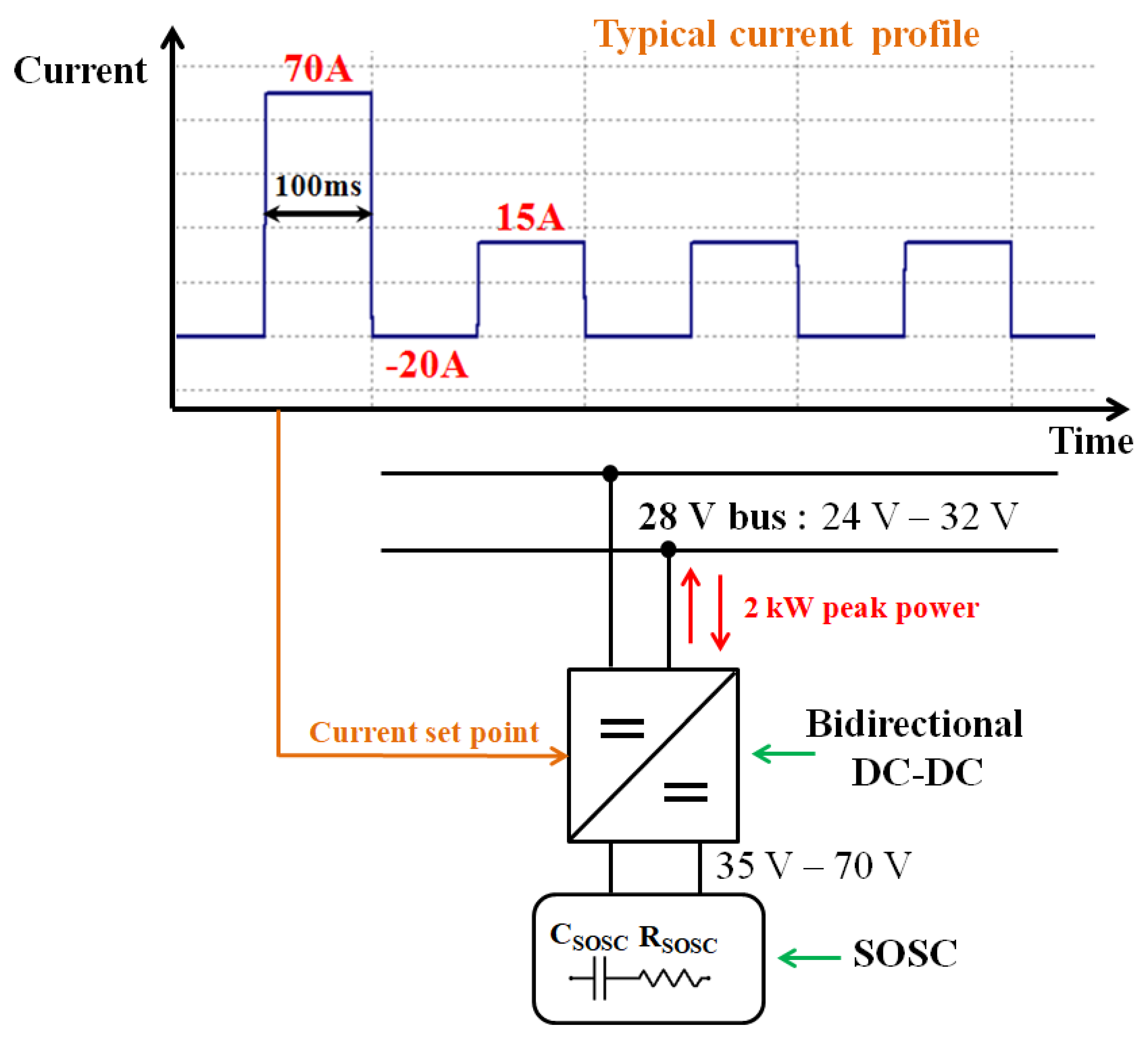
The aim of the proposed DC-DC converter is to manage the energy flow between two energy sources, being in the specific case a Stack Of Supercapacitors (SOSC) and a DC voltage bus, as highlighted in
Figure 1, showing the power system architecture. A typical current profile, required from the bus section, is highlighted as well: the positive current values correspond to a SOSC discharge, whereas the negative ones correspond to a SOSC recharge. The maximum required current value is 70 A, which is equivalent to a maximum rated power of 2 kW for a nominal DC bus voltage equal to 28 V.
2.1. Energy Sources Model
The SOSC voltage lies in the range 35 V–70 V, whereas the nominal DC bus voltage is 28 V. In
Table 1 the SOSC parameters and voltage range are reported, where
CSOSC and
RSOSC are the SOSC equivalent capacitance and resistance. The reported values arise from the considered specific stack, which is supposed to be a 26s11p (26 series–11 parallel) connection of 2.7 V 10 F 35 mΩ ultracapacitor cells (Maxwell Technologies, San Diego, CA, USA).
Being equal to the product between CSOSC and RSOSC, the SOSC charge/discharge time constant is equivalent to hundreds of ms, so that the SOSC can be considered as a DC power source with respect to a converter switching frequency in the order of tens-of-kHz. For this reason the proposed converter can be analyzed and designed as an actual DC-DC converter.
In
Table 2 the DC bus specifications concerning the voltage level are reported.
2.2. Full Bridge Converter Analysis
In
Figure 2, the schematic of the proposed Full Bridge Converter (FBC) is shown. The FBC is an insulated topology, featuring a transformer between the sections connected to the DC voltages
V1 and
V2, representing the SOSC and the bus respectively. As far as the transformer is concerned,
L1 and
Lm are the equivalent primary leakage and magnetizing inductances respectively, whereas
n:m is the turns ratio. Each of the H-bridges in the primary and in the secondary side of the transformer consists of four switches, in this specific case four enhancement n-channel MOSFETs—the primary side H-bridge consists of M1-M2-M3-M4, whereas the secondary side one consists of M5-M6-M7-M8. In this network therefore energy can flow in both directions, either from
V1 to
V2 or from
V2 to
V1—in the first case the primary H-bridge acts as an inverter and the secondary one as a rectifier, in the second case the H-bridges play the opposite roles.
If a voltage source is connected to V1 port and a load is connected to V2 port, the proposed converter implements a step-down operation.
The primary and secondary H-bridges can therefore be referenced as High-Side Bridge (HSBridge) and Low-Side Bridge (LSBridge).
L2 is the converter inductor, placed in series with the LSBridge.
2.3. Possible Modulation Techniques
Two possible modulation schemes have been investigated on the proposed FBC, as shown in
Figure 3 and
Figure 4,
Vgn being the logic level applied to the gate-source voltage of the MOSFET Mn—the Pulse Width Modulation (PWM) and the Phase Shift Modulation (PSM).
Figure 3 shows the PWM scheme—M1 and M4 gate signals are in phase, as well as M2 and M3 gate signals and a phase difference occurs between the diagonals M1–M4 and M2–M3; the secondary-side gate signals are obtained by logical negation (NOT) of the primary-side signals, as highlighted in the figure. The on-time of each HSBridge switch is
DTs, where
D is the duty-cycle and
Ts the switching period, being the duty-cycle limited to less than 50% in order to avoid short-circuit at the primary side.
As highlighted by the modes of operation, if D goes higher than 50%, the time windows T2 and T4, corresponding to the L2 discharge towards short circuit, would be deleted, thus avoiding a proper converter working; moreover, the time windows T1 and T3 would be in overlap, thus leading to an undesirable short circuit on V1.
Figure 4 shows the PSM scheme—M1 and M2 are always in phase opposition, as well as M3 and M4; a phase difference, corresponding to the duty-cycle
D, occurs between them. The PWM, therefore, is converted into a phase shift modulation.
At the same way as in the PWM, the duty-cycle D is limited to less than 50% in order to avoid open-circuit at the secondary side, which could lead to voltage spikes due to the inductance L2.
As highlighted by the modes of operation, if D goes higher than 50%, the time windows T2 and T4, corresponding to the L2 discharge towards short circuit, would be deleted, thus avoiding a proper converter working, such as in the PWM mode; moreover, the time windows T1 and T3 would be in overlap, thus leading to an undesirable open circuit on L2.
The PSM scheme has been preferred to the PWM, since the PWM scheme involves higher switching power losses, due to the Zero Voltage Switching (ZVS) condition which is reached in the PSM.
The proposed converter aims at the regulation of the power in terms of both amount and direction.
Considering that V1 and V2 are two DC voltage sources—a Stack Of Supercapacitors and a DC bus respectively—the power regulation is therefore consisting in a current regulation.

 ,
, 


