Article

Study on Boost Converters with High Power-Density for Hydrogen-Fuel-Cell Hybrid Railway System

1
Department of Electrical Engineering, Incheon National University, 119, Academy-ro, Yeonsu-gu, Incheon 22012, Korea
2
Department of Electrical Engineering, Myongji University, Yongin 17058, Korea
*
Author to whom correspondence should be addressed.
Electronics 2020, 9(5), 771; https://doi.org/10.3390/electronics9050771
Submission received: 14 April 2020 / Revised: 25 April 2020 / Accepted: 6 May 2020 / Published: 8 May 2020
(This article belongs to the Section Power Electronics)

Abstract

:
Step-up DC/DC converters are needed generally for the hydrogen-fuel-cell (HFC) hybrid railway system since the HFC has difficulty directly generating a high link voltage of over 1500 V for the high-power capacity inverter to drive the traction motor in the vehicle. These step-up DC/DC converters demand a high conversion efficiency with low weight and volume, due to the limited space in vehicle. In this paper, step-up DC/DC converters are presented and are evaluated for the HFC hybrid railway system. By choosing the interleaved boost converter and the 3-level boost converter as promising candidates, characteristics and features of both converters are presented through the analysis of the operational principles. In addition, the optimal design methods and results of boost inductor, output capacitor, and power semiconductor devices are presented based on theoretical analysis and a real design specification for the HFC hybrid railway system. Moreover, an optimal digital control design in terms of dynamic current response and reliability, such as current-balance or voltage-balance controls, is presented in this paper. In order to verify the analysis and design results, prototypes of both converters with the 600 V input and 1200 V/20 kW output specifications are constructed and the performance of the interleaved and 3-level boost converters are demonstrated through the experimental results. The experimental results show that the 3-level boost converter is more suitable for the HFC hybrid railway system in the sense of efficiency, power-density, and dynamic current response.

1. Introduction

Nowadays, as railway technologies have been researched and developed, there are many attempts to incorporate and integrate elemental technologies with other industries. In order to overcome the depletion of fossil energy and environmental problems, the research has been especially conducted in various ways to combine the renewable energy as an energy source for the propulsion systems in railway vehicles. In consideration of the limited space and weight in railway vehicles, stability of the fuel supply, and other features such as that there is no power supply from the outside of the railway vehicle, it is analyzed that the bio-diesel and hydrogen-fuel-cell system are adequate among the renewable energy sources for railway vehicles. However, in reality, it is difficult to apply bio-diesel as an energy source for the propulsion system of eco-friendly railway vehicles due to environment and supply stability issues.
Meanwhile, the hydrogen-fuel-cell system has been gaining attention since it not only shows more than 50% efficiency, which is higher than the 30% efficiency of the existing fossil energy, but also has low noise and vibration. In addition, due to the fuel tank in the hydrogen-fuel-cell system, a continuous power supply is possible and this makes the system easier to build than other renewable energy sources. As a result, hydrogen-fuel-cell systems are already commercialized in eco-friendly vehicles and buses. In the railway system, the technologies for applying the hydrogen-fuel-cell as an energy source have been rapidly researched and developed, and the Railway Authority in Germany has finally approved the commercial operation of the hydrogen-fuel-cell railway vehicle developed by Alstom [1,2].
This hydrogen-fuel-cell system appears to have many advantages, but there are also several disadvantages such as a high cost, low dynamic performance, and the difficulty to store and reuse the regenerating braking energy. In order to relieve theses disadvantages, the energy storage devices such as the super capacitor and battery are adopted as shown in Figure 1. As a result, it is possible to utilize the hydrogen-fuel-cell system for eco-friendly vehicles, buses, and railway vehicles, which require fast dynamic performance and energy saving through regenerative braking.
Figure 1 presents the hybrid hydrogen-fuel-cell propulsion system which uses both the hydrogen-fuel-cell and battery as the energy source for the propulsion of the railway vehicle. This hybrid propulsion system requires a step-up converter between the hydrogen-fuel-cell and battery because the fuel-cell generates a relatively low voltage, which has difficulty driving the high voltage propulsion motor. Moreover, the high cost of the hydrogen-fuel-cell makes it difficult to supply driving energy for the traction motor, so in order to achieve the stable power supply and reuse the regenerating braking energy, an auxiliary battery is added and it is connected to the input side of the inverter as shown in Figure 1.
For the voltage step-up operation, the conventional boost converter shown in Figure 2 has been widely used because of the continuous input current and high voltage conversion ratio. In addition, the simple structure of the boost converter is advantageous in a railway vehicle system with limited space and weight, unlike the general railway system due to the hydrogen-fuel-cell and battery mounted on the railway vehicle. However, the boost converter cannot achieve the zero-voltage-switching (ZVS) operation, so it results in high turn-on and turn-off switching losses and reverse-recovery loss. In addition, a high voltage-rating switch and diode that features a low switching speed should be used for the boost converter since the voltage stresses on the switch and diode are larger than the output voltage, which is nearly 1500 V in the HFC railway system. Furthermore, these high voltage stresses on devices cause the considerably high switching loss, resulting in the low switching frequency. Since the switching frequency is proportional to the volume of the inductor and capacitor, consequently, the size of the inductor and capacitor is considerably larger, and it results in poor power-density of the step-up DC/DC converter.
In order to make up for the drawbacks of the conventional boost converter, the interleaved and three-level boost converter have been developed and widely used for the hybrid hydrogen-fuel-cell railway system. These converters show low switching loss and can operate with higher switching frequency compared with the conventional boost converter [3,4,5]. In this paper, both interleaved and three-level boost converters thoroughly review for the high efficiency and power density through the analysis in various ways. The operation principles of both converters are illustrated and presented, and the design consideration, such as the switches and didoes selection and ripple analysis of input current/output voltage, are conducted as following sections. Finally, by constructing the 600 V input and 1200 V/20 kW output prototypes and comparing the efficiency and volume, the validity of both converters is verified.

2. Operational Principle of Boost Converters for Hydrogen-Fuel-Cell Hybrid Railway System

Figure 3 describes the circuit diagrams of the interleaved boost converter and three-level boost converters, which are the promising topologies for the hydrogen-fuel-cell hybrid railway system. In order to analyze the operation of both converters, the operation principles are illustrated corresponding to the operational duty range, i.e., D ≤ 0.5 and D > 0.5, since the operation of the boost converters varies when the duty-ratio is over 0.5.

2.1. Interleaved Boost Converter

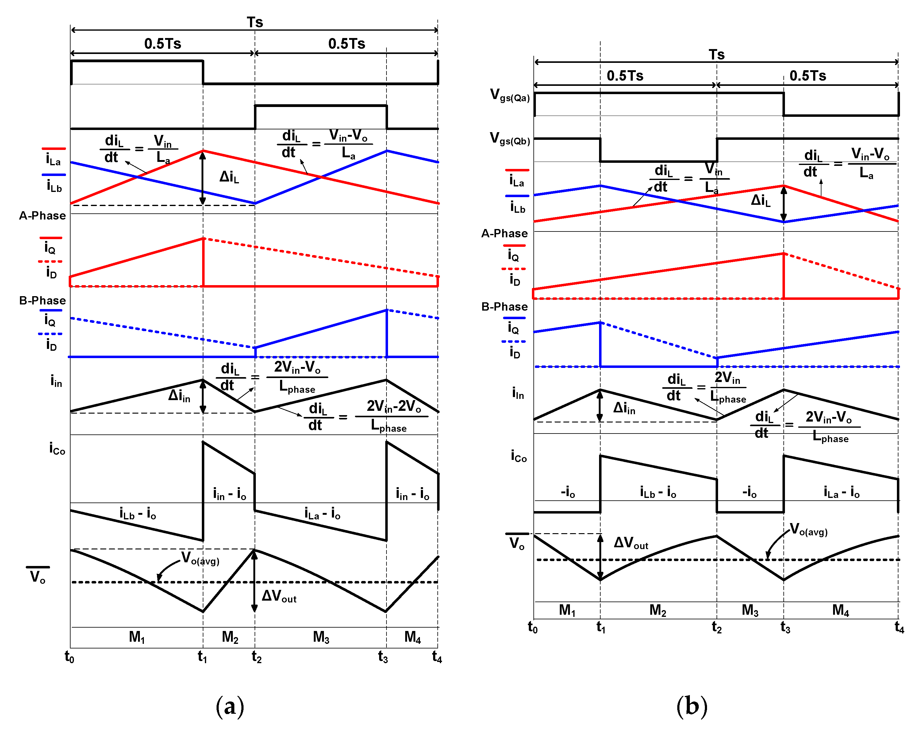
Figure 3a and Figure 4 shows the circuit diagram of the interleaved boost converter and its operation key waveforms according to the operating duty-ratio. This interleaved boost converter normally consists of the two switches (Qa, Qb), two diodes (Da, Db), two inductors (La, Lb) and only one output capacitor(CO), and two boost converter are connected parallel as shown in Figure 3a. Due to the parallel connected boost converters, the duty-ratio of Qa and Qb is required to be equal to regulate the output voltage. In addition, in order to achieve the reduced input current ripple by cancelation of the inductor currents, the Qa and Qb are controlled with a 180°phase difference. As a result, despite the low switching frequency of the interleaved boost converter compared with that of the conventional boost converter, it is possible to achieve almost the same input current ripple with high efficiency. Meanwhile, the operation of the interleaved boost converter varies according to the operating duty-ratio range. Thus, the operation of the interleave boost converter during D ≤ 0.5 and D > 0.5 should be analyzed in the following subsections. For the sake of the analysis, several assumptions are made as follows:
(1)
all parasitic components except for those specified in Figure 3a are ignored;
(2)
the output capacitor (CO) is large enough to be considered as a constant output voltage (VO);
(3)
the inductances of every inductor are equal, and each average inductor current is well controlled and balanced;
(4)
Only two modes among four modes in one switching cycle are explained and analyzed since the two modes are symmetric with the other operational modes.

2.1.1. Operation of Interleaved Boost Converter during D ≤ 0.5

Figure 4a illustrates the operational key waveforms of the interleaved boost converter under 0.5 duty-ratio, and each mode is explained corresponding to its topological state as represented in Figure 5.
Mode 1 [t0t1, Figure 5a]: In this mode, Qa is turned on at t0, and Qb maintains the turn-off state. Since the input voltage (Vin) is applied to La, the inductor current of La (iLa) increases linearly with Vin/La slope while La stores the energy. Meanwhile, Vin-VO is applied to Lb. Thus, the inductor current of Lb (iLb) decreases linearly with (VinVO)/Lb slope, and the stored energy in Lb is discharged to the output through D2. Since the two boost converters are connected in parallel to the input, the sum of iLa and iLb flows from the input.
Mode 2 [t1t2, Figure 5b]: At t1, Qa is turned off, so both switches Qa and Qb are turned off for mode 2. In this mode, both inductors discharge the stored energies to the output through the diodes Da and Db. This means that VinVO is applied to La and Lb, and both iLa and iLb decrease linearly with (VinVO)/Lb slope. As a result, the input current (iin) decreases with 2(VinVO)/Lb slope. At the end of mode 2, Qb is turned on, and the switching loss of Qb and reverse recovery loss of Db occur due to current transition at the switch turn-on instant. After this, the other operational modes are symmetric with mode 1 and mode 2.

2.1.2. Operation of Interleaved Boost Converter during D > 0.5

Figure 4b show the key waveforms of the interleaved boost converter with over 0.5 duty-ratio in one switching cycle.
Mode 1 [t0t1, Figure 6a]: In this mode, Qa is turned on at t0 causing the switching and reverse recovery losses, and both Qa and Qb maintain the turn-on state for this mode. Since both switches are turned on, the input voltage (Vin) is applied to La and Lb and both inductors store the energy, both iLa and iLb increase linearly with Vin/La slope. At that time, the input current, which is the sum of iLa and iLb, also linearly increases with 2Vin/La slope, and CO discharges the current as much as the output current.
Mode 2 [t1t2, Figure 6b]: At t1, Qb is turned off, and Qa maintains the turn-on state during mode 2. In this mode, Vin is still applied to La and iLb linearly increases with Vin/La slope, storing the energy. On the other hand, the applied voltage on Lb becomes VinVO and Lb discharges the stored energy, resulting in the linearly decrease of iLb with (VinVO)/Lb slope. Since the output voltage during D > 0.5 is much larger than that during D ≤ 0.5, ΔiLb during this mode is larger than ΔiLa and iin linearly decreases by the difference between ΔiLb − ΔiLa, as depicted in Figure 4b. At t2, Qb is turned on resulting in the switching and reverse recovery losses and the other modes, which are almost the same as mode 1 and mode 2, begin.

2.2. Three-Level Boost Converter

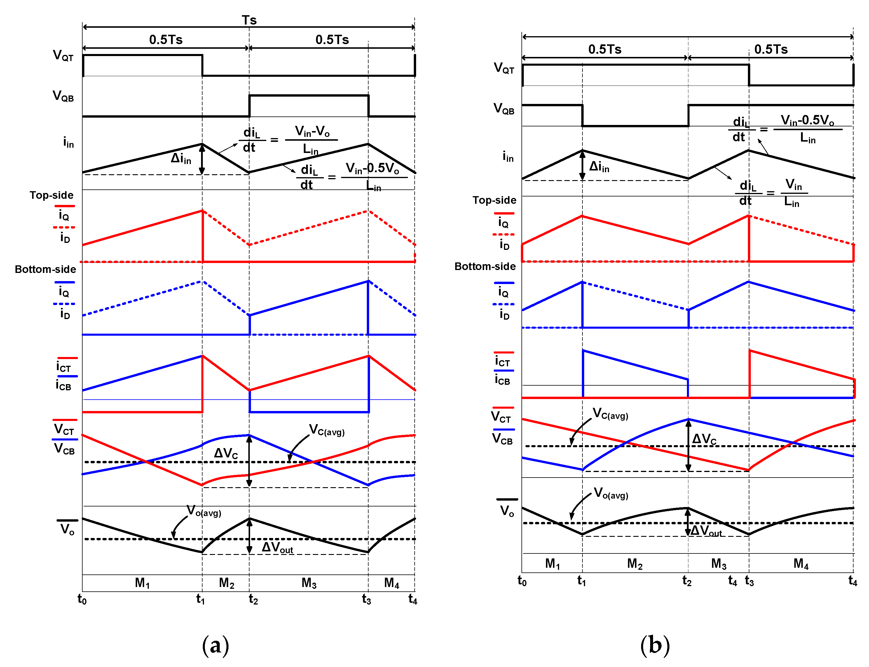
Figure 3b shows the circuit diagram of the three-level boost converter, and according to duty-ratio range, the operational waveforms are illustrated as shown in Figure 7. Similar to the interleaved boost converter, the three-level boost converter also consists of two switches (QT, QB) and two diodes (DT, DB). However, the three-level boost converter utilizes single input inductor (Lin) rather than using two inductors, and adopts two output capacitors (CT, CB) to generate three-level voltage. The three-level boost converter also controls QT and QB with 180° phase shift to minimize Δiin, so the operation of the three-level boost converter also can be divided in accordance with the duty range such as D ≤ 0.5 and D > 0.5. For the sake of the analysis, several assumptions are made as follows:
(1)
all parasitic components except for those specified in Figure 3b are ignored;
(2)
the duty-ratio of QT (D1) is the same as the duty-ratio of QB (D2);
(3)
all output capacitance of capacitors (CT, CB) are equal, and the voltages of capacitors (VCT, VCB) are well balanced and the same as 0.5VO;
(4)
only two modes among four modes in one switching cycle are explained and analyzed since the two modes are symmetric with the other operational modes.

2.2.1. Operation of Three-Level Boost Converter during D ≤ 0.5

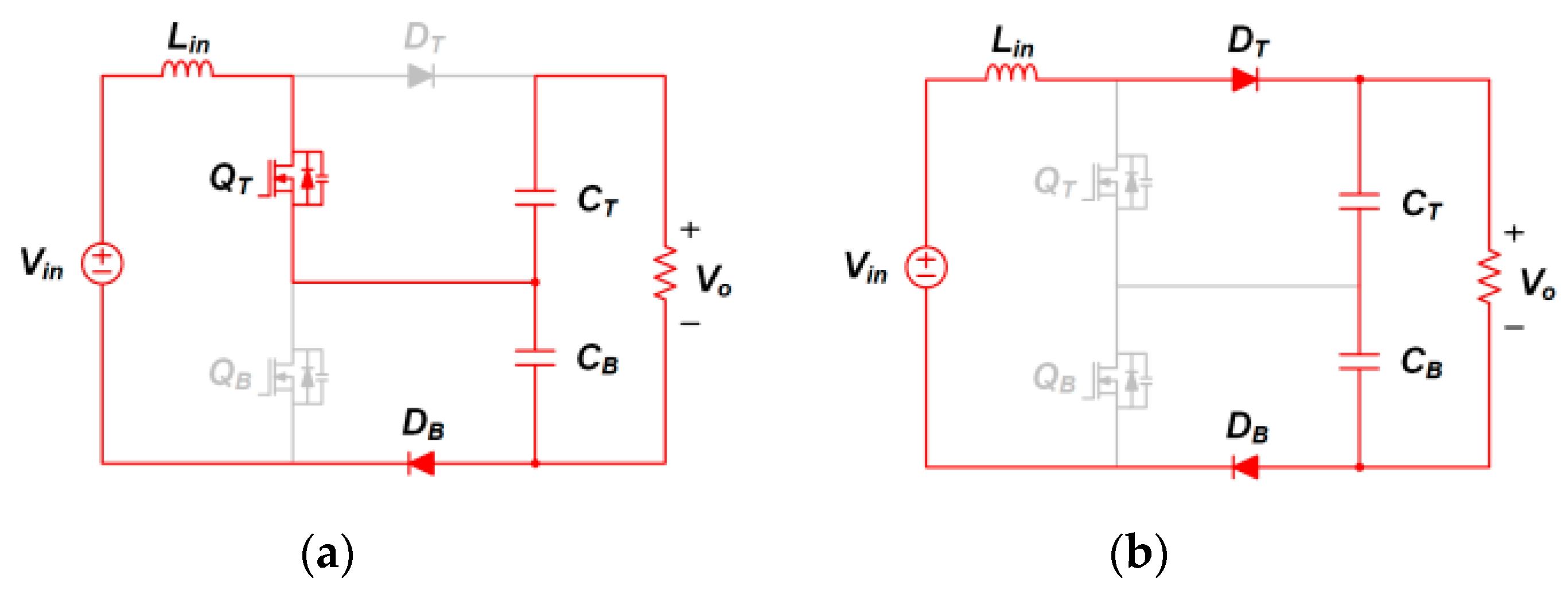
Figure 7a shows the operational key waveforms of the three-level boost converter when it operates under 0.5 duty-ratio, and each mode is explained precisely.
Mode 1 [t0t1, Figure 8a]: QT is turned on at t0, and QB maintains the turn-off state in this mode. In this mode, Vin − 0.5VO is applied to Lin, so the inductor stores the energy and transfers the power to the output through CB. As a result, the input and inductor current (iin) increases linearly with Vin − 0.5VO/Lin slope because 0.5VO is smaller than Vin because of its small duty-ratio.
Mode 2 [t1t2, Figure 8b]: At t1, QT is turned off, so both switches QT and QB are turned off and DT conducts during mode 2. In this mode, VinVO is applied to Lin, and the stored energy in Lin is discharged to the output through DT. Due to this, iin decreases linearly with (VinVO)/Lin slope. At t2, QB is turned on causing the switching loss of QB and reverse recovery loss of DB.

2.2.2. Operation of Three-Level Boost Converter during D > 0.5

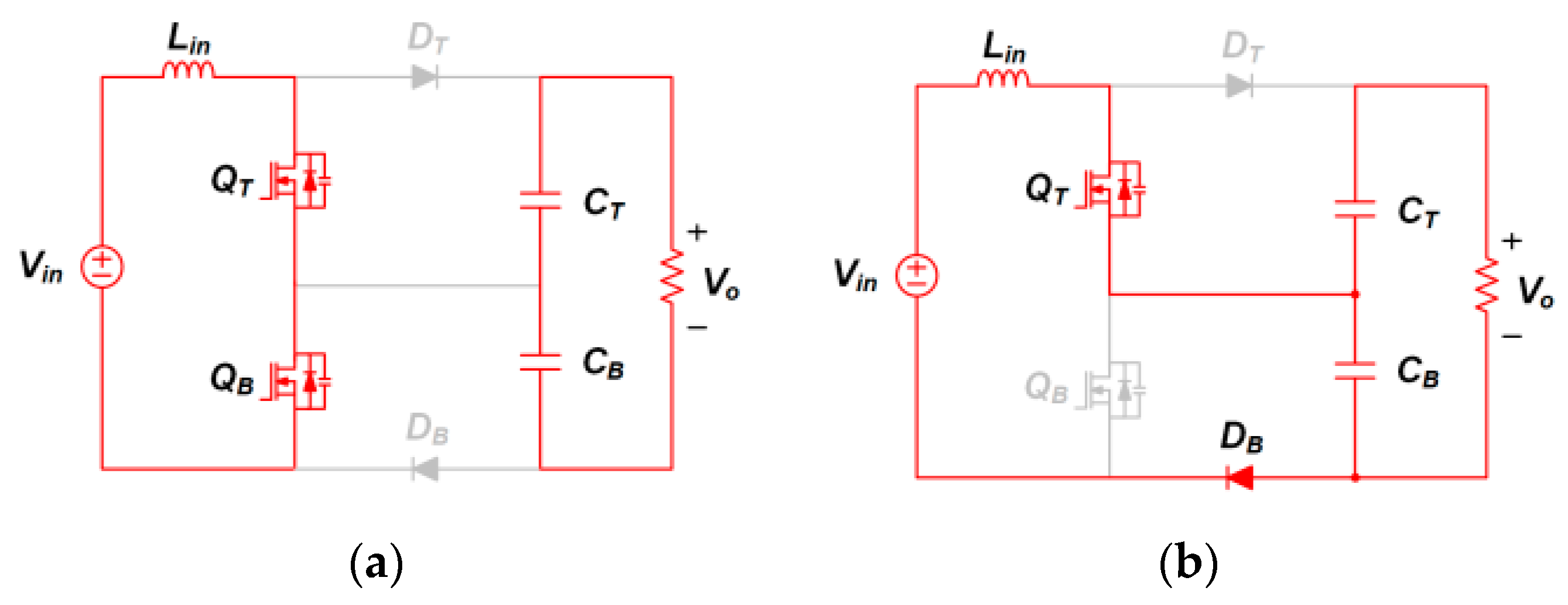
Figure 7b presents the operational waveforms of the three-level boost converter when the duty-ratio is over 0.5, and each mode shown in Figure 9 is explained as follows.
Mode 1 [t0t1, Figure 9a]: In this mode, QT is turned on at t0 causing the switching loss of QT and reverse recovery loss of DT, and both QT and QB maintain the turn-on state during this mode. Since both switches are turned on, the input voltage (Vin) is applied to Lin and iin increases linearly with Vin/Lin slope storing energy. At this time, the output capacitances discharge the current as much as the output current.
Mode 2 [t1t2, Figure 9b]: At t1, QB is turned off, and QT is still turned on. In this mode, Vin − 0.5VO is applied to Lin, and iin linearly decreases with (Vin − 0.5VO)/Lin slope. In addition, the stored energy in Lin is discharged to the output through DB. This is because that the high duty ratio over 0.5 results in the high output voltage which is twice as large as the input voltage.

3. Analysis and Design Consideration

Table 1 shows the input and output specifications of the prototype DC/DC converters for the hydrogen-fuel-cell hybrid railway system. Based on these specifications, the dc conversion ratio, boost inductors, output capacitors, switches, and diodes are designed and chosen. Then, switching, conduction, and core losses are analyzed and compared between the interleaved and three-level boost converters in accordance with the design results. By analysis and design consideration, the validity of the two DC/DC converters for hydrogen-fuel-cell hybrid railway system will be verified.

3.1. DC Conversion Ratio of Interleaved and 3-Level Boost Converters

The DC conversion ratio of the interleaved boost converter and three-level boost converter can be achieved from the voltage second balance of inductors as shown in Figure 10 and Figure 11. Considering the operating duty range, the DC conversion ratio under 0.5 duty ratio and over 0.5 duty ratio of the interleaved boost converter can be derived as follows, and those are the same as the DC conversion ratio of the conventional boost converter:
< v L ( t ) > | D 0.5 = V i n D T S + ( V i n V O ) ( 1 D ) T S ,
< v L ( t ) > | D > 0.5 = V i n D T S + ( V i n V O ) ( 1 D ) T S ,
V O = 1 1 D V i n .
The voltage second balance of the three-level boost converter under 0.5 duty-ratio and over 0.5 duty-ratio can be represented as in Equations (4) and (5), respectively:
< v L ( t ) > | D 0.5 = ( V i n 0.5 V O ) D T S + ( V i n V O ) ( 0.5 D ) T S ,
< v L ( t ) > | D > 0.5 = ( V i n ) ( D 0.5 ) T S + ( V i n 0.5 V O ) ( 1 D ) T S .
From Equations (4) and (5), the DC conversion ratio of the three-level boost converter is represented as in Equation (6), and it is equal to the conventional boost converter:
V O = 1 1 D V i n .

3.2. Boost Inductor Design Consideration

In the interleaved boost converter operating with under 0.5 duty-ratio, ΔiLa, ΔiLb, and Δiin can be derived based on the applied voltage on the boost inductors:
Δ i L a = Δ i L b = V i n D T S L a = V i n D T S L b = V i n D T S L ,
Δ i i n = ( 2 V i n V O ) D T S L ,
where the inductance, L is equal to La and Lb. From Equation (8), L of the boost inductors can be derived as below, taking into account the input, output, and current ripple specifications.
L = ( 2 V i n V O ) D T S Δ i i n .
If the interleaved boost converter operates over 0.5 duty-ratio, ΔiLa, ΔiLb, Δiin, and L can be represented as follows:
Δ i L a = Δ i L b = V i n D T S L a = V i n D T S L b = V i n D T S L ,
Δ i i n = 2 V i n ( D 0.5 ) T S L ,   L = 2 V i n ( D 0.5 ) T S Δ i i n .
ΔiLin, which is the same as Δiin and Lin of the thee-level boost converter when the converter operates under 0.5, can be derived as follows from the inductor voltage and current relationship:
Δ i L i n = Δ i i n = ( V i n 0.5 V O ) D T S L i n ,   L i n = ( V i n 0.5 V O ) D T S Δ i L i n .
While the three-level boost converter operates over 0.5 duty-ratio, current ripples and Lin can be expressed as bellow:
Δ i L i n = Δ i i n = V i n ( D 0.5 ) T S L i n ,   L i n = V i n ( D 0.5 ) T S Δ i L .
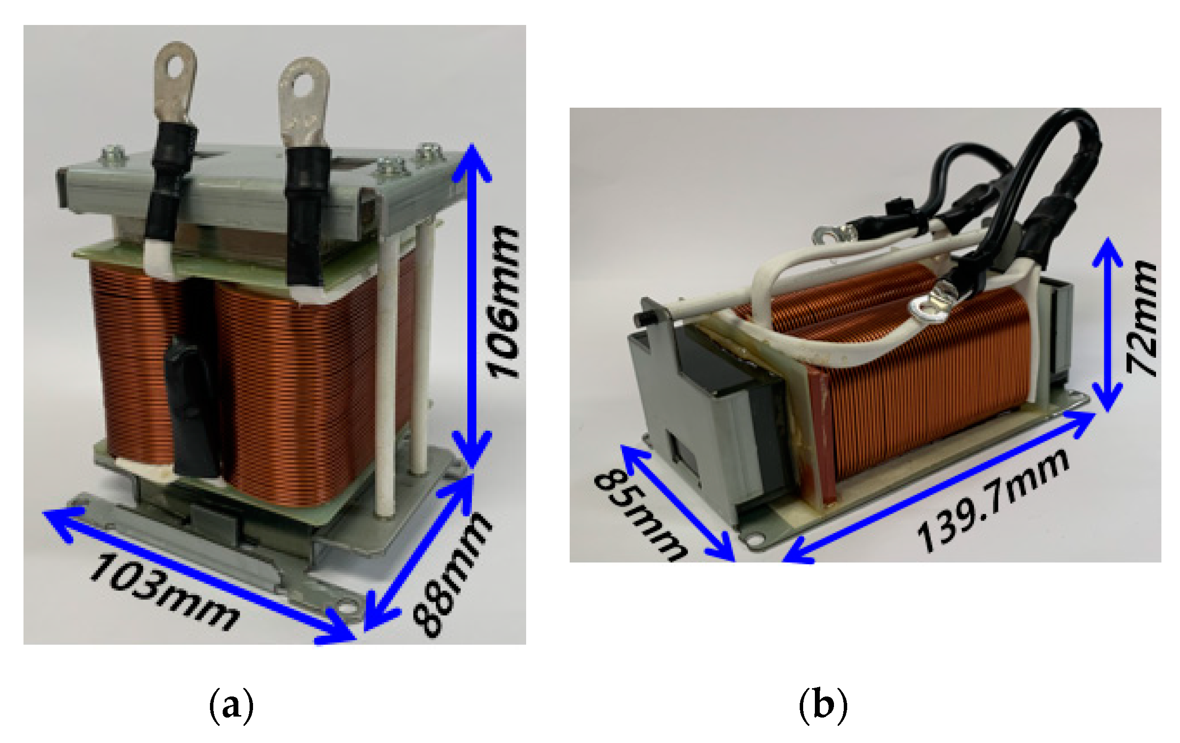
Since Δiin of the interleaved and three-level boost converters must be satisfied that the current ripple condition that is 10% of the rated current under entire output conditions, the inductances of both converters are designed through the consideration of the worst case conditions, e.g., 1008 V output and full load conditions. Table 2 shows the design results of the inductors, and as represented in Table 2, the inductance of the three-level boost converter is significantly lower than that of the interleaved boost converter. This means that the three-level boost converter can achieve a high power-density compared with the interleaved boost converter due to the low inductance and number of the inductor. The detailed design results about the inductor core, wire, and number of turns are also presented in Table 2. In order to design the inductor, the area-product (AP), which is product of the core area (AC) and winding area (AW), are used in this paper, and it can be represented as in Equation (14):
A P = A C A W = L I L , p e a k I L , r m s B M K U J ,
where IL,peak and IL,RMS are the peak and RMS (root-mean-square) inductor currents, BM is the maximum flux density, KU means the utility factor of winding, and J is the current density of the wire.
The interleaved boost converter utilizes two phases and each phase has series connected inductors, so the inductor current is half that of the inductor current of the three-level boost converter. However, the inductance of the interleaved boost converter is almost seven times larger than that of the three-level boost converter, so the total AP of LA and LB in the interleaved boost converter is approximately three times higher than the AP of Lin in the three-level boost converter, assuming the same BM and J. Therefore, as shown in Table 2, due to a small AP the three-level boost converter can reduce the volume of the inductor and can achieve a high efficiency through the reduced core and conduction losses.

3.3. Output Capacitor Design Consideration

There is little difference with the output capacitor design between both converters. As shown in the circuit diagrams, the interleaved boost converter utilizes the high voltage capacitor. Meanwhile, the three-level converter adopts series connected output capacitors by using the low voltage capacitor, as illustrated in Figure 3b. In order to compare the design results such as capacitance and volume of the output capacitor in both converters, the required capacitance for each converter should be derived and achieved from the voltage ripple specification.
In the interleaved boost converter, when the converter operates under 0.5 duty-ratio, ΔVO and CO can be obtained as follows considering the current-second balance of the output capacitor shown in Figure 4:
Δ V O = ( I L I O ) D T S C O ,   C O = ( I L I O ) D T S Δ V O .
If the interleaved boost converter operates over 0.5 duty-ratio, ΔVO and CO can be expressed as follows:
Δ V O = I O ( D 0.5 ) T S C O ,   C O = I O ( D 0.5 ) T S Δ V O .
On the other hand, due to the series connected output capacitor, ΔVO is the sum of the output capacitor voltages, i.e., ΔVCT + ΔVCB as shown in Figure 7. As a result, ΔVO, CT, and CB, when the three-level boost converter operates under 0.5 duty-ratio, can be represented as bellows:
Δ V C T = Δ V C B = I O ( 1 D ) T S C ,
Δ V O = ( 2 I O I L ) D T S C ,   C = ( 2 I O I L ) D T S Δ V O ,
where C is equal to CT and CB. Assuming that the three-level converter operates over 0.5 duty-ratio, considering the current-second balance, ΔVO, CT, and CB also can be expressed as follows:
Δ V C T = Δ V C B = I O ( 1 D ) T S C ,
Δ V O = 2 I O ( D 0.5 ) T S C ,   C = 2 I O ( D 0.5 ) T S Δ V O .
The requirement of the output voltage ripple is 1% of the rated voltage as presented in Table 1. Thus, the capacitance of the both converters to meet this requirement irrespective of output voltage variations. Table 3 expresses the design results in consideration of the worst-case condition that shows maximum capacitance value. As shown in Table 3, the capacitance of the interleaved boost converter requires almost twice that of the three-level boost converter. In addition, the voltage stress on the capacitor of the three-level converter is half of that of the interleaved converter. Although the three-level boost converter adopts series connected output capacitors, due to low voltage stress it is more attractive for the high step-up applications. The design results of the capacitor are represented in Table 3, including the voltage and current rating and number of capacitors considering the maximum voltage and RMS current of the capacitor.

3.4. Voltage and Current Stresses on Switches and Diode

The voltage and current stresses on switches and diodes of both the converters are shown in Table 4. As shown in Table 4 and as mentioned before, the three-level boost converter shows half the voltage stresses on devices compared with those of the interleaved boost converter, due to the three-level structure. Since the railway vehicle system in Korea requires more than 50% voltage stress margin for high stability, over 2000 V voltage rating switching devices should be applied to the interleaved boost converter. Thus, the interleaved boost converter must utilize IGBT (insulated gate bipolar transistor) rather than SiC (Silicon-carbide) devices because of the under 1700 V voltage rating SiC devices that have been developed and commercialized. Meanwhile, SiC devices can be used for the three-level boost converter, so that the dramatically reduced switching losses in the three-level boost converter can be achieved due to the ultra-fast switching speed and approximately zero reverse recovery of SiC devices.
In terms of the voltage stress, the currents on devices in the three-level boost converter are approximately twice as larger as those of the interleaved boost converter, and this large current of the three-level boost converter causes the high conduction loss. Although the conduction losses on devices of the three-level boost converter are larger than those of the interleaved boost converter, the switching losses of the devices are large compared with conduction losses, so the total losses of the switching devices of the three-level converter is much smaller than those of the interleaved boost converter because it shows low voltage stresses and can apply SiC devices.
The design results of the switches and diodes are also represented in Table 4; IGBTs are adopted to the interleaved boost converter, and SiC-MOSFETs are used as the switch of the three-level boost converter. In addition, phase-leg modules are generally adopted for the high power hydrogen-fuel-cell system, i.e., 1200 V input and 1500 V/200 kW output, the output diodes of both converters are implemented by using the anti-parallel diode in IGBT and SiC-MOSFET.

3.5. Loss Comparison between Interleaved and 3-Level Boost Converters

Table 5 shows the design results of both boost converters. In order to compare the power losses, the core and copper losses of inductors, and switching and conduction losses of switches and diodes are analyzed [6]. The capacitance ESR (equivalent series resistance) loss be ignored since this loss is small enough to be negligible.
In order to achieve the copper loss (Pcopper) and core loss (Pcore) of the inductors (Pcopper), the wire resistance (Rwire) can be derived as (21), and Pcopper and Pcore can be obtained as follows:
R w i r e = M L T N [ 1.724 × 10 6 w i r e A e { 1 + 0.00393 ( T 20 ) } ] ,
P c o p p e r = R w i r e I r m s 2 ,
P c o r e = a B b f c 10 3 ,
where MLT is the mean length turn, N means turns of inductor, wireAe is the wire effective area, B is the half of flux density variation (ΔB/2), VC means the core volume, and a, b, and c means core loss factor from datasheet [7].
The conduction and switching losses of the switches including the output parasitic capacitance, gate charge, and switching turn-on/off losses can be derived as bellow:
P c o n = I R M S 2 R d s ( o n ) ,
P S w i c h i n g = P C O S S + P Q g + P o n + P o f f = C O S S V p e a k 2 f s w 2 + V g s Q g f s w + 1 2 ( t r V o n I o n + t f V o f f I o f f ) f s w ,
where Rds(on) means the on-resistance, Coss is the parasitic capacitance, Qg is the gate charge, VGS is the gate-source voltage, tr and tf mean the rising and falling time of the switch, and Von, Voff, Ion, and Ioff mean the turn-on/off instant voltages and currents on switch. The diode conduction and reverse recovery losses can be obtained as (26) and (27) by using the diode forward voltage drop (VF) and reverse recovery charge (Qrr):
P V F = V F I D ,
P Q r r = Q r r V D f S .
In terms of the diode losses, the reverse recovery loss can be dramatically reduced when the SiC-schottky diode that shows the almost zero reverse recovery is adopted for the boost converter.
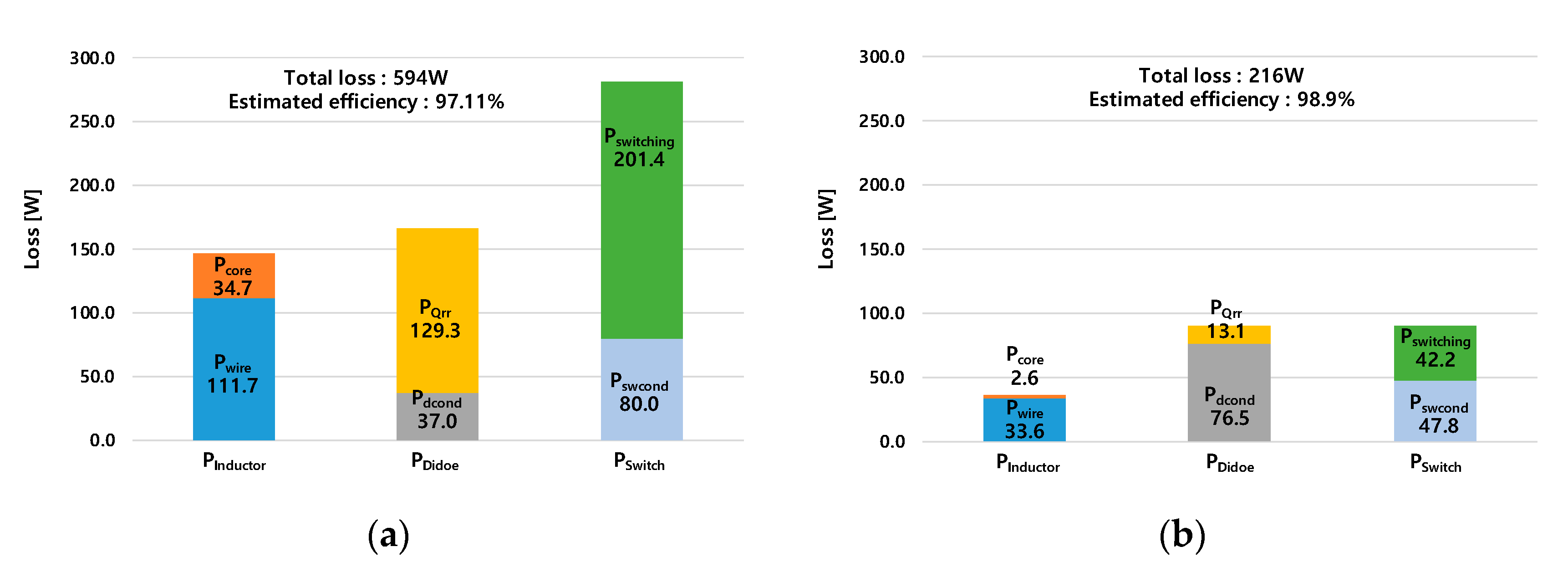
Figure 12 shows the comparison of the estimated power losses in the interleaved and three-level boost converters based on parameters shown in Table 6 which are derived from datasheets of switches and above equations. As illustrated in Table 5, the interleaved boost converter requires a total of four inductors, which consist of series-connected inductors per phase because of the considerably high AP. Meanwhile, the three-level converter only utilizes a single inductor. This is because that the AP of inductor of the three-level converter is almost 1/3 times lower than that of the interleaved boost converter as aforementioned. As a result, as shown in Figure 12, the total inductor loss of the three-level boost converter is almost 1/4 times lower than that of the interleaved boost converter, and it results in a high efficiency and power density of the three-level boost converter.
In the case of the switches and diodes, the switches and diodes are connected in parallel because of the heat dissipation of devices. The three-level boost converter uses a total of four switches, and each QT and QB consists of parallel-connected two switches. On the contrary, in the interleaved boost converter, each QA and QB is composed of parallel-connected four switches, so the interleaved boost converter utilizes a total of eight switches. This is because that IGBTs in the interleaved boost converter have a low switching speed and it induces significantly increased switching losses, as shown in Figure 12. As a result, more switches must be connected in parallel for the interleaved boost converter compared with the three-level boost converter, as represented in Table 5. In accordance with this tendency, the total switching losses of the interleaved boost converter is more than four times larger compared with the three-level converter. Meanwhile, due to the high average current and high conduction losses of diodes in the three-level boost converter, four diodes are connected parallel in the three-level booster converter. However, only two diodes which are connected parallel are used for the interleaved boost converter. As a result, conduction losses of diodes in the three-level boost converter is two times larger than those in the interleaved boost converter. Despite the large conduction losses of the three-level boost converter, the total losses of diodes in the three-level boost converter are considerably lower than those of the interleaved boost converter because of the antiparallel diode of SiC MOSFET in the three-level boost converter, which shows almost zero reverse recovery resulting in minimized reverse recovery loss compared with that of the antiparallel diode in IGBT which is used as the diode in the interleaved boost converter.
Through the loss comparison, the inductor, switch, and diode losses are theoretically analyzed and explained in this subsection. As above mentioned, both converters have the same number of switching devices such as switches and diodes. However, the three-level boost converter shows considerably lower total losses of the switching devices by adopting the SiC devices. In addition, the three-level boost converter only utilizes a single inductor, which is closely related with the small volume and low losses of inductor, while two series-connected inductors per phase for the interleaving structure are required in the interleaved boost converter. Therefore, although both converters are promising for high-output and high-power applications such as the hydrogen-fuel-cell hybrid railway system, the three-level boost converter is more suitable and a good candidate for this application.

4. Experimental Results

In order to verify the validity of the analysis of both converters, prototypes with Vin = 600 V, VO = 1000 V–1360 V, PO = 20 kW were fabricated as shown in Figure 13. Figure 14 shows the used inductors. For a practical implementation, the inductor in the interleaved boost converter was made with a nanocrystalline core and the inductor for the three-level boost converter was made with a ferrite core. The inductor Table 5 in a previous section, illustrates the designed parameter of both converters. In addition, in order to control the current and voltage TMS320F28335 is used as a digital controller, and control block diagrams of both converters are depicted in Figure 15. Based on the small signal model of the boost converter, the closed loop gain of the current control can be derived and the proportional and integral gain can be achieved as (28), and also the closed loop gain of the voltage control and gains can be obtained as (29):
G C ( s ) = T C ( s ) 1 + T C ( s ) = k p c V O L s + k i c V O L s 2 + k p c V O L s + k i c V O L ,   k p c = 2 ζ L ω n c V O ,   k i c = L ω n c 2 V O
G V ( s ) = T V ( s ) 1 + T V ( s ) = k p v I L C s + k i v I L C s 2 + k p v I L C s + k i v I L C ,   k p v = 2 ζ C ω n v I L ,   k i v = C 0 ω n v 2 I L
where TC(s) and TV(s) mean the open loop gain for each current and voltage controller, Kpc, Kic, Kpv, Kiv are the proportional and integral gain of each current and voltage compensators, and ωnc and ωnv represent the cut-off frequency of compensators respectably.
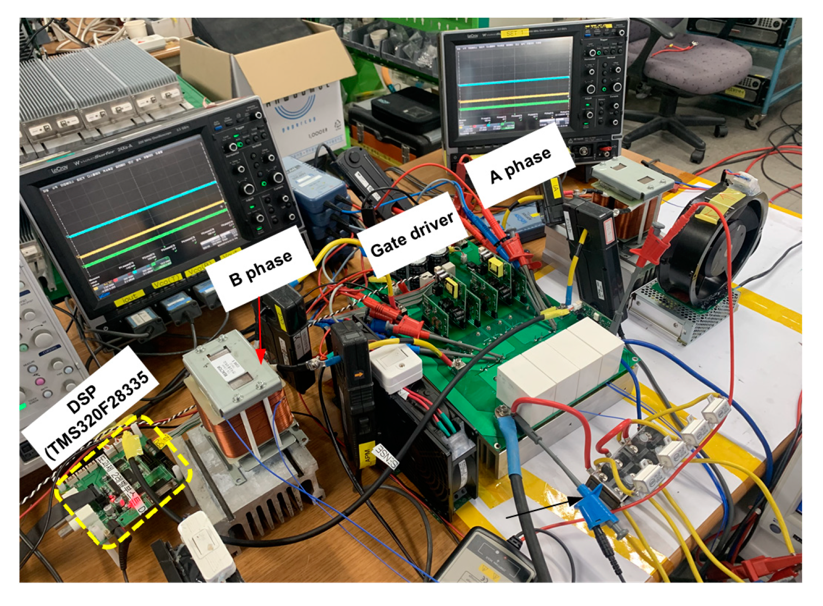
In the controller for the interleaved boost converter, for the balanced inductor current, two parallel current controllers were designed, and its controller bandwidth was set to 100 Hz with 60° phase margin considering 8 kHz sampling frequency. On the other hand, based on the controller for the three-level boost converter, the additional 50 Hz bandwidth with 60° phase margin voltage controller was adopted for the balanced output capacitor voltage and the 500 Hz bandwidth with 60° phase margin single current controller based on 60 kHz sampling frequency was implemented [8,9,10,11,12,13,14]. Figure 16 shows the experimental environment for the prototype hardware.
Figure 17 shows the experimental waveforms of the interleaved boost converter according to the output voltage variations. As shown in Figure 17b,d,f, the inductor currents of the interleaved boost converter are almost equal to each other due to the separated current controller. In addition, the input current ripple of the interleaved boost converter satisfies the current ripple requirement, which is under 10% of the rated current. Furthermore, the output voltage ripples are well constrained under 5 V, which is under 1% of the rated output voltage regardless of the output voltage conditions.
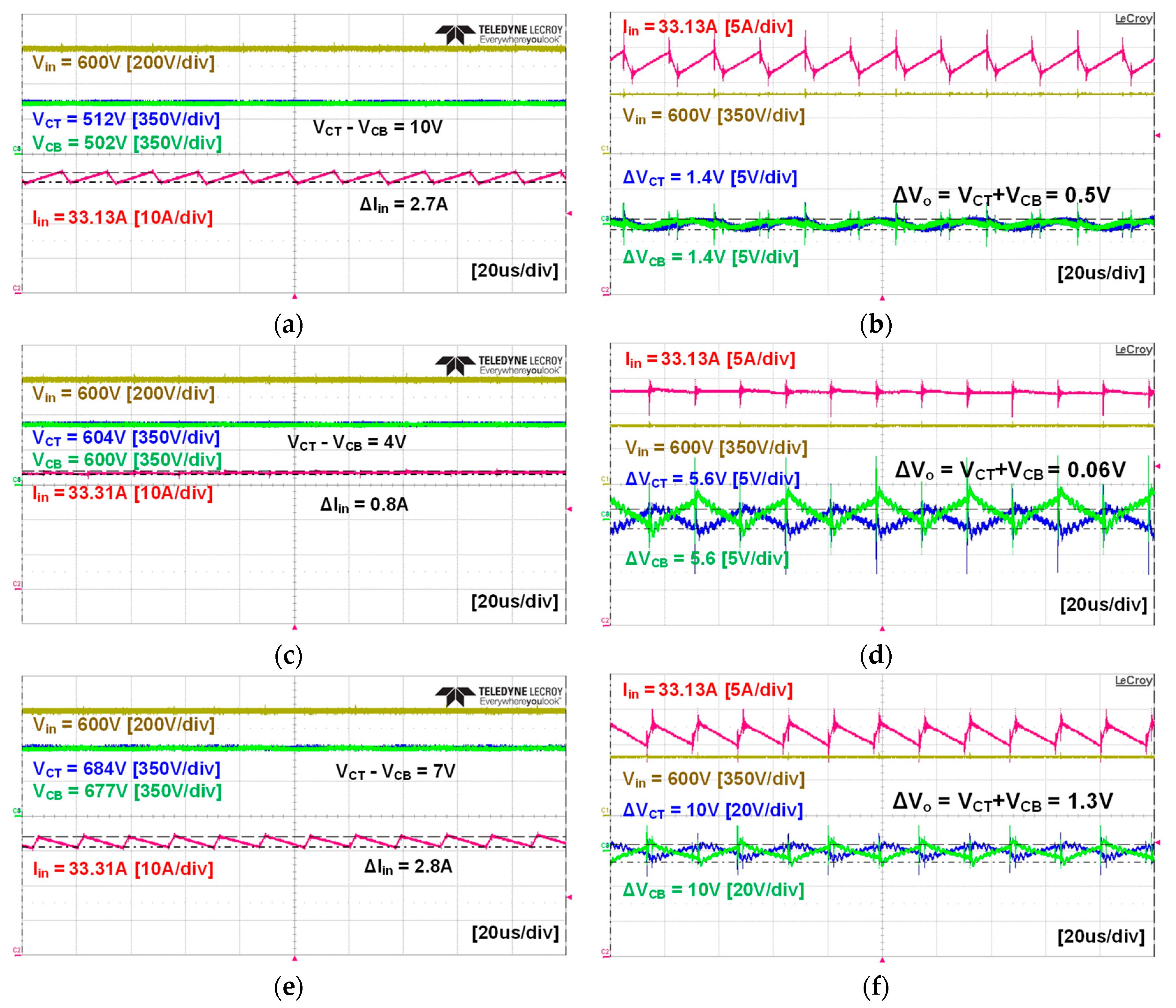
Figure 18 presents the static performance of the three-level boost converter corresponding to the various output voltages. Similar to the interleaved boost converter, the input current ripples of the three-level boost converter maintains under 10% of the rated current even under severe conditions such as high output voltage and full load conditions. In addition, the auxiliary output voltage balancing controller shows satisfactory performance since there is almost zero voltage difference between VCT and VCB. Moreover, the output voltage of the three-level boost converter shows under 10 V voltage ripples, meeting the voltage ripple requirements over the entire output voltage conditions.
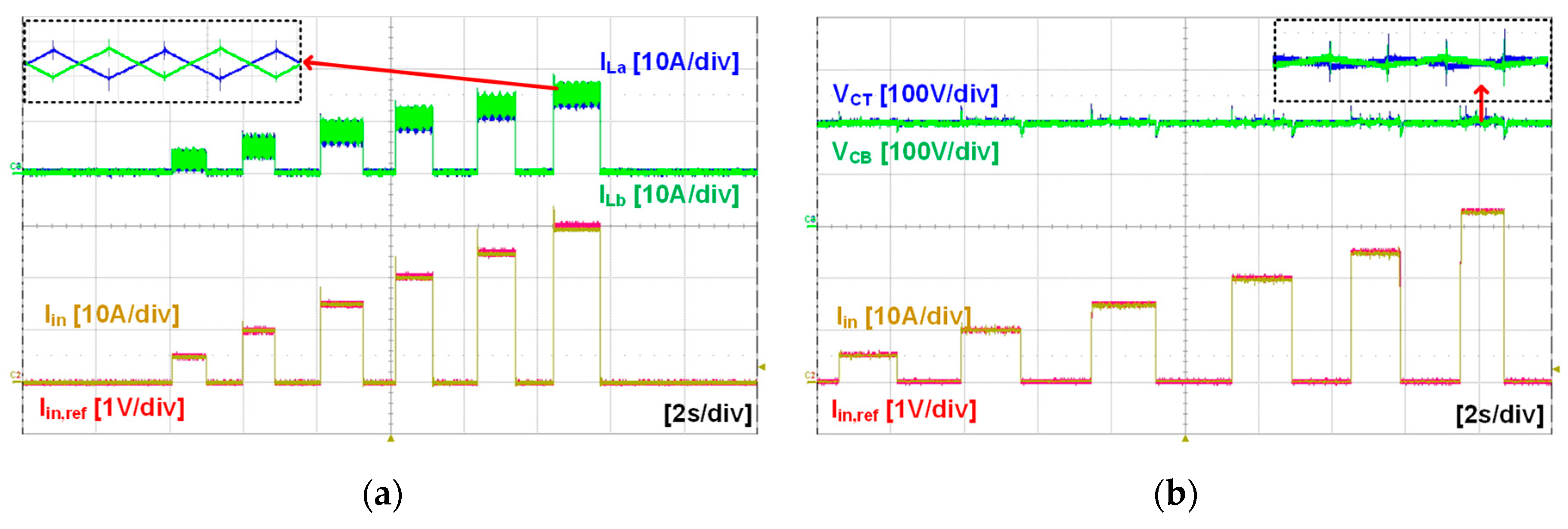
Figure 19 show the dynamic performance of both converters. Due to the restricted experimental equipment environment, such as the limited voltage rating of the electrical load to generate programmed load transient, the dynamin performance experiment is conducted at 200 V input and 400 V output. As depicted in Figure 19, the input currents of both converters precisely not only follow the current reference, but also each current and voltage balancing controls show excellent performance even under 100% load change. As a result, the current and voltage controls for both converters are well designed and adequate for the boost converters for hydrogen-fuel-cell hybrid railway system applications.
Figure 20 and Figure 21 shows the measured power-conversion efficiency according to the various output voltage and load conditions. As shown in Figure 20, both converters show over 97% efficiency at 100% load condition in spite of the output voltage variations. The maximum measured efficiency of the interleaved boost converter is 98.02% in low output and full load conditions. Meanwhile, the maximum measure efficiency of the three-level boost converter is over 99%, and it is 1% larger than that of the interleaved boost converter. This is because the switching and reverse recovery losses of the interleaved boost converter are considerably higher than those of the three-level boost converter, despite the relatively small conduction loss of the interleaved boost converter. In addition, this tendency is deteriorated as the load decreases. As a result, the efficiency of the interleaved boost converter can be lower than 95% in 10% load and high output voltage conditions. On the other hand, because of the low switching loss, the three-level boost converter can achieve more than 96% efficiency irrespective of the load and output voltage conditions. Therefore, through the analysis and experimental results, the three-level boost converter is shown to be more effective for the hydrogen-fuel-cell hybrid railway system than the interleaved boost converter due to the high power density as well as the high efficiency. Figure 21 shows the efficiency measured by a power analyzer at Vin = 600 V, VO = 1360 V, and PO = 20 kW. Its loss breakdown has already been explained in Figure 12. As the calculated efficiency in Figure 12 and measured efficiency in Figure 21 are well matched, it can be said that the loss breakdown is well done.

5. Conclusions

This paper presents and reviews step-up DC/DC converters suitable for high-power density and that are suitably light-weight to apply to the hydrogen-fuel-cell hybrid railway system. By selecting interleaving and three-level boost converters as candidates for step-up DC/DC converters, the operational principle of interleaved and three-level boost converters are described and explained through the analysis and the design considerations for inductor, capacitor and power semiconductor devices is presented based on the theoretical analysis. Moreover, current and voltage balancing controls are adequately designed by utilizing the digital controller, and these can minimize the difference of currents of each phase current in the interleaved boost converter and capacitor voltages in the three-level converter. The validity of the design and analysis for each converter is verified through the experimental results of prototypes with the 600 V input and 1200 V/20 kW output specification since there is only 1% difference between the measured efficiency and expected efficiency through the analysis. In addition, from the experimental results and from comparing the prototype hardware, although both converters are attractive topologies for the high power and step-up DC/DC converter, it is noted that the three-level boost converter is the more promising topology for a hydrogen-fuel-cell hybrid railway system than the interleaved boost converter, due to the high efficiency and high power density.

Author Contributions

I.-O.L. is the main researcher who initiated and organized research reported in the paper and is responsible for designing and anlyzing the system, and writing the paper. H.-S.Y. is responsible for writing and revising the paper. All authors including D.-H.Y. and W.-S.L. are responsible for making the prototype of the proposed system and carrying out the experiment. All authors have read and agreed to the published version of the manuscript.

Funding

This research was funded by “Human Resources Program in Energy Technology” of the Korea Institute of Energy Technology Evaluation and Planning (KETEP), granted financial resource from the Ministry of Trade, Industry & Energy, Republic of Korea. (No. 20174030201790). This research was funded by the National Research Foundation of Korea (NRF) grant funded by the Korea government (MSIT) (2018R1D1A1B07048209).

Conflicts of Interest

The authors declare not conflict of interest.

References

  1. Coradia iLint Hydrogen Train Receives Approval for Commercial Operation in German Railway Networks. Available online: https://www.alstom.com/press-releases-news/2018/7/coradia-ilint-hydrogen-train-recei-ves-approval-for-commercial-operation-in-german-railway-networks (accessed on 6 August 2019).
  2. Lim, S.-M.; Sung, S.-W.; Lee, Y.-K.; Kim, J.W. Technical Trends of Hydrogen Fuel Cell Railway Rolling Stock; The Korean Society For Railway: Jeju, Korea, 2018; pp. 314–317. [Google Scholar]
  3. Meleshin, V.I.; Zhiklenkov, D.V.; Ganshin, A.A. Efficient three-level boost converter for various applications. In Proceedings of the 15th International Power Electronics and Motion Control Conference EPE-PEMC 2012 ECCE Europe, Novi Sad, Serbia, 4–6 September 2012. [Google Scholar]
  4. Yaramasu, V.; Wu, B. Three-Level Boost Converter based Medium Voltage Megawatt PMSG Wind Energy Conversion Systems. In Proceedings of the 2011 IEEE Energy Conversion Congress and Exposition, Phoenix, AZ, USA, 17–22 September 2011; pp. 561–567. [Google Scholar]
  5. Kim, M.K.; Woo, D.G.; Lee, B.K.; Kim, N.J.; Kim, J.S. Loss Analysis of Power Conversion Equipment for Efficiency Improvement. Trans. Korean Inst. Power Electron. 2014, 19, 80–90. [Google Scholar] [CrossRef] [Green Version]
  6. Swamy, H.M.M.; Guruswamy, K.P.; Singh, S.P. Design, Modeling and Analysis of Two Level Interleaved Boost Converter. In Proceedings of the 2013 International Conference on Machine Intelligence Research and Advancement, Katra, India, 21–23 December 2013; pp. 509–514. [Google Scholar]
  7. High Flux Material Curves. Available online: https://www.mag-inc.com/Products/Powder-Cores/High-Flux-Cores/High-Flux-Material-Curves (accessed on 10 October 2019).
  8. Reddy, M.S.; Kalyani, C.; Uthra, M.; Elangovan, D. A Small Signal Analysis of DC-DC Boost Converter. Indian J. Sci. Technol. 2015, 8, 1–6. [Google Scholar] [CrossRef]
  9. Idoia, L.Z. Current Control Design and Implementation for a 2.4 kW Boost Converter for Fuel Cells; Grado en Ingeniería en Tecnologías Industriales: Pamplona, Spain, March 2017. [Google Scholar]
  10. Nouri, A.; Salhi, I.; Elwarraki, E.; el Beid, S.; Essounbouli, N. DSP-based implementation of a self-tuning fuzzy controller for three-level boost converter. Electr. Power Syst. Res. 2017, 146, 286–297. [Google Scholar] [CrossRef]
  11. Khaldi, H.S.; Ammari, A.C. Fractional-order control of three level boost DC/DC converter used in hybrid energy storage system for electric vehicles. In Proceedings of the 2015 6th International Renewable Energy Congress (IREC), Sousse, Tunisia, 21 May 2015. [Google Scholar]
  12. Chen, H.-C.; Lin, W.-J. MPPT and Voltage Balancing Control With Sensing Only Inductor Current for Photovoltaic-Fed, Three-Level, Boost-Type Converters. IEEE Trans. Power Electron. 2014, 29, 29–35. [Google Scholar] [CrossRef]
  13. Yadav, A.; Awasthi, A.; Karthikeyan, V.; Singh, A.K.; Das, V.; Karuppanan, P. Small SIGNAL modeling and stability analysis of N-phase interleaved boost converter. In Proceedings of the 2016 IEEE Uttar Pradesh Section International Conference on Electrical, Computer and Electronics Engineering (UPCON), Varanasi, India, 9–11 December 2016; pp. 585–590. [Google Scholar]
  14. Choudhury, S. Designing a TMS320F280x Based Digitally Controlled DC-DC Switching Power Supply; Application Report SPRAAB3–July 2005; Texas Instruments: Dallas, TX, USA, 2005. [Google Scholar]
Figure 1. Propulsion system for hybrid hydrogen-fuel-cell railway system.
Electronics 09 00771 g001
Figure 2. Conventional boost converter. (a) Circuit diagram. (b) Key waveforms.
Electronics 09 00771 g002
Figure 3. High step-up DC/DC converters. (a) Interleaved boost converter, (b) three-level boost converter.
Electronics 09 00771 g003
Figure 4. Operation key waveforms of the interleaved boost converter according to the duty-ratio. (a) D ≤ 0.5. (b) D > 0.5.
Electronics 09 00771 g004
Figure 5. Topological states of the interleaved boost converter when the duty-ratio is under 0.5. (a) Mode 1 (t0t1). (b) Mode 2 (t1t2).
Electronics 09 00771 g005
Figure 6. Topological states of the interleaved boost converter when the duty-ratio is over 0.5. (a) Mode 1 (t0t1). (b) Mode 2 (t1t2).
Electronics 09 00771 g006
Figure 7. Operation key waveforms of the 3-level boost converter according to the duty-ratio. (a) D ≤ 0.5. (b) D > 0.5.
Electronics 09 00771 g007
Figure 8. Topological states of the 3-level boost converter when the duty-ratio is under 0.5. (a) Mode 1 (t0t1). (b) Mode 2 (t1t2).
Electronics 09 00771 g008
Figure 9. Topological states of the 3-level boost converter when the duty-ratio is over 0.5. (a) Mode 1 (t0t1). (b) Mode 2 (t1t2).
Electronics 09 00771 g009
Figure 10. Voltage-second balance of the interleaved boost converter. (a) D ≤ 0.5. (b) D > 0.5.
Electronics 09 00771 g010
Figure 11. Voltage-second balance of the 3-level boost converter. (a) D ≤ 0.5. (b) D > 0.5.
Electronics 09 00771 g011
Figure 12. Loss comparison of the interleaved and 3-level boost converter at 1360 V/20 kW output. (a) Interleaved. (b) 3-level; Pcore: Inductor’s core loss; Pwire: Inductor’s copper loss; PQrr: Boost diode’s reverse-recovery loss; Pdcond: Boost diode’s conduction loss; PSWcond: Boost switch’s conduction loss; and Pswitching: Boost switch’s switching loss.
Electronics 09 00771 g012
Figure 13. Prototype hardware. (a) Interleaved boost converter: top-view. (b) Interleaved boost converter: side-view. (c) Three-level boost converter: top-view. (d) Three-level boost converter: side-view.
Electronics 09 00771 g013
Figure 14. Inductor’s size. (a) Interleaved boost converter. (b) Three-level boost converter.
Electronics 09 00771 g014
Figure 15. Control block diagram. (a) Interleaved boost converter. (b) Three-level boost converter.
Electronics 09 00771 g015
Figure 16. Experimental environment for the prototype hardware.
Electronics 09 00771 g016
Figure 17. Experimental waveforms of the interleaved boost converter according to 20 kW output with output voltage variations. (a) Vin, VO, and Iin at 1008 V output. (b) Vin, ΔVO, ILa, and ILb at 1008 V output (c) Vin, VO, and Iin at 1200 V output. (d) Vin, ΔVO, ILa, and ILb at 1200 V output. (e) Vin, VO, and Iin at 1360 V output. (f) Vin, ΔVO, ILa, and ILb at 1360 V output.
Electronics 09 00771 g017
Figure 18. Experimental waveforms of the 3-level boost converter according to 20 kW output with output voltage variations. (a) Vin, VCT, VCB, and Iin at 1008 V output. (b) Iin, Vin, ΔVCT, and ΔVCB at 1008 V output (c) Vin, VCT, VCB, and Iin at 1200 V output. (d) Iin, Vin, ΔVCT, and ΔVCB at 1200 V output. (e) Vin, VCT, VCB, and Iin at 1360 V output. (f) Iin, Vin, ΔVCT, and ΔVCB at 1360 V output.
Electronics 09 00771 g018
Figure 19. Experimental waveforms according to load variations at 200 V input and 400 V output. (a) Interleaved boost converter. (b) Three-level boost converter.
Electronics 09 00771 g019
Figure 20. Measured power-conversion efficiency-curves according to the various output voltage and load conditions. (a) Interleaved boost converter. (b) Three-level boost converter.
Electronics 09 00771 g020
Figure 21. Measured power-conversion efficiency at Vin = 600 V, VO = 1360 V, and PO = 20 kW. (a) Interleaved boost converter. (b) Three-level boost converter.
Electronics 09 00771 g021
Table 1. Specifications for prototypes of interleaved and 3-level boost converters.
ParametersValue
Output power (PO)20 kW
Input voltage (Vin)600 V
Output voltage (VO)1200 Vnorm (1008–1360 V)
Output voltage ripple (ΔVO)10.08 V (1% of minimum output voltage)
Input current ripple (ΔIin)3.3 A (10% of maximum input current)
Table 2. Inductor design results of interleaved and 3-level boost converters.
ParametersInterleaved Boost3-Level Boost
Required inductance (Lreq)Lreq = La = Lb = 2.91 mH0.39 mH
Required AP (mm4)
at BM = 0.5 T, Ku = 0.3, J = 6 A/mm2
La + Lb = 1797,014 m4L = 481,385 mm4
CoreLa: High flux 58737, 2EA
(series connected)
Lb: High flux 58737, 2EA
(series connected)
High flux 58737
Core permeability60 μ60 μ
AL,min value of core187.68 nH/T2187.68 nH/T2
Turns for each core/J (A/mm2)112/666/6
Real min inductance (Lmin)
without DC-bias
Lmin = La = Lb = 2.35 mH × 2Lmin = 0.82 mH
Real min inductance (Lmin,dc)
with DC-bias
Lmin,dc = La = Lb = 1.45 mH × 2
at 101 AT/cm
Lmin,dc = 0.39 mH
at 119 AT/cm
Total number of
inductors or cores
41
Table 3. Capacitor design results of interleaved and 3-level boost converters.
ParametersInterleaved Boost3-Level Boost
Required capacitance (Creq)Creq = CO = 15.92 μFCreq = CT = CB = 8.5 μF
Maximum voltage stress1360 V680 V
Capacitor/capacitanceC4AQSBW5220A3NJ × 4EA/
22 μF × 4
CT: C4AQSBW5220A3NJ × 2EA/22 μF × 2
CB: C4AQSBW5220A3NJ × 2EA/22 μF × 2
Number of Capacitor44
Table 4. Switch and diode design results of interleaved and 3-level boost converters.
ParametersInterleaved Boost3-Level Boost
SwitchMax voltage stress1360 V680 V
Max current23.86 A34.86 A
RMS current12.47 A21.3 A
Required margin
(Voltage/Max/
RMS current)
50%/100%/100%50%/100%/100%
Part number
(voltage/drain current)
IXBH25N250
(2500 V/25A at TC = 90 °C)
C3M0032120D
(1700 V/48A at TC = 100 °C)
DiodeMax voltage stress1360 V680 V
Max current23.86 A34.86 A
Average current9.5 A20 A
Required margin
(Voltage/Max/
Average current)
50%/100%/100%50%/100%/100%
Part number
(voltage/average current/VF)
IXBH25N250 (reverse diode),
(2500 V/9.5 A/1.4 V at Tj = 135 °C)
C3M0032120D (reverse diode),
(1700 V/48 A/1.4 Vat Tj = 135 °C)
Table 5. Design results of interleaved and 3-level boost converters.
ParametersInterleaved Boost3-Level Boost
Inductor
(at 100% load)
2.9 mH per phase
(1.45 mH × 2EA,
2-series connection per phase)
Core: Nano crystalline
0.39 mH
Core: Ferrite
CapacitorCO = 15.92 μF
(22 μF × 4EA = 88 μF,
(4-parallel connection)
CT = CT = 8.5 μF
(CT, CB: 22 μF × 2EA = 44 μF,
2-parallel connection per capacitor)
SwitchIXBH25N250 × 8EA
(4-parallel connection per phase)
C3M0032120D× 4EA
(2-parallel connection per switch)
DiodeIXBH25N250 × 4EA
(2-parallel connection per phase)
C3M0032120D× × 8EA,
(4-parallel connection per diode)
Table 6. Key parameters for loss calculation of interleaved and 3-level boost converters.
ParametersInterleaved Boost3-Level Boost
Inductor
(per core)
Rwire100 mΩ30 mΩ
ΔB0.2 T0.018 T
SwitchVCE or Rds_on2.4 V43 mΩ
Coss75 pF129 pF
Ton650 ns22 ns
Toff500 ns19 ns
VF (Body diode)2.4 V2.6 V
Qrr (Body diode)2.97 μC80 nC