1. Introduction
Radio-frequency-identification (RFID) is a widespread technology used to identify and track objects on which small and usually passive tags are installed. Passive and batteryless tags are activated by a continuous wave (CW) radiated by a reader and respond by generating an iso-frequency backscattered field. These operations are simultaneous, as the CW signal is requested to energize the tag while it answers to the reader, but the power levels of the signals generated and received by the reader are quite different by several orders of magnitude. There are few ways to conveniently separate the transmitter and receiver paths, as there are no separated frequency bands for the RF link. Tx and Rx paths can share a single antenna using a circulator or a directional coupler, or two separated antennas can be used for receiving and transmitting. Dealing with real components, the actual isolation can be too low and the CW signal generated by the transmitter can easily jam the receiver. This imposes heavy constraints on the low-noise amplifier stage in terms of dynamic range to avoid its saturation and the desensitization of the receiving channel. Several techniques have been proposed to mitigate this phenomenon that are not limited to the RFID (radio-frequency identification) system, wherein the use of a back-scatter communication exaggerates the effects, and several patents have been issued; for example [
1,
2].
Different approaches have been implemented to try to improve the isolation between the transmitter and the receiver sections in RFID systems [
3,
4], but some key aspects of these approaches are not effective for all applications. As the RF link is full-duplex (the receiver is not blanked while the transmitter is operating), modern RF switches are not usable, and thus fail to a very high isolation degree, but fortunately, RFID has some peculiarities that allow for the relaxation of some relevant figures of merit of the communication link. First of all, as the communication between a tag and a reader is over a short or very short range (few meters), the receiver can tolerate a relatively high amount of noise, up to several tens of dB [
5]). This can be inferred once the receiver sensitivity
, the bandwidth
and the minimum required
(Signal to Noise Ratio) are known. In fact, the receiver noise figure (NF) can be written as:
In UHF RFID systems using Amplitude Shift Keying (ASK) modulation, it can be considered that a reliable communication between a tag and a reader requires a BER , or using ASK modulation, an SNR ≥ 12 dB. The receiver sensitivity and bandwidth of the operating modes that a reader needs to support, known as Listen Before Talk (LBT) and Talk mode, are quite different. Typically, dBm and BW = 200 KHz in LBT mode and dBm and BW = 1.28 MHz in talk mode with corresponding NF ≤ 9 dB and NF ≤ 28 dB in LBT and Talk mode respectively. The solutions proposed in the literature can be divided into two categories:
Analog approaches with the need for custom design of some key elements [
6,
7,
8,
9];
Digital approaches with the need for custom design of active cancellation systems of different complexities [
10] or recurring to custom integrated designs as in [
11].
Analog approaches typically require a customized design of one or more devices of a circuit, as in [
6], where a microstrip directional coupler, used instead of a circulator, has been proposed as the coupling device between the transmitting stage, the antenna and the receiver. This required a microstrip design and optimization in order to achieve high isolation, but at the expenses of degradation of the receiver NF by more than 13 dB. The adoption of a custom directional coupler as the coupling element has been proposed in [
8], wherein it has been demonstrated that, with a proper selection of the reflection coefficient of the isolated port, it is possible to achieve a high degree of isolation, but with a receiver NF of more than 15 dB. Electrically tunable band-pass filters have been proposed in [
9] in order to suppress the transmitter leakage using specialized tunable filters and an integrated downconversion and upconversion circuitry. The proposed solution requires a high degree of customization and the need for an external microcontroller with a NF of the receiver over 9 dB in a 200 kHz channel. Digital approaches, instead, always require the design of a specialized digital system integrated with some key analog devices. A canceller circuit of this kind has been proposed in [
10], wherein a cancellation loop was designed with a voltage variable attenuator and phase shifters that are controlled by a microprocessor in order to inject an out of phase replica of the unwanted signal coming from the transmitter into the receiver. The adaptive cancellation has allowed a typical isolation of around 30 dB with a good receiver NF less than 1 dB. A deeply integrated solution has been proposed in [
11] with a small, fully specialized CMOS chip able to reach a carrier suppression of around 55 dB with a receiver NF of more than 18 dB. Regardless of the approaches used in these anti-self-jam solutions, it is important to remember that while the main goal is to achieve high isolation between the transmitter and the receiver, it is equally important to minimize the insertion loss between the antenna and the receiver. The overall self-induced jamming cancellation performance of an anti-self-jam circuit depends on the ratio between two signals entering the receiver: the signal coming from the antenna and the interfering signal coming from the transmitter. The purpose of this work is to propose a novel, fully-analog, self-jamming canceller using only SMT, low-cost, off-the-shelf devices and verify its feasibility using an innovative modular microwave by X-Microwave, without resorting to custom design.
2. Materials and Methods
A generic analog self-jam canceller is reported in
Figure 1 where a transmitter and receiver share the same input/output ports using hybrid couplers as isolating combiners. If all the devices are ideal, the TX/RX isolation is theoretically infinite; if a transmitter injects a signal
into the circuit at port 1, the corresponding output signal can be written as:
where
is the corresponding scattering parameter of the circulators, supposed to be equal, and
are the corresponding scattering parameters of the hybrid couplers.
A signal from port 2,
, is transferred to port 3 (receiver port) as:
The theoretical signal arising from port 1 to port 3 is:
Resulting in nearly perfect isolation and a very low path loss from port 1 to port 2, as indicated in
Figure 2.
Some strong assumptions have been made in the previous analysis; the two circulators are assumed to be identical, and the same is true for the three hybrid couplers. Moreover, the couplers have been considered to be perfectly matched with infinite isolation between ports 1
h, 2
h and 3
h, 4
h. Using actual devices, the situation changes significantly. A finite isolation between the input ports of the hybrid couplers, usually worse than the reverse isolation of a generic circulator operating in the same band, creates two spurious paths that causes the isolation between the transmitter and receiver ports of the circuit vanish. In fact, neglecting reflections, it is possible to write:
thus, the isolation can be:
so
As a hybrid coupler is a passive and reciprocal device,
, Equation (
7) can be rewritten as:
If the isolation of the circulators can be assumed to be high enough, the dominant contribution to
is due to the isolation of the hybrid coupler connected to port 2 of the schematic. It is to be remarked, however, that Equation (
8) does not take into account reflections that still exist. Replacing the ideal hybrid couplers with actual devices, specifically, Mini-Circuits
, the performance degrades, as shown in
Figure 3.
The cancellation is quite similar to the isolation parameter of the hybrid coupler reported in
Figure 4.
Proposed Solution
The topology of
Figure 1 can be conveniently modified in order to try to overcome the intrinsic limitation due to the nature of the actual devices. Looking at
Figure 5, the transmitted signal injected into port 1 is split in two separated and specular branches out of phase. For the first one, in the the upper part of the diagram, one can see the signal traveling through a circulator and toward port
of a hybrid combiner. The signal coming from the lower branch reaches port
of the same hybrid combiner. The signals that are 180 degrees out of phase are combined by an additional 90 degree phase shift. These signals are ready to be used for powering, as an example, a sequentially rotated patch array in order to generate a circular polarized beam without the need for an external 180 degree hybrid. The signal injected in port 1 that is split in two anti-phase branches reaches the port 3s of the circulators and is summed. The spurious paths from port 1 of the circuit to port 3 of the zero degree power combiner, passing through port
and
(as well from port
and
) of the 90 degree output hybrid combiner cancel each other at port 3 (RX) of the circuit. Signals coming from port 2 and 4 of the circuit are combined through the hybrid combiner and summed at port 3 of the circuit through the zero-degree power combiner.
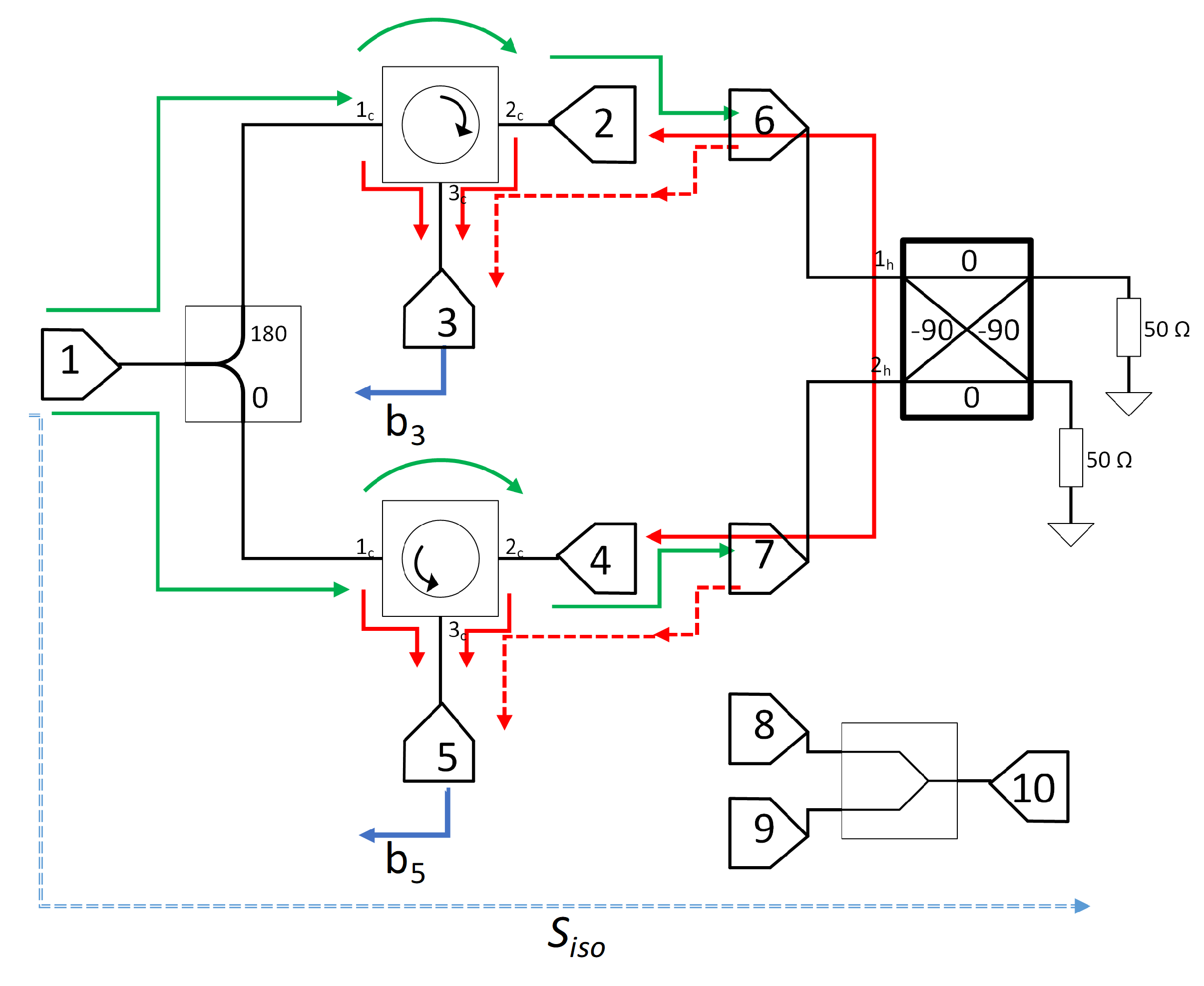
The circuit can be analyzed in detail by splitting it into three main parts: the input network made by the 180 degree splitter and the circulators, the 90 degree hybrid combiner and the zero degree combiner on the receiving path. With reference to the circuit schematic in
Figure 6, green, red and dashed red arrows represent, respectively, direct, undesired and reflected signals. Considering the hybrid combiner terminated in matched loads, the transmitted wave
on the upper path can be written as:
The transmitted wave
on the lower path can be written as:
The output signal, that is, the isolation contribution,
can be described as:
Some considerations can be made: The hybrid combiner is a passive and reciprocal network, so
while it can be assumed that
and
, with
and
as the scattering parameters of the forward path of the circulators (
of the devices) and the path from port 1 to port 2 of the circuit of
Figure 6 respectively. Equation (
9) can be written as:
and Equation (
10) as:
If
than:
For the zero degree combiner it can be assumed that
so that the isolation can be written as:
Equation (
15) suggests that if
and
, then the isolation could be infinite, but there are also other favorable combinations, as in actual devices the
parameters can be of the same order of magnitude as the circulators isolation obtaining
. Isolation is theoretically granted even if ports 1 and 4 of the hybrid coupler are terminated with equal but mismatched loads. In this case the contributions due to the reflected waves from the transmitter are summed out of phase at the receiver power combiner.
3. Simulated and Experimental Results
The circuit has been simulated with NI-AWR Microwave Office (MWO) [
12] using the measured and available scattering parameters of the selected devices:
Mini-Circuits Balun;
Skyworks MAFR000688 Circulators;
Mini-Circuits ADP-2-10 in-phase Power Combiner;
Mini-Circuits QCN-12A 90 degree Hybrid Combiner.
The proposed solution has been translated in a MWO schematic where all the ideal devices have been replaced with the corresponding real devices, as shown in
Figure 7.
The simulated performance of the circuit is reported in
Figure 8 where the isolation from transmitting and receiving ports is well over 30 dB from 860 MHz to 960 MHz. The insertion losses from ports 2 and 4 to port 3, the receiver, are quite similar to the insertion losses from port 1 to ports 2 and 4, at around 4.5 dB.
Moreover, results predicted by Equation (
15) are reported in
Figure 9 together with those coming from the simulation of the circuit, and are very close to each other within an error of 0.2 dB.
The scheme has been realized using an innovative rapid prototyping and modular technique by X-Microwave [
13]. The circuit has been sectioned into small drop-in components called X-MWblocks, and each one is devoted to a specific task, as clearly shown in
Figure 10.
The proposed technique allows rapid and reliable prototyping and the opportunity to re-configure the hardware without having to redesign each time. Each drop-in has been realized with a 49 mil 4-layer stackup PCB using 8 mil Rogers RO4003 substrate as the top RF Core. The input port of the circuit, port 1, is probed with a high performance 2.92 mm connectorized microwave probe (X-MWprobe). The RF probe is connected to a
Balun populated on a dedicated 0409 format PCB (i.e., 4 × 9 grid spaces), using CPWG (coplanar waveguide with lower ground plane) microstrip transmission lines. The Skyworks MAFR000688 circulators have been integrated on two 1009 format PCBs and the connections with the
have been made by two 50 Ohm “S” shaped transmission lines. Port 2 of each of the circulators has been connected to the cascade of a couple of small Mini-Circuits RCAT-XX attenuators and transmission lines in order to complete the RF paths, and to be easily replaced with other components, as necessary. Two auxiliary 0409 format “S” shaped transmission lines, close the electrical paths from the transmitter port to the QCN-12A 90 degree hybrid combiner, were integrated on a dedicated 0409 format board. The output ports of the hybrid combiner are connected to two more high performance 2.92 mm X-MWprobes. Port 3 s of the two circulators are connected to the PCB with the Mini-Circuits ADP-2-10 in-phase power combiner on board through two phase-matched hand formable coaxial cables. All of the solderless interconnections between the boards are formed by special ground-signal-ground jumpers (gsg jumpers), which are small pieces of polyimide material with copper traces that are shaped to maintain 50 ohm impedance while bridging the 5 mil air gap from launch to launch of adjacent blocks. The copper traces of the gsg are coated with diamond particles and then gold-plated, creating high performance diamond particle interconnections. The gsg jumpers are then laid across each port of two boards, and two anchors are used to hold them firmly against the PCB on each side of the connection, as is clearly visible in
Figure 11.
Every microstrip PCB is screwed to a metal prototype plate using dedicated screws in order to obtain a mechanically robust assembly while assuring a very good ground path to all the devices. The complete circuit shown in
Figure 10 was assembled with one hex driver (no solder or epoxy required). The circuit has been characterized using a Keysight PNA-X N5247B 67 GHz Vector Network Analyzer [
14] by extracting the 4-port matrix of the circuit, as is visible in
Figure 12.
The simulated input matching and measured input matching of the 4-port circuit are reported in
Figure 13.
The simulated and measured insertion losses of the transmitting paths are reported in
Figure 14, where the differences between the theoretical and actual values are within 1 dB.
The isolation between the input port (transmission) and the receiver port is visible in
Figure 15. The experimental data concerning the isolation parameter are slightly better than the simulated data by 1.5 dB.
The carrier over jammer suppression can be defined as:
with
C and
J as the signal available at port
3 (receiver) coming from ports
2 and
4 of
Figure 7, and the unwanted component from port
1 (transmitter) to port
3 (receiver) respectively. It is clear that, in this case, the transmitter behaves like a jammer for the receiver. The
(C/J) behavior of the scheme is reported in
Figure 16 where the actual performance is slightly better than the simulated performance—within 0.5 dB to 3 dB over the entire bandwidth with an average suppression better than 36 dB all over the bandwidth.
4. Discussion
In this paper, a novel, low-cost, fully-analog anti-self-jam circuit suitable for UHF RFID has been presented. The theory has been developed and the subsequent validation has been carried out using the innovative modular technology made available by X-Microwave through which it was possible to create a prototype and verify its performance in a very short time, while obtaining even better results than those expected from the simulations. The aim of the solution has been to try to simplify the hardware as much as possible, by minimizing the required components and using compact and low-cost SMT devices. The estimated cost of all the required components is less than 30 € for very small quantities, granting further huge potential savings for typical production volumes for a circuital solution designed for a RFID reader and not for a very low-cost device like a tag. The proposed scheme demonstrated very good anti-self-jam performance with a measured (C/J) better that 36 dB and a NF ≤5 dB over the entire bandwidth. The next step is to optimize the circuit, to achieve even greater margins, and to achieve a compact, high performance circuit.

