Article

A Reconfigurable Analog Baseband Circuitry for LFMCW RADAR Receivers in 130-nm SiGe BiCMOS Process

1
Institute of Microelectronics, Chinese Academy of Sciences, Beijing 100029, China
2
Institute of Microelectronics, University of Chinese Academy of Sciences, Beijing 100049, China
3
Institute of Electronic Engineering, China Academy of Engineering Physics, Mianyang 621054, China
4
Microsystem & Terahertz Research Center, China Academy of Engineering Physics, Mianyang 621054, China
*
Author to whom correspondence should be addressed.
Electronics 2020, 9(5), 831; https://doi.org/10.3390/electronics9050831
Submission received: 21 April 2020 / Revised: 6 May 2020 / Accepted: 15 May 2020 / Published: 18 May 2020
(This article belongs to the Section Microelectronics)

Abstract

:
A highly reconfigurable open-loop analog baseband circuitry with programmable gain, bandwidth and filter order are proposed for integrated linear frequency modulated continuous wave (LFMCW) radar receivers in this paper. This analog baseband chain allocates noise, gain and channel selection specifications to different stages, for the sake of noise and linearity tradeoffs, by introducing a multi-stage open-loop cascaded amplifier/filter topology. The topology includes a course gain tuning pre-amplifier, a folded Gilbert variable gain amplifier (VGA) with a symmetrical dB-linear voltage generator and a 10-bit R-2R DAC for fine gain tuning, a level shifter, a programmable Gm-C low pass filter, a DC offset cancellation circuit, two fixed gain amplifiers with bandwidth extension and a novel buffer amplifier with active peaking for testing purposes. The noise figure is reduced with the help of a low noise pre-amplifier stage, while the linearity is enhanced with a power-efficient buffer and a novel high linearity Gm-C filter. Specifically, the Gm-C filter improves its linearity specification with no increase in power consumption, thanks to an alteration of the trans-conductor/capacitor connection style, instead of pursuing high linearity but power-hungry class-AB trans-conductors. In addition, the logarithmic bandwidth tuning technique is adopted for capacitor array size minimization. The linear-in-dB and DAC gain control topology facilitates the analog baseband gain tuning accuracy and stability, which also provides an efficient access to digital baseband automatic gain control. The analog baseband chip is fabricated using 130-nm SiGe BiCMOS technology. With a power consumption of 5.9~8.8 mW, the implemented circuit achieves a tunable gain range of −30~27 dB (DAC linear gain step guaranteed), a programmable −3 dB bandwidth of 18/19/20/21/22/23/24/25 MHz, a filter order of 3/6 and a gain resolution of better than 0.07 dB.

1. Introduction

The booming smart portable devices has led to an imperative demand for multi-standard compatibility on mobile/wireless receivers in recent years, such as Global System for Mobile Communications (GSM), Bluetooth, Global Position System (GPS), Wideband Code Division Multiple Access (W-CDMA), Wireless Local Area Network (WLAN), Long Term Evolution (LTE), and so on. Therefore, industrial corporations and academic institutions have released diverse integrated solutions with different RF front-ends covering various bands and sharing one analog baseband, which performs channel selectivity and gains tunability functions after down conversion mixers. In general, the analog baseband should be optimized for multi-purpose application scenarios with a fundamental tradeoff between noise figure, linearity, power consumption, channel selection and gain/bandwidth/filter order programmability in itself. The fundamental principle, which prevents the analog baseband from obtaining universality, is that: the noise figure is determined by the preceding stages while the linearity is decided by the backward ones. The major challenges to be settled in the design of flexible analog circuits are the following: a. performance programmability; b. specification compatibility; c. energy scalability; d. complexity and cost.
In direct conversion receivers, typical analog baseband consists of a programmable gain amplifier (PGA) and a low-pass filter (LPF) as depicted in Figure 1. Thus, two general architectures emerge with their respective pros and cons: the LPF-first topology is more suitable for the receivers with high linearity/medium noise figure, while the PGA-first topology fits the receivers more with low noise figure/medium linearity. The authors of [1] proposed a fourth-order Chebyshev active-R-C LPF + PGA + fourth-order Chebyshev active-R-C LPF topology, which emphasized the filtering capability. The authors of [2] proposed a third-order LPF + PGA topology. The authors of [3] proposed a discrete time IIR LPF + active FIR topology, which focuses on the discrete time filtering function. The authors of [4,5,6,7,8] proposed a typical LPF + VGA topology, with tunable cut-off frequency/noise/gain performances. The authors of [9] proposed a fourth-order merged closed-loop analog baseband topology, which integrates the channel selection and gain programmability in one merged PGA/LPF biquad. However, the closed-loop topology is intrinsically power-hungry and frequency limited since the operational amplifier should exhibit gain bandwidth product (GBW) several times larger than closed-loop bandwidth requirement [10,11]. Therefore, there is no unique optimum solution, but a myriad solution with a variety proportional to the number of input specifications, with the expectation of sufficiently fine gain resolution, bandwidth programmability, excellent noise/linearity performance, acceptable chip footprint and low power consumption.
In this paper, a highly reconfigurable open-loop analog baseband prototype chip is proposed with optimized noise/linearity/power consumption performance, and digitally programmable bandwidth/gain/filter order for integrated linear FMCW radar receivers. Power consumption minimization is achieved via two methods: a. open-loop analog baseband chain with feasible compensations for process/voltage/temperature (PVT) variations; b. allocating channel selection/signal amplification specifications to every block across the baseband chain, and adjusting current consumed for diverse gain levels. The noise figure is maintained low with the help of a low noise figure/high gain pre-amplifier, while the linearity of the Gm-C LPF is guaranteed with a novel connection style without any rise in power consumption. Moreover, a novel high linearity buffer amplifier with active peaking is designed for testing purposes. The proposed prototype is fabricated in a 130 nm SiGe BiCMOS process, and the experimental results demonstrate the practicality of the proposal.
The rest of the paper is organized as follows. After the introduction given in Section 1, Section 2 derives the LFMCW radar requirement on the overall analog baseband chain, Section 3 illustrates the detailed implementation schematic, Section 4 demonstrates the experimental results and Section 5 concludes the paper.

2. Analog Baseband Architecture for LFMCW Radar

LFMCW radars are expansively used in automotive anti-collision, security check, imaging and presence detection applications when high range resolution is required in localization/tracking. A variety of modulation schemes are available, with a transmitted frequency signal acting as sine wave, sawtooth wave, triangular wave or square wave. In a sawtooth wave-based FMCW radar, the achievable range and velocity resolution depend on the transmitting signal bandwidth BW and the linear chirp period Tm, as seen in Figure 2. The range resolution Δr, which refers to the minimum detectable separation distance of two targets of equal cross sections that can be differentiated as distinct targets, is proportional to c/2/BW, where c is the velocity of light. This means that a large modulation bandwidth BW is needed for a fine range resolution. For a transceiver operating at 94 GHz, a modulation period in the order of 100 µs, a modulation bandwidth of higher than 500 MHz, the analog baseband bandwidth can be calculated as follows:
K = B W T m
f d o p p l e r 2 · v c · f o
f I F , s t a t i c = 2 · K · r c
f I F , m o v i n g = 2 · K · r c + f d o p p l e r
where BW is the transmitting signal bandwidth, Tm is the linear chirp period, K is the FMCW slope, fo is the center operating frequency, v is the target velocity, c is the velocity of light, r is the distance from source to target, fIF,static is the analog baseband frequency for static target ranging, and fIF,moving is the analog baseband frequency for moving target ranging. After setting BW = 500 MHz, Tm = 100 µs, c = 3 × 10⁸ m/s, r = 6~7 km into Equations (1)–(4), we can calculate the fIF,static to be 20~23.4 MHz. When doppler radar effect is taken into account, the IF frequency should cover the range of 18~25 MHz. Therefore, for generally used LPFs, the analog baseband −3 dB bandwidth is set to be 18/19/20/21/22/23/24/25 MHz, with 3-bit digital control words to cover the frequency shift coming from potential target moving.
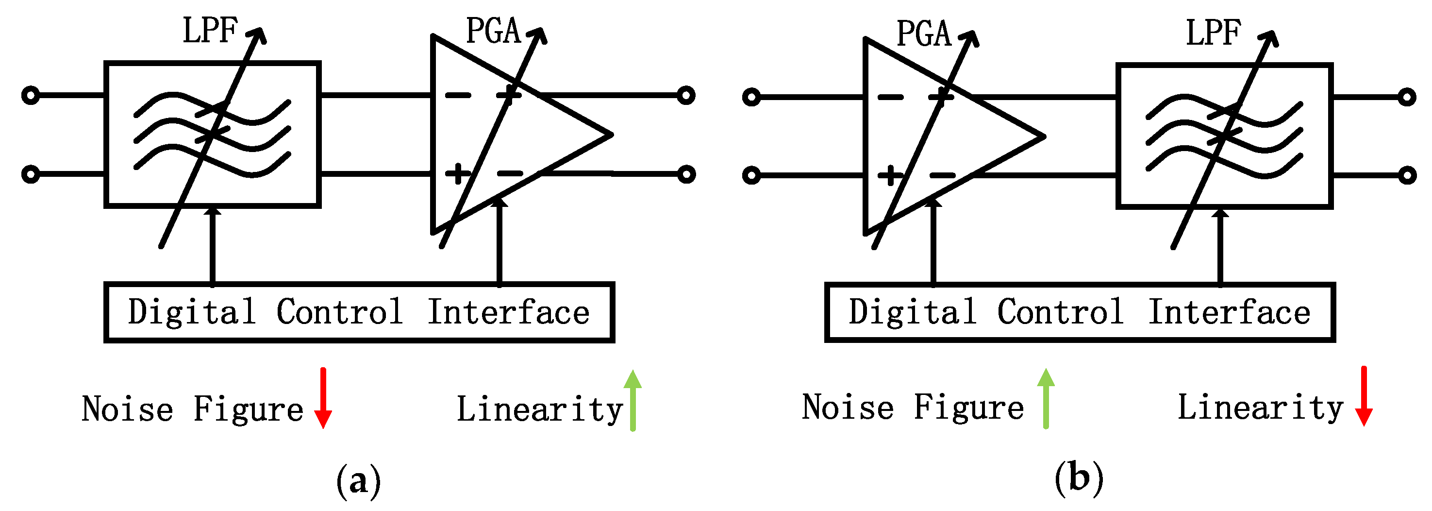
In this LFMCW radar, direct conversion architecture is adopted to evade image rejection problems and, thus, the analog baseband consumes lower power, since its bandwidth is half of that in low-IF/super heterodyne receivers. Paradoxically, typical dynamic range of direct conversion receiver is lower than that of low-IF/super heterodyne ones. Therefore, novel dynamic range optimization techniques are investigated in two directions: lower noise figure and higher linearity. Merged PGA/LPF biquads in [9] simultaneously optimized the two specifications owing to a closed-loop topology with switchable filter orders. However, this kind of topology becomes power-hungry when the frequency rises, and its gain resolution depends on the resistor/capacitor array size. In other words, the merged analog baseband compromises power consumption and chip size for noise/linearity/gain/filter order reconfigurability. What is more, the noise figure of PGA/LPF is normally higher than 25 dB, which deteriorates the receiver noise specification, since the front-end (including a low noise amplifier and a mixer) of the linear FMCW receiver usually possesses a gain of lower than 20 dB. Thus, architectures in Figure 1 and the merged analog baseband in [9] cannot satisfy the noise/linearity/power consumption requirement concurrently.
This paper makes a modification to the LPF-first/PGA-first topology by adding a programmable gain pre-amplifier with course gain tuning ability to its front, as depicted in Figure 3, which forms a PGA-LPF-PGA topology. In detail, this topology includes a pre-amplifier for noise optimization and course gain tuning, a folded Gilbert variable gain amplifier (VGA) with a symmetrical exponential voltage generator and a 10-bit R-2R DAC for fine gain tuning, a level shifter, a programmable Gm-C LPF, a DC offset cancellation (DCOC) circuit, two fixed gain amplifiers (FGA) with bandwidth extension and a novel buffer amplifier with active peaking for testing purposes. DC coupling is utilized on account of spectrally efficient modulation schemes [12]. The architecture in Figure 3 is open-loop and thus, frequency/power scalable. From the LPF-first viewpoint, this topology optimizes noise figure with another PGA ahead. From the PGA-first viewpoint, this topology ameliorates linearity with another PGA behind. Nonetheless, a heavy signal-processing burden is placed upon the LPF and its high linearity is a prerequisite.
In search of a high linearity LPF, researchers proposed numerous high linearity structures, such as active-R-C and class-AB Gm-C ones [6,13,14,15,16]. Linearity is refined with a compromise of power consumption and operation frequency, which is fundamentally determined by the closed-loop LPF topology and the complex routings inside the trans-conductor. Thus, high linearity open loop LPFs, which theoretically decouples the linearity from power consumption, are urgently needed.

3. Detailed Circuit Designs

In this section, detailed sub-block circuit schematics and their respective design procedures are presented.

3.1. Pre-Amplifier

As the first stage in the analog baseband chain, the pre-amplifier should exhibit low noise figure and simultaneously sufficient gain to suppress the noise contribution from the following stages to the overall analog baseband circuitry. Moreover, the gain programmability serves as a critical safeguard for large variations in input signal strength and a powerful certification of automatic gain control (AGC). Class-A/AB amplifiers are usually selected with common mode stability circuitry, with a high noise figure attributed to circuit complexities. Although the three fundamental gain programmability schemes, including current switching/bleeding, load resistor switching and source degeneration, are reported as depicted in Figure 4, their merits and demerits are evident: a. current switching method dynamically varies gain by correspondingly adjusting biasing current. High gain typically corresponds to high linearity/low noise figure/high dynamic range, while low gain is in accordance with low linearity/high noise figure/low dynamic range. Therefore, the dynamic range fluctuates over all gain settings; b. load resistor switching assumes a gain switching scheme with little noise figure variations, since the noise contribution from load resistors is restrained by amplifying the transistors. However, the load resistor switching has a detrimental effect on voltage swings and thus, the voltage swing varies with gain; c. the source degeneration scheme monitors the transconductance of main amplification transistors with a corresponding adjustment in noise figure and linearity. When the gain is high, a weak source degeneration is formed with a low noise figure and a medium linearity. When the gain is low, a strong source degeneration is constructed with a high linearity and a medium noise figure. Nevertheless, the current consumption is stable over all gain settings, which deteriorates the power dissipation self-adaptability. The advantages and disadvantages of them are listed in Table 1.
Forasmuch as the low noise and course gain tuning requirements, this paper utilizes a limiting amplifier structure with no common mode control [12] and adds 3-bit gain programmability with a switched resistor source degeneration technique, which is depicted in Figure 5. The common mode stabilization is left to following stages with noise figure optimization. Although the issue of stable current consumption still exists as one in source degeneration structure, the limiting amplifier structure avoids the common mode control circuitry, which is usually power-hungry. In short, the power consumption problem is partially circumvented. The component sizes and post-simulated specifications at TT 27° are given in Table 2.

3.2. VGA and Symmetrical Exponential Voltage Generator

Intrinsically, Gilbert structure can be regarded as a hybrid combination of current switching and load resistor switching since the current is simultaneously split between load resistors R1/R2 and tail currents Itail1/Itail2 in Figure 6. Therefore, an optimization regarding the pros and cons of the two schemes can be conducted for the sake of dynamic range expansion. In essence, the Gilbert cell adjusts its gain via the current switching technique, but the difference between current switching and Gilbert cell lies in the current feeding through load resistors. In the Gilbert cell, the current through load resistors is stable across all gain settings, which circumvents dynamic range fluctuations encountered in current switching technique. Thus, the Gilbert structure is utilized for its wide gain tuning range and robustness, while a dB-linear voltage generator with an R-2R DAC is utilized for digital gain tuning precision. The variable gain amplifier cell with its control voltage generator is depicted in Figure 6. Moreover, dual supply voltages 1.2 V/1.8 V are adopted for power optimization. Specifically, 1.8 V feeds VGA, while 1.2 V feeds the voltage exponential generator.
In the VGA cell, assuming the transistors are working in strong saturation regions and square law model is adopted, the linear relationship between the input and output of VGA is expressed as follows:
V o u t = ( g m 1 , 2 g m 3 , 4 ) · R 1 , 2 · ( V i n p V i n n )    = μ n C o x ( W L ) 1 , 2 , 3 , 4 2 I t a i l · g m 5 , 6 · R 1 , 2 · 2 · R 3 , 4    · I s a t u r a t i o n · exp ( V c t r l V T ) · ( V i n p V i n n )
where µn is the low field mobility coefficient, Cox is the unit area oxide capacitance and W/L is the aspect ratio of the transistors. The voltage gain is in a dB-linear relationship with the input voltage as expressed in Equation (5). The component sizes and post-simulated specifications at TT 27° are given in Table 3.

3.3. DAC

R-2R DAC is employed to facilitate the digital control of the dB-linear voltage generator and to ensure fine gain resolution, with a single pole double throw (SPDT) based gain tuning scheme, switchable between analog continuous tuning and digital step tuning [8]. A 10-bit R-2R DAC with its output buffer is depicted in Figure 7. Two respective voltage ports named Vrefh and Vrefl refer to the high and low reference voltages, which are in accordance with Figure 3. The unit resistor value is selected to be 14.95 Kohms, with accuracy in mind.
In the design of a 10-bit DAC, component accuracy, symmetry of differential components and environmental consistency are three crucial points in layout floor planning. Thus, dummy cells near key components, shielded signal path optimization should be iterated several times. In addition, the output buffer should possess rail to rail output swing and acceptable drive capability. Therefore, the folded cascode topology depicted in Figure 7b is chosen with a linearization technique.
In the static simulation of the whole DAC, the full voltage range is 1.2 V, the INL is 0.17 LSB and the DNL is 0.34 LSB. In dynamic simulations, a sampling frequency of 1 MHz, with a sinusoidal input signal of 0.4961 MHz, is chosen and the effective number of bits (ENOB) is higher than 9.88 bits.
The component sizes and post-simulated specifications at TT 27° are given in Table 4.

3.4. Level Shifter

In between VGA and LPF, a level shifter is inserted for the sake of common mode voltage stabilization, since its preceding pre-amplifier and VGA do not provide this kind of function. The level shifter is depicted in Figure 8, and a typical one-stage amplification with two-stage DC voltage feedback is used. R2/C1 performs the gain/phase margin compensation and snake resistors layout are utilized with large MOS-capacitors. The component sizes and post-simulated specifications at TT 27° are given in Table 5.

3.5. Programmable Gm-C LPF

Gm-C filters are well known for their open loop and frequency scalable characteristics. In theory, the Gm-C topology with simplicity, modularity and programmability would be the perfect choice for high frequency continuous-time filter designs. However, the mediocre linearity specification limits its potential use in analog baseband chain of direct conversion receivers. Therefore, linearity improvement techniques are pursued in two aspects: a. the transconductor cell [5,6,7,8]; b. the filter architecture. Most relevant work focuses on the former one with an emphasis on class AB transconductors. Nonetheless, class-AB transconductors are inherently power-hungry and possess a medium noise figure [10]. In addition, its common mode feedforward and feedback circuitry needs special care in common mode analysis, and its layout and routing are complex [6,13]. Moreover, previously reported linearity enhancement techniques in class-A transconductors are categorized into five groups: a. source degeneration; b. cross coupled transistors; c. load switching; d. current bleeding; e. local gm-boosting feedback. None of them offers an architectural approach to promote linearity. This paper proposes a modified 3rd order Butterworth LPF with 3-bit logarithmic bandwidth tuning ability, as depicted in Figure 9.
Traditional third-order Butterworth LPF is depicted in Figure 9a, with a bandwidth tuning technique. From the bi-quad cascading viewpoint, an exchange of V2+ and V1− is conducted as in Figure 9b. The voltage-current relationships of the two bi-quads are derived as follows.
I c , l e f t = g m · ( V 1 + V 2 + ) + g m · ( V 2 V 1 )   = g m · ( V 1 + + V 2 V 1 V 2 + )
I c , r i g h t = g m · ( V 1 + V 1 ) + g m · ( V 2 V 2 + )    = g m · ( V 1 + + V 2 V 1 V 2 + )
Therefore, the output current remains the same for the two bi-quads. A quick glimpse of the right half of Figure 9b reveals that for a typical transconductor cell (Gm in Figure 9), the differential input signal swing is replaced by common mode input signal swing. Since the major nonlinearity is attributed to the transconductor itself, this change circumvents the differential signal processing vulnerability, with a new burden on common mode signal processing ability. On one hand, differential input signals experience the same voltage-to-current transformation in transconductor cells. Therefore, the frequency response remains the same after the modifications. On the other hand, common mode input signals experience different path, which results in larger variations in common mode signal swing. In short, the modification method essentially linearizes the LPF with an increase in common mode voltage variation, and a corresponding reduction in the differential mode voltage swing in the meantime. Therefore, the common mode rejection ratio and common mode feedback circuit should be designed iteratively with an emphasis on common mode stability. It should be cautious to use traditional sharing technique of common mode feedback circuit.
Afterwards, similar input exchange procedures are executed in Figure 9a and, thus, Figure 9c demonstrates the modified Gm-C LPF with its individual transconductor cell and switched capacitor array. Simulation results show that the output third-order interception point (OIP3) of a third-order Butterworth LPF is elevated from around 4.5 dBm to 14.5 dBm.
As to the bandwidth tuning aspect, typical binary capacitor array cannot set the bandwidth linearly when the operation frequency range covers several decades. For typical LPF, the −3 dB bandwidth is determined as follows.
f o = 1 2 π L C
where fo is the −3 dB cutoff frequency, L is the inductance value and C is the capacitance value. Thus, C is in a square root relation with fo. For example, in order to achieve 2% step size in bandwidth over two decades of the frequency range, a 6-bit resolution in bandwidth programmability is required (26 > 1/2%), while higher than 12-bit resolution is a prerequisite in capacitor array (1002/982 requires another resolution of 6-bit for the lower than 0.025 capacitance resolution), which wastes the majority of the chip area. Therefore, the logarithmic bandwidth tuning technique is also adopted in the LPF design, as depicted in Figure 9c, since the logarithmic equation shrinks the capacitor array into small scale. The individual capacitor value can be calculated with a Taylor series expansion method, as follows:
C 3 b i t , t o t a l = C u n i t · 2 4 b 2 + 2 b 1 + b 0 2    = C u n i t · [ 1 + log 10 ( 2 · 4 · b 2 + 2 · b 1 + b 0 2 ) + 1 2 · ( log 10 ( 2 · 4 · b 2 + 2 · b 1 + b 0 2 ) ) 2 ] +    = C u n i t · [ 1 + ( 2 1 ) b 0 + b 1 + 2 b 1 b 0 + 3 b 2 + ( 3 2 3 ) b 2 b 0 + 3 b 2 b 1 + 3 2 b 2 b 1 b 0 ]
where Cunit is the unit capacitor and b2/b1/b0 are three digital control bits. This logarithmic tuning theoretically relaxes the passive array resolution by half. The post-simulated specifications of a third-order Butterworth LPF is listed in Table 6.

3.6. DC Offset Cancellation (DCOC)

Unlike the typical DC stabilization circuitry used in level shifter and LPF, an fT doubler based DC offset cancellation circuit is proposed for the sake of reduced parasitics, as depicted in Figure 10. The DC extraction LPF is given in Figure 3, which is composed of R1 and C1. C1 is an area efficient MOS-capacitor. The −3 dB corner frequency of the LPF is around 100 kHz. The component sizes and post-simulated specifications at TT 27° are given in Table 7.

3.7. Fixed Gain Amplifier (FGA)

Two FGAs are used to meet the gain compensation and stability requirement. Figure 11 illustrates one FGA with three gain stages with an active inductive peaking technique, which is formed by M7/M8. It should be pointed out that active peaking in itself affects frequency dependent group delay and, thus, data dependent jitter is worsened more or less. Therefore, group delay should be carefully verified in the FGA design. The component sizes and post-simulated specifications at TT 27° are given in Table 8.

3.8. Buffer Amplifier

A low power transconductance-linearized buffer with bandwidth extension technique is proposed, as depicted in Figure 12. An internal negative feedback is formed by M1/M3/M5/M6, and the output voltage can be expressed as follows.
V o u t V i n = g m 3 · ( r o 3 r o 6 ) + 1 2 · g m 3 · R 1 g m 1 / g m 5 1 + 1 / ( g m 5 · r o 1 r o 5 ) g m 6 · ( r o 3 r o 6 ) 1 2 g m 6 · R 1
If we assume the ideal output resistance is infinite and neglect parasitic capacitance of transistors, we can derive a simplified version of Equation (10), which intrinsically demonstrates a voltage buffer feature.
V o u t = g m 3 g m 6 V i n
In summary, the presented buffer has triple fold advantages. Firstly, the transconductance linearization technique involves cross-coupling CMOS pairs. Secondly, the output load is lowered with the source follower topology and, hence, the bandwidth is broadened compared to common source based ones. Thirdly, the voltage headroom is Vgs,PMOS + 2 × Vds,NMOS, which suits low voltage buffer design well. The component sizes and post-simulated specifications at TT 27° are given in Table 9.

4. Experimental Results

The proposed analog baseband is implemented in a 130 nm SiGe BiCMOS technology. The chip photograph is given in Figure 13 and its chip area is 1400 µm × 800 µm, with its core area of 1000 µm × 300 µm. The extra area occupied is used for on-chip measurement and on-chip decoupling capacitors. The voltage gain tuning range is −30~35 dB, when the DAC reference voltage Vrefh and Vrefl are set between 0.6 V and 0.95 V as depicted in Figure 14. However, when a dB-linear voltage gain curve is required, Vrefh and Vrefl should be set as 0.68 V and 0.9 V, which reduces the voltage gain range to −28~32 dB. The measured gain resolution is better than 0.1 dB, which is in accordance with the post-simulated DAC performance. The programmable cut-off frequency response is measured as depicted in Figure 15, when voltage gain is around −7 dB. The biasing current of trans-conductors is adjusted to match the LPF bandwidth requirement. Therefore, the −3 dB cutoff frequency via programmable capacitor array is listed as 17~24 MHz, with a 1 MHz step. The filter order is configured for different requirements in Figure 16 with orders of three and six. The chip adopted a dual power supply of 1.2 V/1.8 V for optimized power consumption. The power consumption is 2.9 [email protected] V and 0.3~2.5 [email protected] V, which is divided to sub-blocks as depicted in Figure 17. The measured OP1 dB is around −3 dBm when the input signal is at 20 MHz. A general comparison with related works is summarized in Table 10. The proposed analog baseband exhibits comparable specifications with previous works, while the voltage gain resolution is far better, thanks to the DAC and exponential voltage generator. In future research, the minimum bit of the LPF will be modified to obtain more desirable results.

5. Conclusions

This paper proposed a reconfigurable analog baseband circuitry for LFMCW RADAR receivers with bandwidth/gain/filter order programmability. Measurement results are acceptable and match the simulations well. Although the majority of performance specifications are acceptable with respect to recent references, there is still no clear distinction between the closed loop analog baseband and an open loop one in the facet of power consumption. However, when operating frequency rises, closed loop architecture will soon evaporate, owing to the upper limit of GBW and power consumption. In future research, the reconfigurable analog baseband should be updated with a bandpass filter or complex filter, in order to reduce the in-band integrated noise for better receiver detection specification.

Author Contributions

Conceptualization, X.C.; Data curation, Y.J.; Formal analysis, J.H.; Funding acquisition, G.G.; Investigation, J.H.; Methodology, Y.J. and X.C.; Project administration, G.G. and X.C.; Resources, G.G.; Validation, J.H.; Writing—original draft, J.H.; Writing—review & editing, J.H. All authors have read and agreed to the published version of the manuscript.

Funding

This research received no external funding.

Conflicts of Interest

The authors declare no conflict of interest.

References

  1. Chen, L.; Wang, Y.; Wang, C.; Wang, J.; Shi, C.; Weng, X.; Ye, L.; Liu, J.; Liao, H.; Wang, Y. A 4.2 mm2, 72 mW Multistandard Direct-Conversion DTV Tuner in 65 nm CMOS. IEEE Trans. Circuits Syst. I Regul. Pap. 2017, 61, 280–292. [Google Scholar] [CrossRef]
  2. Khan, O.U.; Wentzloff, D.D. 8.1 nJ/b 2.4 GHz Short-Range Communication Receiver in 65 nm CMOS. IEEE Trans. Circuits Syst. I Regul. Pap. 2015, 62, 1854–1862. [Google Scholar] [CrossRef]
  3. Malki, B.; Verbruggen, B.; Martens, E.; Wambacq, P.; Craninckx, J. A 150 kHz–80 MHz BW Discrete-Time Analog Baseband for Software-Defined-Radio Receivers using a 5th-Order IIR LPF, Active FIR and a 10 bit 300 MS/s ADC in 28 nm CMOS. IEEE J. Solid-State Circuits 2016, 51, 1593–1606. [Google Scholar] [CrossRef]
  4. Giannini, V.; Craninckx, J.; D’Amico, S.; Baschirotto, A. Flexible Baseband Analog Circuits for Software-Defined Radio Front-Ends. IEEE J. Solid-State Circuits 2007, 42, 1501–1512. [Google Scholar] [CrossRef]
  5. De Matteis, M.; D’Amico, S.; Baschirotto, A. A 0.55 V 60 dB-DR Fourth-Order Analog Baseband Filter. IEEE J. Solid-State Circuits 2009, 44, 2525–2534. [Google Scholar] [CrossRef]
  6. Lo, T.Y.; Hung, C.C.; Ismail, M. A Wide Tuning Range Gm-C Filter for Multi-Mode CMOS Direct-Conversion Wireless Receivers. IEEE J. Solid-State Circuits 2009, 44, 2515–2524. [Google Scholar] [CrossRef]
  7. Oskooei, M.S.S.; Masoumi, N.; Kamarei, M.; Sjoland, H. A CMOS 4.35-mW +22-dBm IIP3 Continuously Tunable Channel Select Filter for WLAN/WiMAX Receivers. IEEE J. Solid-State Circuits 2011, 46, 1382–1391. [Google Scholar] [CrossRef]
  8. Thyagarajan, S.V.; Pavan, S.; Sankar, P. Active-RC Filters Using the Gm-Assisted OTA-RC Technique. IEEE J. Solid-State Circuits 2011, 46, 1522–1533. [Google Scholar] [CrossRef]
  9. Wang, Y.; Ye, L.; Liao, H.; Huang, R.; Wang, Y. Highly Reconfigurable Analog Baseband for Multistandard Wireless Receivers in 65-nm CMOS. IEEE Trans. Circuits Syst. Ii Express Briefs 2015, 62, 296–300. [Google Scholar] [CrossRef]
  10. Kulkarni, R.; Kim, J.; Jeon, H.J.; Xiao, J.; Silva-Martinez, J. UHF Receiver Front-End: Implementation and Analog Baseband Design Considerations. IEEE Trans. Very Large Scale Integr. Syst. 2012, 20, 197–210. [Google Scholar] [CrossRef]
  11. Ye, L.; Shi, C.; Liao, H.; Huang, R.; Wang, Y. Highly Power-Efficient Active-RC Filters with Wide Bandwidth-Range Using Low-Gain Push-Pull Opamps. IEEE Trans. Circuits Syst. I Regul. Pap. 2013, 60, 95–107. [Google Scholar] [CrossRef]
  12. Cheng, X.; Zhang, L.; Deng, X. High-Dynamic-Range Programmable Gain Amplifier with Linear-in-dB and DAC Gain Control. Analog Integr. Circ. Signal Process. 2018, 94, 83–96. [Google Scholar] [CrossRef]
  13. Xu, C. A Novel Pseudo Differential Transconductor for IEEE 802.11 WLANs. Master’s Thesis, Kluwer Academic Publishers, Berlin, Germany, 2014. [Google Scholar]
  14. Li, W.; Huang, Y.; Hong, Z. 70–280 MHz 21 mW 53 dB SFDR Gm-C filter. Electron. Lett. 2010, 46, 1187–1188. [Google Scholar] [CrossRef]
  15. Lee, J.; Han, B.; Lim, J.H.; Ahn, S.S.; Kim, J.K.; Cho, T. A reconfigurable analog baseband for single-chip, Saw-less, 2G/3G/4G cellular transceivers with carrier aggregation. In Proceedings of the Solid-State Circuits Conference IEEE, KaoHsiung, Taiwan, 10–12 November 2015; pp. 9–12. [Google Scholar]
  16. Jin, J.; Liu, X.; Zhou, J. A 0.25-dB-Step, 68-dB-Dynamic Range Analog Baseband with Digitally Assisted DCOC and AGC for Multi-Standard TV Applications. IEEE Trans. Circuits Syst. Ii Express Briefs 2019, 66, 1623–1627. [Google Scholar] [CrossRef]
Figure 1. Typical architectures of analog baseband: (a) low-pass filter (LPF)-first topology; (b) programmable gain amplifier (PGA)-first topology.
Electronics 09 00831 g001
Figure 2. Linear frequency modulated continuous wave (LFMCW) signal analysis.
Electronics 09 00831 g002
Figure 3. Analog baseband architecture.
Electronics 09 00831 g003
Figure 4. Typical architectures of analog baseband: (a) current switching topology; (b) load resistor switching topology; (c) source degeneration topology.
Electronics 09 00831 g004
Figure 5. Pre-amplifier structure.
Electronics 09 00831 g005
Figure 6. Variable gain amplifier (VGA) and dB-linear voltage generator schematic.
Electronics 09 00831 g006
Figure 7. DAC schematic (a) DAC; (b) rail-to-rail buffer.
Electronics 09 00831 g007
Figure 8. Level shifter.
Electronics 09 00831 g008
Figure 9. Traditional Gm-C low-pass filter (LPF) with its modification: (a) traditional Gm-C LPF; (b) modification method; (c) modified Gm-C LPF.
Electronics 09 00831 g009
Figure 10. DC offset cancellation (DCOC) schematic.
Electronics 09 00831 g010
Figure 11. Fixed gain amplifier (FGA) schematic.
Electronics 09 00831 g011
Figure 12. Buffer schematic.
Electronics 09 00831 g012
Figure 13. Chip microphotograph.
Electronics 09 00831 g013
Figure 14. Measured voltage gain tuning response of the proposed chip with LPF bypassed (PGA + buffer).
Electronics 09 00831 g014
Figure 15. Measured frequency tuning response of the LPF (1 stage third-order LPF).
Electronics 09 00831 g015
Figure 16. Measured frequency tuning response with filter order programmability (LPF order varies from third-order to sixth-order).
Electronics 09 00831 g016
Figure 17. Power consumption pie chart. (dB-linear module working in lowest power consumption mode).
Electronics 09 00831 g017
Table 1. Comparison of three gain programmability schemes.
CategoryMeritsDemerits
Current switchingCurrent reconfigurabilityDynamic range varies across all gain settings
Load resistor switchingNoise figure relatively stable across all gain settingsOutput voltage swing varies across all gain settings
Source degenerationDynamic range relatively stable across gain settingsCurrent stable across gain settings
Table 2. Component sizes and simulated performance specifications.
Transistors sizes W/L (µm/µm)M120/2
M220 × 5/2
M320 × 5/2
M420 × 5/2
M55/0.13
M65/0.13
M75/0.13
M85/0.13
M95/0.13
M105/0.13
M110.2/0.13
M120.2/0.13
M130.2/0.13
M140.2/0.13
M150.2/0.13
M160.2/0.13
Resistor value (Ohm)R118 K
R218 K
R318 K
R418 K
R518 K
R618 K
R718 K
R818 K
R918 K
R1018 K
R1118 K
R1218 K
Gain & Bandwidth (dB/MHz)Typical/Typical 27°1/2/3/4/5/6/7/8 dB with 3-bit digital control & 40 MHz
Table 3. Component sizes and simulated performance specifications.
Transistors sizes W/L (µm/µm)M18/0.13
M28/0.13
M38/0.13
M48/0.13
M510/0.13
M610/0.13
M710 × 4/1
M810 × 4/1
M910/1
M1010/1
M1120 × 10/1
M1220 × 10/1
M1320 × 10/1
M1420 × 10/1
M157 × 10/1
M167 × 10/1
Resistor value (Ohm)R12 K
R22 K
R360
R460
Gain & Bandwidth (dB/MHz)Typical/Typical 27°−60~0 dB with analog continuous tuning & 100 MHz
Table 4. Component sizes and simulated performance specifications.
Transistors sizes W/L (µm/µm)M18.2/1
M28.2/1
M38.2/1
M48.2/1
M58.2/1
M68.2/1
M74/1
M84/1
M94/1
M104/1
M114/1
M124/1
M139/1
M149/1
M153/1
M163/1
M173/1
M183/1
M196/1
M206/1
M219 × 16/1
M2210 × 4/1
Resistor (Ohm)R11 K
Capacitor (fF)C1600
Gain & Bandwidth (dB/MHz)Typical/Typical 27°Closed-loop 0 dB gain & 100 MHz
Table 5. Component sizes and simulated performance specifications.
Transistors sizes W/L (µm/µm)M122/0.13
M210/2
M310 × 8/2
M40.3/0.13
M50.3/0.13
M610/1
M710/1
M810/1
M910/1
M1022/0.13
M1122/0.13
M1210 × 8/2
Resistor (Ohm)R11.85 K
R222 K
Capacitor (fF)C112,000
Gain & Bandwidth (dB/MHz)Typical/Typical 27°0 dB gain & 100 MHz
Table 6. Post simulated performance specifications of a third-order Butterworth LPF.
BW Tuning Range (MHz)17/18/19/20/21/22/23/24
Noise figure (dB)20.5
OIP3 (dBm)14.5
Table 7. Component sizes and simulated performance specifications.
Transistors sizes W/L (µm/µm)M12/0.13
M22/0.13
M32/0.13
M42/0.13
M52/2
M62/2
Resistor (Ohm)R11.85 K
R222 K
Gain & Bandwidth (dB/MHz)Typical/Typical 27°0 dB gain & 100 MHz
Table 8. Component sizes and simulated performance specifications.
Transistors sizes W/L (µm/µm)M15/0.13
M25/0.13
M35/0.13
M45/0.13
M55/0.13
M65/0.13
Resistor (Ohm)R16.5 K
Gain & Bandwidth (dB/MHz)Typical/Typical 27°20 dB gain & 100 MHz
Table 9. Component sizes and simulated performance specifications.
Transistors sizes W/L (µm/µm)M10.3/0.13
M214/0.13
M314/0.13
M40.3/0.13
M540/0.13
M63/0.13
M73/0.13
M840/0.13
Resistor (Ohm)R171
Gain & Bandwidth (dB/MHz)Typical/Typical 27°0 dB gain & 100 MHz
Table 10. Performance Comparison.
Specification[5][10][11][12]This Work
Technology65-nm CMOS65-nm CMOS90-nm CMOS65-nm CMOS130-nm BiCMOS
Power (mW)1.72~9.610.78311.55.9~8.8
Power/pole (mW)N/A d1.080.751.920.93~1.37
StructureActive-R-CActive-R-CGm-CActive-R-CGm-C
Filter order2/4/6/85233/6
Area (mm2)0.82.031.10.450.3/1.12 a
Gain range (dB)0~72−24~690~71−18~67−30~35
Gain resolution (dB)N/A0.51N/A0.1
BW (MHz)0.2~200.09~14.20.3~300.7~5.20.01~18/24.7
Noise Figure (dB)N/A b18.351821.2416.2 c
LPF OIP3 (dBm)17.822.43−8.72414.5
a Core area is 0.3 mm2 and total chip area is 1.12 mm2; b The author did not give the port impedance levels; c The noise figure is post-simulated at maximum gain; d The filter order is programmable and thus this parameter varies across filter order settings.

