Article

Characterization of Single Event Cell Upsets in a Radiation Hardened SRAM in a 40 nm Bulk CMOS Technology

1
School of Microelectronics, Xidian University, Xi’an 710071, China
2
Science and Technology on Complex Aviation Systems Simulation Laboratory, Beijing 100076, China
3
Hunan Runtronic Microelectronics Co. Ltd., Changsha 410205, China
*
Author to whom correspondence should be addressed.
Electronics 2020, 9(6), 927; https://doi.org/10.3390/electronics9060927
Submission received: 23 April 2020 / Revised: 22 May 2020 / Accepted: 25 May 2020 / Published: 2 June 2020

Abstract

:
A large amount of data needs to be stored in integrated circuits when data are being processed. The integrated circuits contain a large amount of static random access memory (SRAM) due to its high level of integration and speed. SRAM units should be as small as possible to achieve higher storage density. In this work, the features of single cell upsets (SCUs) and multiple cell upsets (MCUs) in a full custom SRAM are tested for a 40 nm bulk CMOS technology node, and Ge (linear energy transfer (LET) = 37.3 MeV cm2/mg), Cl (LET = 13.1 MeV cm2/mg), Al (LET = 8.6 MeV cm2/mg), O (LET = 3.1 MeV cm2/mg), and Li (LET = 0.5 MeV cm2/mg) particles are used. The test results show that the total single cell upset events are 2,000,147, 1,124,269, 413,100, 311,311, and 47,815 under the irradiation of Ge, Cl, Al, O, and Li, respectively. Moreover, due to single event upset reversal mechanism, multiple cell upsets significantly decrease. The total multiple cell upset events are 10, 4, 0, 0, and 0 under the irradiation of Ge, Cl, Al, O, and Li, respectively. There are a lot of single cell upsets appearing under Ge, Cl, Al, O, and Li exposure. The number is increasing with increasing LET, which means that well contacts still need optimization in the full custom SRAM. Close spacing of well contacts or increasing contacts are the approaches used to drain the excess carriers quickly, and error detection and correction (EDAC) is used for SRAM technology. The features show that SCUs have become a major source of soft errors for the full custom SRAM. Combining close spacing of well contacts with error detection and correction (EDAC) and a well engineering scheme are used to reduce single cell upsets, although there are a few MCUs which are inevitable. Radiation hardened by design schemes needs to be further improved.

1. Introduction

With the development of technology, the design for high performance microprocessors has become more complex, among which the storage system, accounting for 70% of the total area of the microprocessor, is the core part of the microprocessor. A major portion of the area of digital integrated circuits based on silicon is devoted to the storage of data values and program instructions. Most transistors in high-performance microprocessors are devoted to cache memory. The situation is even more dramatic at the system level, such as in high-performance work stations and computers, where the ratio is estimated to further increase [1]. The demand for storage as part of integrated circuit has skyrocketed. Obviously, high-density data storage integrated circuits will be one of the primary concerns of a contemporary digital system or circuit designer. Static random access memory (SRAM) is widely used in integrated circuits due to its high level of integration and speed. SRAM units should be as small as possible to achieve higher storage density. Until now, single event cell upset (SCU) in SRAM is a major source of soft errors. Soft errors in integrated circuits are mitigated by either redundant cell or error detection and correction (EDAC) codes [2]. In order to ensure the reliability of unit operation, certain requirements are put forward for the size. For static random access memory, changes associated with the evolution of the complementary metal oxide semiconductor (CMOS) technology process have had a considerable influence on the irradiation effects due to ionizing effects of particles, ions, and cosmic rays in space and terrestrial environments [3]. As a result, multiple cell upsets (MCUs) and single cell upsets (SCUs) are becoming major issues for the reliability of SRAM [4,5,6,7,8,9,10,11,12,13]. Therefore, radiation hardened technologies in fabrication and design require continued modification to accommodate further scaling down [3]. For the time being, radiation hardened by design (RHBD) of commercial SRAMs is a major hardening method, because it is compatible with the standard commercial CMOS process, and it does not require extra process steps to fabricate integrated circuit (IC) chips [3]. For the 40 nm technology process node, we present a certain layout technique and well engineering that have been used to reduce multiple cell upsets (MCUs) for hardening CMOS SRAMs [14,15,16]. In this paper, carriers are simultaneously collected by adjacent transistor. This mechanism may lead to an upset reversal phenomenon that reduces the particles response of SRAMs [10,17]. This work investigates the effect of layout and well engineering on the single event error rate of SRAM on a 40 nm technology node.
SERs(single event upset error rates) for SRAM are affected by the combination of structural layout, sensitive area per bit, and well engineering. By scaling down, the single event error rate of per memory cell is further reduced by the smaller sensitive area. A smaller distance between cells makes some cells vulnerable to particle strikes, resulting in multiple cell upsets (MCUs). The number of MCUs in SRAMs due to particle striking has increased. At the 40 nm technology node, to take advantage of the single event upset reversal (SEUR) caused by scaling trends, the transistors are separated by a certain distance according to the design rules to reduce multiple cell upsets. The single event responses of full 40 nm custom SRAM need to be studied to understand the factors affecting the SER of SRAMs [18,19,20,21,22]. In the work, a series of simulations and experiments are carried out for 40 nm technology process under irradiation of several particles, such as Ge, Cl, Al, O, and Li, which have different linear energy transfer (LET) values. Experimental data show that the custom SRAM has a lower multiple cell upsets rate for the 40 nm technology node. This work investigates combining the layout with well engineering, which has major effects for the soft error of SRAM. TCAD simulation for a 40 nm technology node demonstrates the change of drains potential of transistors when particles strike. By scaling down, the structural layout and well engineering determine the soft error sensitivity of SRAMs. The combined layout with well engineering plays an important role for single event cell upset [23,24].
SCUs have been researched by experiments and simulations. For single cell upsets, the diffusion of carriers and a parasitic bipolar effect transistor (NPN or PNP), which were proposed by Song and Black, have been widely researched and have been disclosed [16]. Although the features of SCUs in a custom SRAM in 40 nm CMOS technology are widely reported, the effect of the structural layout and single event upset reversal on SCUs is rarely tested [14]. In this work, a full custom SRAM combining well engineering with a vertical well isolation structural layout is fabricated at a 40 nm technology node. Features of single event error rate were widely tested by five heavy particles with different characteristics [18,19,20,21,22].

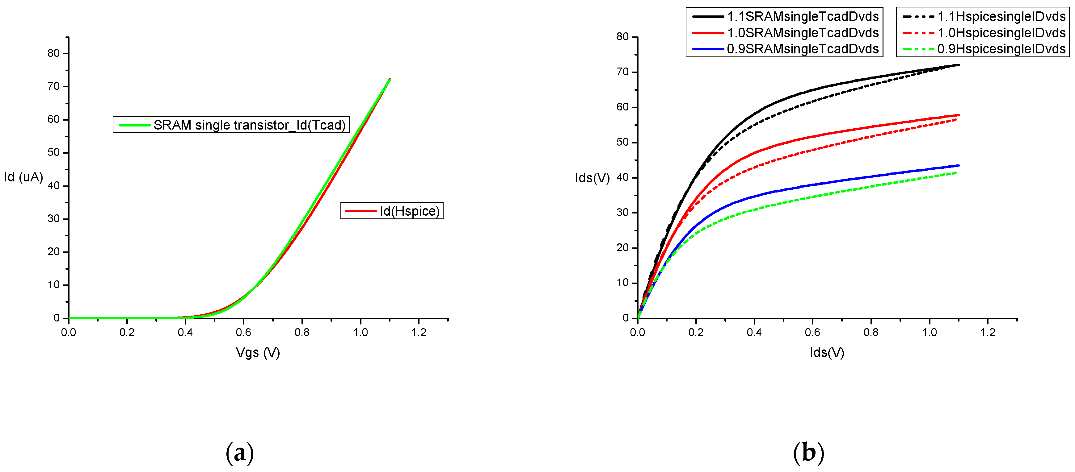
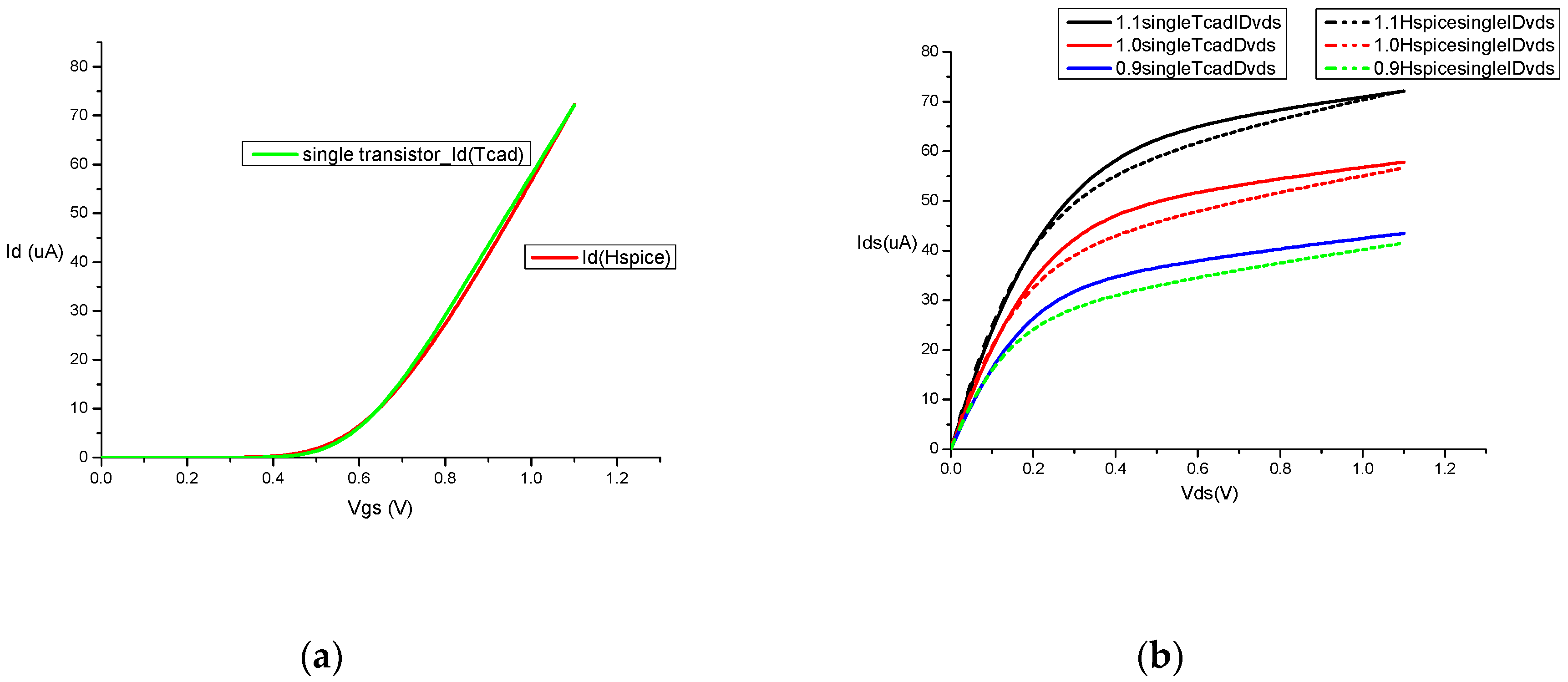
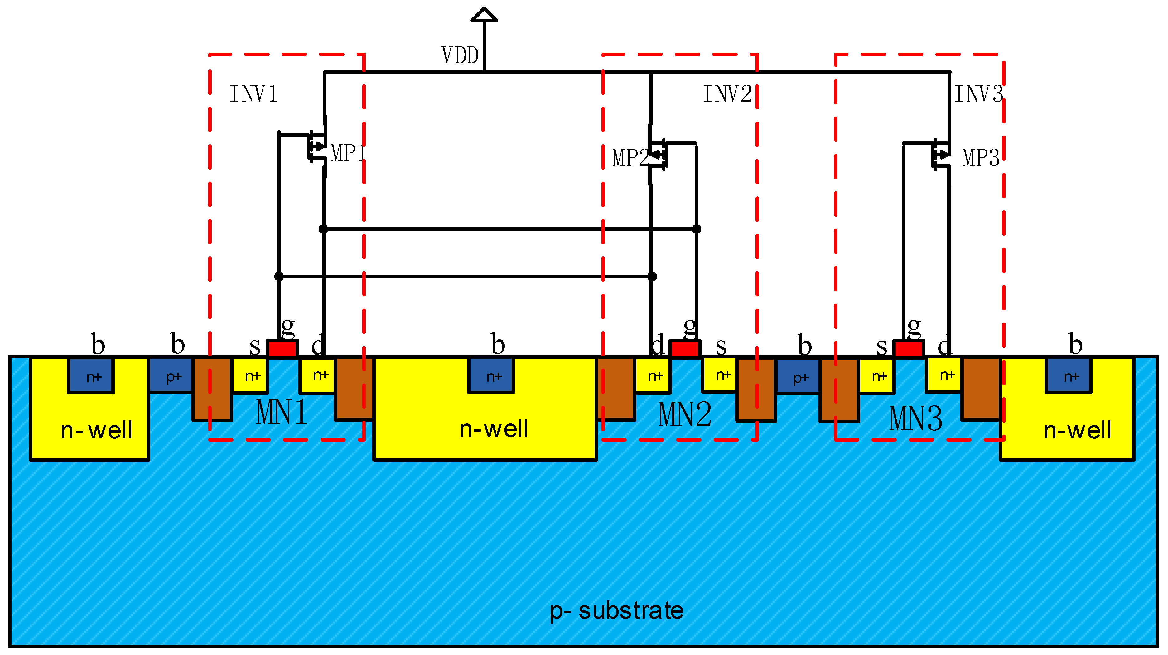
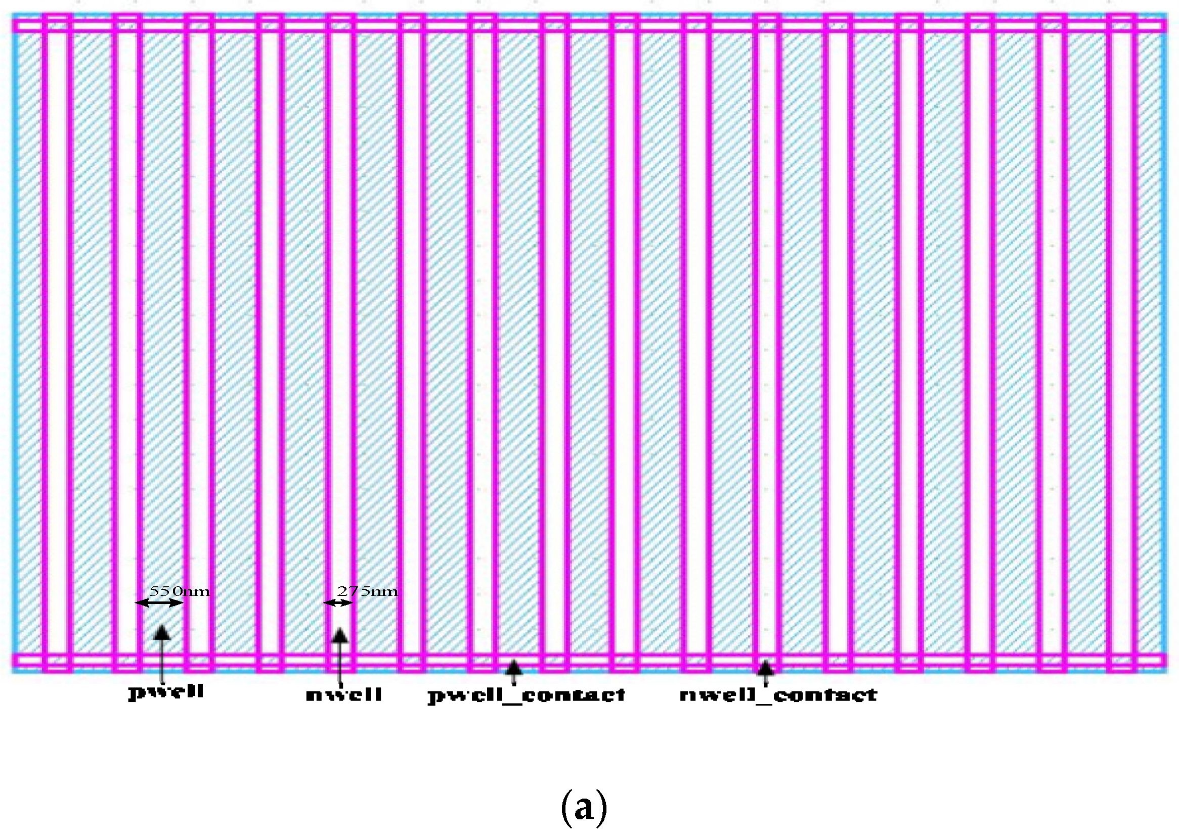
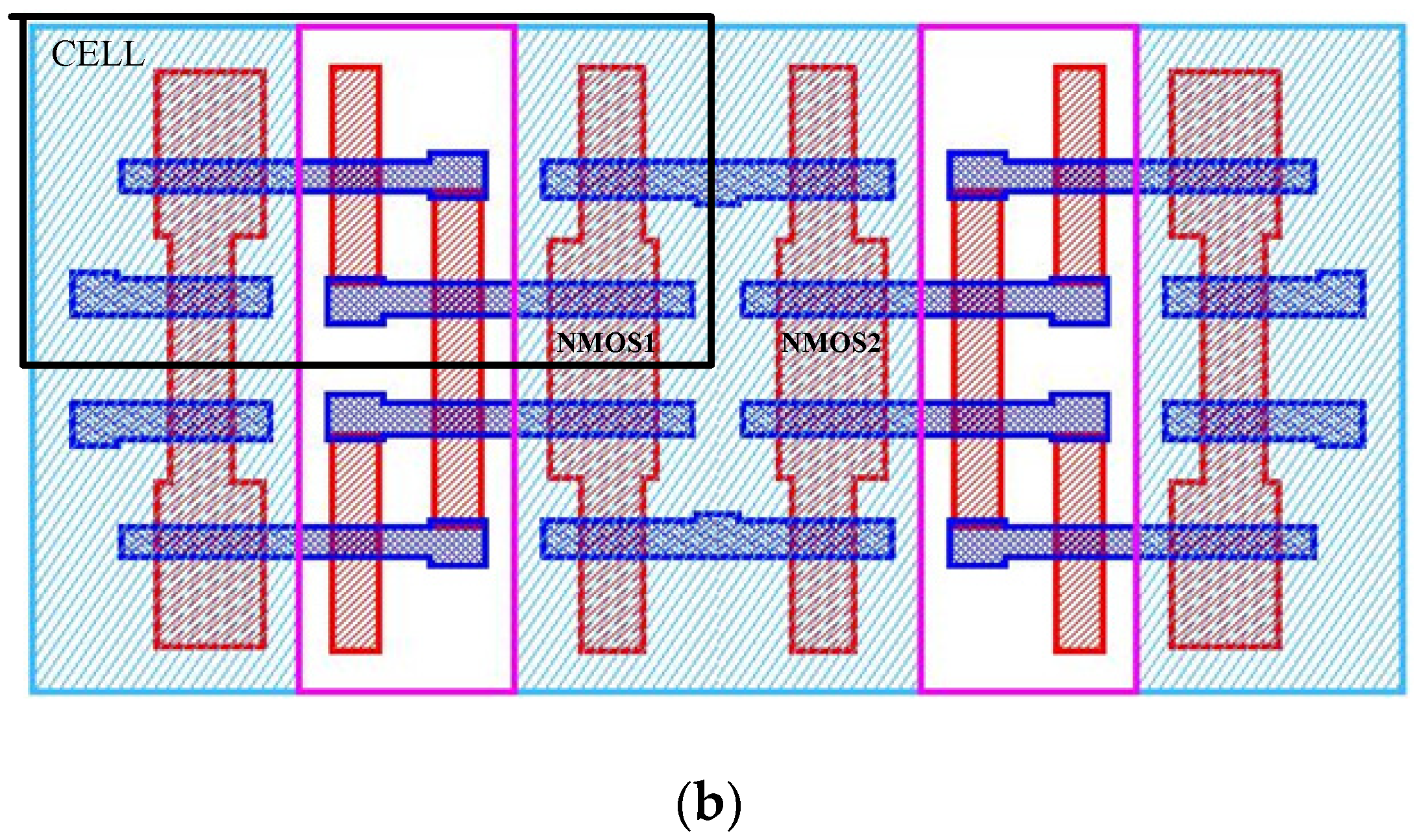
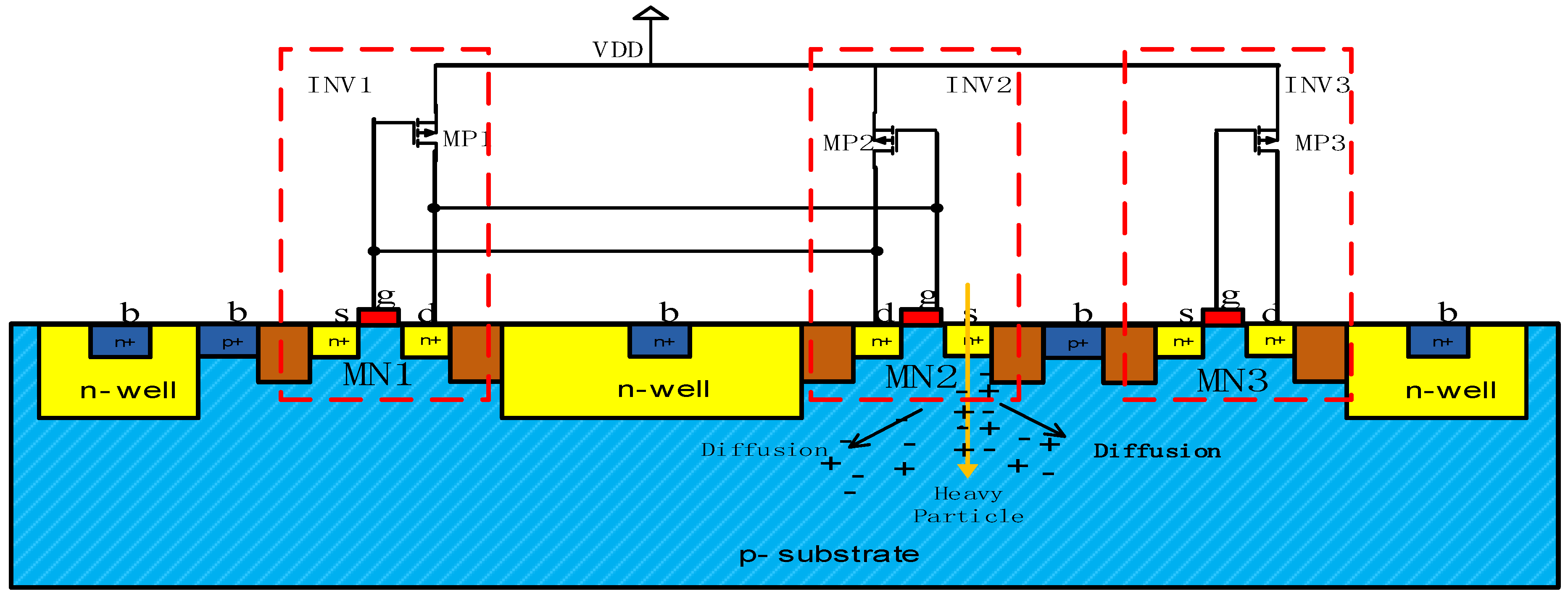
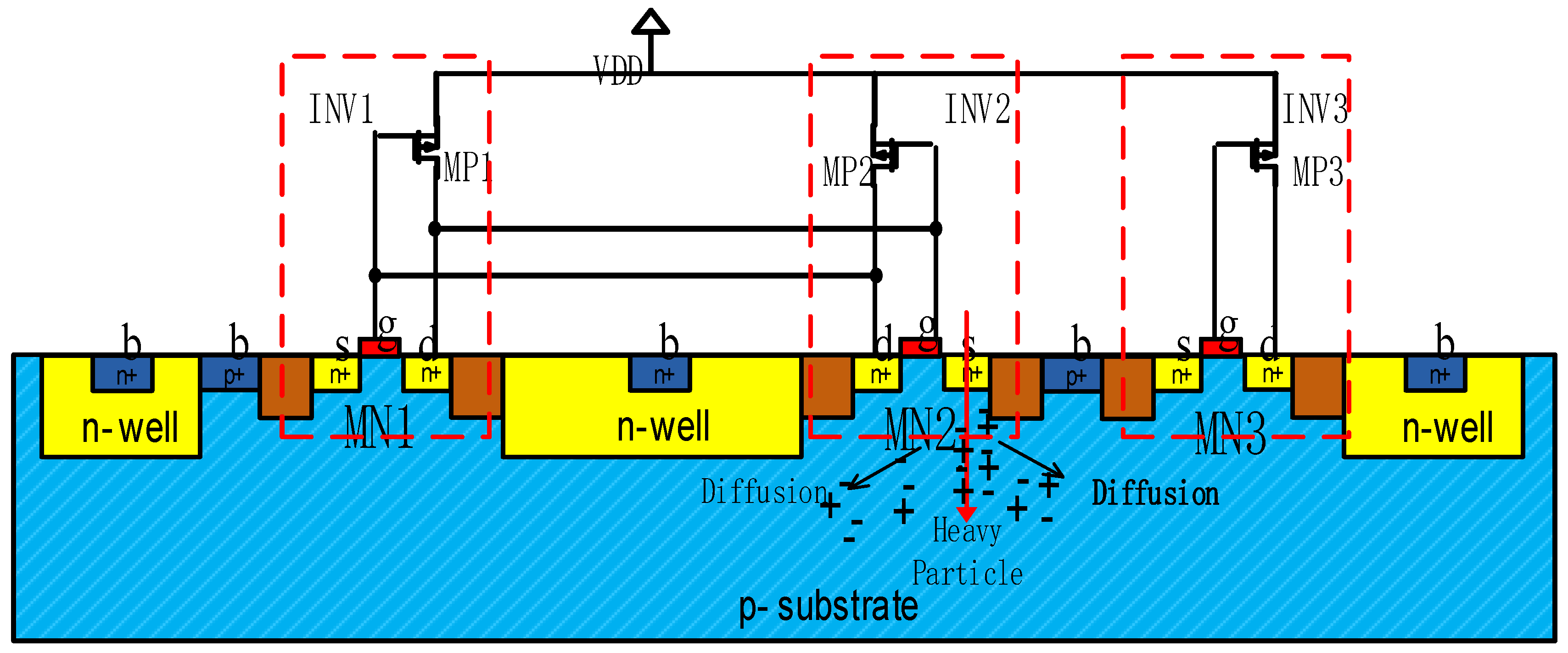
2. Device Model and I-V Curve Calibration

Sentaurus TCAD from Synopsys was used to model three devices and execute the emulations [15]. In this paper, mixed models were developed for the 40 nm SRAM. A TCAD structure was used for simulations as shown in Figure 1 [10,17]. The 3D view of the three NMOSFET is shown in Figure 1a. The cross-section view of a NMOSFET transistor is shown in Figure 1b. In the layout, a well contains 16 transistors, each of which belongs to a different storage cell [19]. The W/L ratio of the PMOSFET transistor is 0.055/0.06 μm in the SPICE lumped parameter model. The W/L ratio of NMOSFET is 0.055/0.192 μm in the TCAD distributed parameter model.
The TCAD model contained three NMOSFET transistors. These NMOSFET transistors were modeled with 3D digital models and were calibrated according to the commercial process design kits (PDKs) [10,17]. As shown in Figure 2 and Figure 3, the single NMOSFET of SRAM is calibrated according to the commercial PDKs.
The main circuit structure of a SRAM cell is shown in Figure 4. A mixed-mode model was developed using the structure shown in Figure 1. Figure 1 is not convenient to represent the striking schematic diagram, and Figure 5 is used to represent it. The main structure of a SRAM cell is composed of an interlocked inverter pair, such as INV1 and INV2. INV3 replaces another SRAM cell. The basic circuit is emulated in an initial state with MN2 and MP1 being in the OFF state and MN1 and MP2 being in the ON state. MN2 and MN3 can realize carriers sharing collection after particles strike [10,17].
The volume of silicon used for simulations is 5 μm × 5 μm × 5 μm. The incident particles are modeled using a Gaussian radial profile with 0.37 radius of 5 μm.

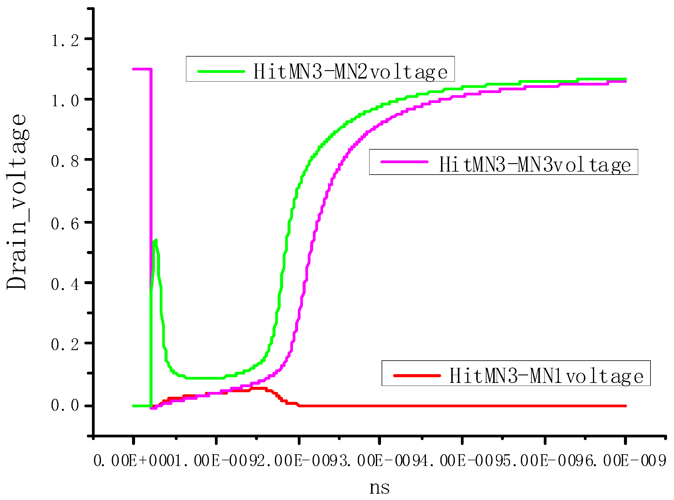
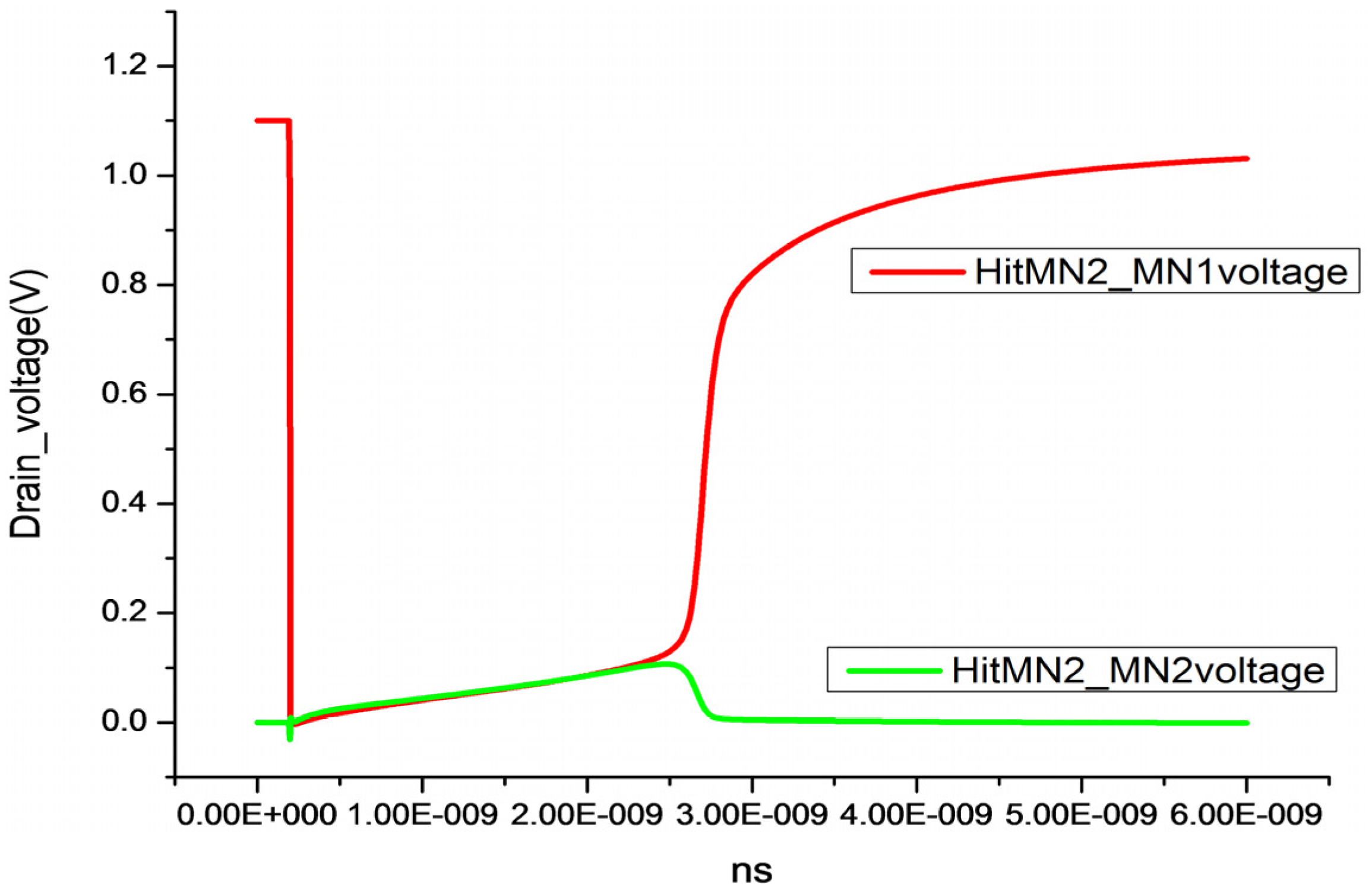
3. Emulation Voltage Waveform and Experimental Data

The layout, optimized for area at a 40 nm technology node, is used for SRAMs to estimate the single event response of the 40 nm technology node. SRAMs, but from one specific layout manufacturer, were exposed to heavy particles at the HI-13 Tandem Accelerator in the China Institute of Atomic Energy, Beijing. The simplified layouts of the SRAM are shown in 6a. The n- and p-wells are isolated from each other in the layout [19]. Each well is connected by one contact, and one well is placed every 16 rows. The nominal value for the 40 nm technology node is 1.1 V. The SRAM layout is simplified in Figure 6b; specific details are proprietary. Because interleaving techniques significantly increase the layout area, interleaving schemes were not used in the experimental chips.
The test was carried out with five heavy ions (Al, Cl, Ge, Li, and O) for the 40 nm technology node. Particle LET values were from 0.5 to 37.3 MeV cm2/mg. The range of particles in silicon was 30.5–249.9 μm. Table 1 contains the particle beams, particle LET values, particles energy, ranges in silicon [10,17], probability of single cell upset during single particle striking, and probability of multiple cell upset during single particle striking. In this paper, the particle incident on the drain region of transistor and carriers diffusion is shown in Figure 7. Numerous ionized carriers are generated along the particle track core [16,17].
The distance between two NMOS transistors in the same well is the minimum distance of two NMOS transistors according to the design rules to take advantage of the single event upset reversal (SEUR) caused by scaling trend. As shown in Figure 8, initially, the circuit was simulated with the drain of MN2 HIGH, MN1 LOW, and MN3 HIGH, which results from transistors MN2, MN3, and MP1 being in the OFF state, as well as MP2, MP3, and MN1 being in the ON state.
As shown in Figure 8, a particle strikes the drain central region of the MN2 transistor perpendicularly. The simulation results show the voltage changes at both the drains of MN1 and MN2, as shown in Figure 9. Initially, MN2 is in the OFF state; when it collects charge, the struck transistor (MN2) of inverter INV2 is ON. A series of state changes flips the MN1 in the inverter INV1.
As shown in Figure 10 and Figure 11, the drain central region of transistor MN3 was struck by a particle. The simulation results show the voltage changes for three NMOSFET drains of MN1, MN2, and MN3. At first, the MN2 was in OFF state; when it collected enough carriers, the MN2 in the inverter INV2 was in ON state, and the MN1 in the inverter INV1 switched into the OFF state. As shown in Figure 11, MN1 tried to recover, but the lack of sufficient charge prevented MN1 from reverting back to its initial state. The gate of transistor MN3 was connected to the GND. When the particle struck the drain central region of MN3 in the inverter INV3, MN3 collected carriers, and the output of inverter INV3 changed. After the excess carriers disappeared, the state of MN3 recovered.
SERs for SRAM depend on the critical charge collected by a sensitive node. For all technology processes, the critical charge depends on the technology process and active region doping. The critical charge is inversely proportional to active region doping. To keep a moderate threshold voltage for all technology processes, the channel doping and the well doping are increased with scaling down [10,17]. Thus, the charge collected by the 40 nm process is lower than that of 65 nm and higher than that of 28 nm; meanwhile, the space between transistors is moderate in the 40 nm technology process, and the probability of the MOS transistor collecting enough carriers to mitigate cell upset is beneficial for the 40 nm technology node. The structural layout also plays an important role for single event cell upset, as scaling down, the structural layout, and well engineering determine the soft error rate of SRAMs [10,17].
On the other hand, when a particle with high LET strikes at adjacent sensitive nodes, especially when multiple particles strike at adjacent sensitive nodes at the same time for the 40 nm technology node, the amount of charge available collected by the MN transistor is sufficient to return to the initial state. The space between transistors favors the charge collection [10]. These factors lead to the dominance of the upset reversal mechanism for the 40 nm technology process. As shown in Figure 12 and Figure 13, the drain voltage of MN1 recovered to its original state after MN2 was struck.
A custom SRAM was designed using a 40 nm technology node to verify the rate of single cell upsets and multiple cell upsets, which meets access functions. The chip used for features of single event upset (SEU) was a full custom SRAM, which was made up of four 128 × 32 × 4 × 8 bit blocks, 512 Kb. The experimental chip of SRAM with a 55AA pattern was irradiated using five heavy particles: Ge, Cl, Al, O, and Li. The experiments were carried out at the HI-13 Tandem Accelerator in the China Institute of Atomic Energy, Beijing. This SRAM was accessed at a frequency of 15 MHz, from the first word wire to the last word wire. It took 34 ms to access the test SRAM until the 1 × 10⁷ particles ran out. The number of irradiation particles per accessing cycle was about 4014 ions/cm2. The test area of the test SRAM chip was about 2 mm × 2.5 mm. The number of particles striking the chip per accessing cycle was about 200 particles [25]. The captured SCUs and MCUs were recorded after 1 × 10⁷ particles ran out.
When the full custom SRAM was accessed, the storage cells of the same address were accessed at the same time. When a storage cell upset was detected, the error was corrected through EDAC. After the last address was accessed, a new cycle was performed from the first address to the last address until the completion of 1 × 10⁷ particle strikes.
The field programmable gate array was responsible for the execution of the tests applied for SRAM. A computer was connected to the field programmable gate array in order to access the experimental data. The computer was located outside the radiation room. Experimental data were timely recorded and saved for subsequent processing. The total single cell upset events were 2,000,147, 1,124,269, 413,100, 311,311, and 47,815 under the irradiation of Ge, Cl, Al, O, and Li, respectively; the total multiple cell upset events were 10, 4, 0, 0, and 0 under the irradiation of Ge, Cl, Al, O, and Li, respectively [25]. The upset events decreased with LET decrease, and the multiple cell upsets events also decreased with LETs decrease. Single cell upset error rates under different particle striking are shown in Figure 14; multiple cell upsets are shown in Figure 15. The decreasing trend of the number of multiple cell upsets is attributed to the single event upset reversal, which was observed in the 40 nm technology node. To further reduce single cell upsets, the density of the well contact increased the maximum design density in the custom SRAM [20,21].

4. Conclusions

In this work, the feature of single cell upset in the full custom SRAM was carried out for a 40 nm bulk CMOS technology. The effect of structural layout and well engineering on single cell upset was researched and discussed on single event upset reversal under heavy particles exposure. The total single cell upset events were 2,000,147, 1,124,269, 413,100, 311,311, and 47,815 under the irradiation of Ge, Cl, Al, O, and Li, respectively. This indicates that single event cell upsets have become a major part of soft errors for the custom SRAM. The total multiple cell upset events were 10, 4, 0, 0, and 0 under the irradiation of Ge, Cl, Al, O, and Li, respectively. The results showed that multiple cell upsets significantly decreased. This indicates that the single event upset reversal mechanism plays a main role in SRAM and can be used for radiation hardening design. Moreover, there are a lot of single cell upsets appearing under Ge, Cl, Al, O, and Li exposure, the number may further increase with LETs increase. This shows that the well contacts still need optimization in the custom SRAM; for example, close spacing of well contacts or increasing contacts were used to drain the excess carriers quickly, and error detection and correction (EDAC) is used for SRAM technology. New radiation hardened by design techniques of SRAM need to be further proposed for single cell upset reduction, and the research on reduction techniques of SCUs continues in our group.

Author Contributions

Conceptualization, G.Y., Q.C.; methodology, G.Y., J.Z., Q.C., J.Y.; validation, G.Y., J.Z., X.L.; simulation, Q.C., J.Y.; formal analysis and investigation, X.L., J.Y.; writing original draft preparation, writing and editing, G.Y., J.Y., Q.C.; visualization and supervision, G.Y., J.Z. All authors have read and agreed to the published version of the manuscript.

Funding

This work is funded by the National Key R&D Program of China, grant number 2016YFB0400100-05.

Conflicts of Interest

The authors declare no conflicts of interest.

References

  1. Jan, M.; Chandrakasan, R.A.; Nikolic, B. Designing Memory and Array Structure. In Digital Integrated Circuits: A Design Perspective, 2nd ed.; Pearson Eeducation, Inc.: Upper Saddle River, NJ, USA, 2017; p. 625. [Google Scholar]
  2. Jeon, S.H.; Lee, S.; Baeg, S.; Kim, I.; Kim, G. Novel Error Detection Scheme With the Harmonious Use of Parity Codes, Well-Taps, and Interleaving Distance. IEEE Trans. Nucl. Sci. 2014, 61, 2711–2717. [Google Scholar] [CrossRef]
  3. Jing, G. Single Event Upsets Harden by Design Technology Research of Static Random Access Memory. Ph.D. Thesis, Harbin Institute of Technology, Harbin, China, 1 May 2015. [Google Scholar]
  4. Black, J.D.; Dodd, P.E.; Warren, K.M. Physics of Multiple-Node Charge Collection and Impacts on Single-Event Characterization and Soft Error Rate Prediction. IEEE Trans. Nucl. Sci. 2013, 60, 1836–1851. [Google Scholar] [CrossRef]
  5. Chen, J.; Liang, B.; Chi, Y. Experimental characterization of the bipolar effect on P-hit single-event transients in 65 nm twin-well and triple-well CMOS technologies. Sci. China Ser. E Technol. Sci. 2016, 59, 488–493. [Google Scholar] [CrossRef]
  6. Zhang, J.; Chen, J.; Huang, P.; Li, S.; Fang, L. The Effect of Deep N+ Well on Single-Event Transient in 65 nm Triple-Well NMOSFET. Symmetry 2019, 11, 154. [Google Scholar] [CrossRef] [Green Version]
  7. Zhang, J.; Fang, L.; Chen, J.; Hou, S.; Tong, X. Single Event Transient Study of pMOS Transistors in 65 nm Technology With and Without a Deep n+ Well Under Particle Striking. IEEE Access 2019, 7, 149255–149261. [Google Scholar] [CrossRef]
  8. Jagannathan, S.; Gadlage, M.J.; Bhuva, B.L.; Schrimpf, R.D.; Narasimham, B.; Chetia, J.; Ahlbin, J.R.; Massengill, L.W. Independent Measurement of SET Pulse Widths From N-Hits and P-Hits in 65-nm CMOS. IEEE Trans. Nucl. Sci. 2010, 57, 3386–3391. [Google Scholar] [CrossRef]
  9. Roy, T.; Witulski, A.F.; Schrimpf, R.D.; Alles, M.L.; Massengill, L.W. Single Event Mechanisms in 90 nm Triple-Well CMOS Devices. IEEE Trans. Nucl. Sci. 2008, 55, 2948–2956. [Google Scholar] [CrossRef] [Green Version]
  10. Chatterjee, I.; Narasimham, B.; Mahatme, N.N.; Bhuva, B.L.; Schrimpf, R.D.; Wang, J.K.; Bartz, B.; Pitta, E.; Buer, M. Single-Event Charge Collection and Upset in 40-nm Dual- and Triple-Well Bulk CMOS SRAMs. IEEE Trans. Nucl. Sci. 2011, 58, 2761–2767. [Google Scholar] [CrossRef]
  11. Huang, P.; Chen, S.; Chen, J.; Liu, B. Novel N-hit single event transient mitigation technique via open guard transistor in 65nm bulk CMOS process. Sci. China Ser. E Technol. Sci. 2012, 56, 271–279. [Google Scholar] [CrossRef]
  12. Chen, J.; Chen, S.; Liang, B.; Liu, F. Single event transient pulse attenuation effect in three-transistor inverter chain. Sci. China Ser. E Technol. Sci. 2012, 55, 867–871. [Google Scholar] [CrossRef]
  13. Huang, P.; Chen, S.; Liang, Z.; Chen, J.; Hu, C.; He, Y. Mirror image: Newfangled cell-level layout technique for single-event transient mitigation. Chin. Sci. Bull. 2014, 59, 2850–2858. [Google Scholar] [CrossRef]
  14. Wang, H.-B.; Bi, J.-S.; Li, M.-L.; Chen, L.; Liu, R.; Li, Y.-Q.; He, A.-L.; Guo, G. An Area Efficient SEU-Tolerant Latch Design. IEEE Trans. Nucl. Sci. 2014, 61, 3660–3666. [Google Scholar] [CrossRef]
  15. Zhang, K.; Kobayashi, K.; Kobayashi, K. Contributions of charge sharing and bipolar effects to cause or suppress MCUs on redundant latches. In Proceedings of the 2013 IEEE International Reliability Physics Symposium (IRPS), Monterey, CA, USA, 14–18 April 2013; p. 997. [Google Scholar]
  16. Luo, Y.H.; Zhang, F.Q.; Guo, H.X.; Zhou, H.; Zheng, L.S.; Ji, D.M.; Shen, C.; Gong, D.; Hajdas, W. Single event cluster multi-bit upsets due to localized latch-up in a90 nm COTS SRAM containing SEL mitigation design. IEEE Trans. Nucl. Sci. 2014, 61, 1918–1923. [Google Scholar]
  17. Chatterjee, I.; Narasimham, B.; Mahatme, N.N.; Bhuva, B.L.; Reed, R.A.; Schrimpf, R.D.; Wang, J.K.; Vedula, N.; Bartz, B.; Monzel, C. Impact of Technology Scaling on SRAM Soft Error Rates. IEEE Trans. Nucl. Sci. 2014, 61, 3512–3518. [Google Scholar] [CrossRef]
  18. Georgakos, G.; Huber, P.; Ostermayr, M.; Amirante, E.; Ruckerbauer, F. Investigation of Increased Multi-Bit Failure Rate Due to Neutron Induced SEU in Advanced Embedded SRAMs. In Proceedings of the 2007 IEEE Symposium on VLSI Circuits, Kyoto, Japan, 14–16 June 2007; pp. 80–81. [Google Scholar]
  19. Chen, H.; Chen, J.; Yao, L. Characterization of single-event multiple cell upsets in a custom SRAM in a 65 nm triple-well CMOS technology. Sci. China Ser. E: Technol. Sci. 2015, 58, 1726–1730. [Google Scholar] [CrossRef]
  20. Ibe, E.; Chung, S.S.; Wen, S.; Yamaguchi, H.; Yahagi, Y.; Kameyama, H.; Yamamoto, S.; Akioka, T. Spreading Diversity in Multi-cell Neutron-Induced Upsets with Device Scaling. In Proceedings of the IEEE Custom Integrated Circuits Conference, San Jose, CA, USA, 10–13 September 2006; pp. 437–444. [Google Scholar]
  21. Furuta, J.; Kobayashi, K.; Onodera, H.; Kobayashi, K. Impact of cell distance and well-contact density on neutron-induced Multiple Cell Upsets. In Proceedings of the 2013 IEEE International Reliability Physics Symposium (IRPS), Monterey, CA, USA, 14–18 April 2013; pp. 6C.3.1–6C.3.4. [Google Scholar]
  22. Zhangd, K.; Furuta, J.; Kobayashi, K.; Onodera, H.; Zhang, K. Dependence of Cell Distance and Well-Contact Density on MCU Rates by Device Simulations and Neutron Experiments in a 65-nm Bulk Process. IEEE Trans. Nucl. Sci. 2014, 61, 1583–1589. [Google Scholar] [CrossRef]
  23. Song, Y.; Vu, K.; Cable, J.; Witteles, A.; Kolasinski, W.; Koga, R.; Elder, J.; Osborn, J.; Martin, R.; Ghoniem, N. Experimental and analytical investigation of single event, multiple bit upsets in poly-silicon load, 64 K*1 NMOS SRAMs. IEEE Trans. Nucl. Sci. 1988, 35, 1673–1677. [Google Scholar] [CrossRef]
  24. Black, J.D.; Ii, D.R.B.; Robinson, W.H.; Fleetwood, D.M.; Schrimpf, R.D.; Reed, R.A.; Black, D.A.; Warren, K.M.; Tipton, A.D.; Dodd, P.E.; et al. Characterizing SRAM Single Event Upset in Terms of Single and Multiple Node Charge Collection. IEEE Trans. Nucl. Sci. 2008, 55, 2943–2947. [Google Scholar] [CrossRef]
  25. Gasiot, G.; Roche, P.; Flatresse, P. Comparison of multiple cell upset response of BULK and SOI 130NM technologies in the terrestrial environment. In Proceedings of the 2008 IEEE International Reliability Physics Symposium, Phoenix, AZ, USA, 27 April–1 January 2008; pp. 192–194. [Google Scholar]
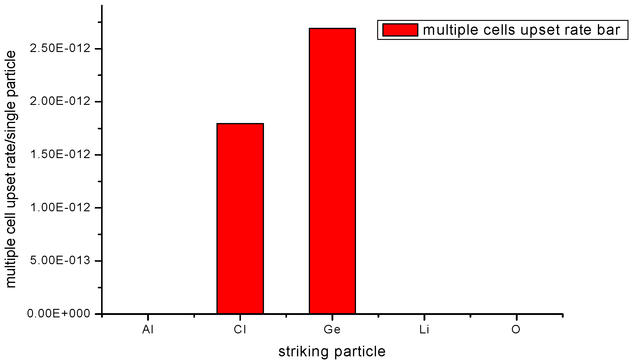
Figure 1. NMOS TCAD structure: (a) 3D view and (b) 2D cross-section view.
Electronics 09 00927 g001
Figure 2. A single transistor of a static random access memory (SRAM) cell: (a) Id–Vg curves calibrated, (b) Id–Vd curves calibrated.
Electronics 09 00927 g002
Figure 3. A single transistor: (a) Id–Vg curves calibrated, (b) Id–Vd curves calibrated.
Electronics 09 00927 g003
Figure 4. The main circuit structure of a SRAM cell.
Electronics 09 00927 g004
Figure 5. Particle strike the drain of NMOSFET transistor in a storage cell of SRAM.
Electronics 09 00927 g005
Figure 6. (a) Layout of the SRAM, (b) structural layout of the 6 transistors cell.
Electronics 09 00927 g006aElectronics 09 00927 g006b
Figure 7. A particle strikes the drain of transistor and carriers diffuse.
Electronics 09 00927 g007
Figure 8. A particle strikes the drain central region of MN2 transistor perpendicularly. Cross-sections of layout in a cell of SRAM.
Electronics 09 00927 g008
Figure 9. Drain voltages of MN1 and MN2 when the drain of MN2 is struck by a particle.
Electronics 09 00927 g009
Figure 10. A particle strikes the drain central region of MN3 transistor perpendicularly. Cross-sections of layout in a cell of SRAM.
Electronics 09 00927 g010
Figure 11. Drain voltage in MN1, MN2, and MN3 transistors when the drain central region of nMOS transistor MN2 is struck by a particle.
Electronics 09 00927 g011
Figure 12. A particle strikes the drain region of MN2 transistor perpendicularly. Cross-sections of layout in a cell of SRAM.
Electronics 09 00927 g012
Figure 13. Drain voltage of MN1 and MN2 transistors after the drain central region of the nMOS transistor MN2 is struck with a particle.
Electronics 09 00927 g013
Figure 14. Single cell upsets (SCUs) versus particles for 512 Kbit SRAM with a 55AA pattern for normal incidence irradiation operated at 1.1 V.
Electronics 09 00927 g014
Figure 15. Multiple cell upsets (MCUs) versus particles for 512 Kbit SRAM with a 55AA pattern for normal incidence irradiation operated at 1.1 V.
Electronics 09 00927 g015
Table 1. Parameter of particles.
ParticleEnergy
(MeV)
LET (Mev/mg/cm2)Range
(μm)
SCU (cm2/Particle)MCU (cm2/Particle)
Ge21037.330.58.97617E-72.69265E-12
Cl16013.146.05.04544E-71.7951E-12
Al1208.650.01.85389E-70
O1003.195.21.39709E-70
Li440.5249.92.14582E-80

