Article

The Improvement Switching Technique for High Step-Up DC-DC Boost Converter

HCMC University of Technology and Education, Ho Chi Minh City 71307, Vietnam
*
Author to whom correspondence should be addressed.
Electronics 2020, 9(6), 981; https://doi.org/10.3390/electronics9060981
Submission received: 9 May 2020 / Revised: 4 June 2020 / Accepted: 9 June 2020 / Published: 12 June 2020
(This article belongs to the Section Power Electronics)

Abstract

:
This paper proposes the non-isolated DC-DC converter with high boost ratios and efficiency. We suggest boosting methods including voltage multiplier cells or coupled inductors. However, both techniques have a limited constant voltage multiplier coefficient according to the fixed configuration. Therefore, in the proposed method, we change the multiplier factor (as the number of activity levels) and combine it with the turn of the appropriate duty cycle; these factors are considered at the same time in order to increase the energy conversion efficiency and expand the control area of the duty cycle. A mathematical analysis of the losses of the components in operation modes shows that the boost ratio and efficiency are functions of the number of activity levels and duty cycle. Therefore, this paper proposes an algorithm for tracking the activity levels and duty cycle in order to obtain the maximum efficiency. The simulations produced with the Powersim-PSIM software, and the experiments with load capacities of 250 W, 500 W and 1000 W, boosting the ratio by more than ten times, were conducted in order to clarify the capabilities of the proposed configuration.

Graphical Abstract

1. Introduction

High step-up DC-DC converters have various applications, such as uninterrupted power supply-UPS, renewable energy systems, fuel cell systems, and hybrid electric vehicles [1,2,3,4,5,6,7,8,9]. They can be classified into two types: isolation and non-isolation converters [10,11,12]. Isolated DC-DC converters have some disadvantages, such as high eddy current and voltage stress on the output diode [12]. When applications do not have the required isolation, non-isolated DC-DC converters offer a more straightforward and flexible solution for boosting [10,11].
Conventional DC-DC converters include an inductor, a switch and a diode, as shown in Figure 1a. For a high boost ratio, it operates at an extreme duty cycle D (to units). The boost ratio may be higher if more conventional boost converters cascade, as shown in Figure 1b,c. Theoretically, these cascading converters are another technique for obtaining a higher boost ratio and lower conductive losses without an extreme duty cycle. However, these converters still suffer from high voltage stress and the significant input current ripple of DC power [13].
To reduce the input current ripple, a two-phase interleaved boost converter with parallel inputs and parallel boosters is proposed, as shown in in Figure 1d. The switches S1 and S2 in Figure 1d are activated alternately so that the input current’s ripple is lower [14].
In recent years, studies of high step-up DC-DC converters have been published with improved topologies to reduce the input ripple current (voltage lift cell (VLC) and interleaved input), incorporating voltage multiplier cells or coupled inductors [15,16,17], as shown in Figure 1e, Figure 2a,b. Although it has the advantages of high voltage gain, the configuration shown in Figure 1e has a larger size and weight [18]. Another improved technique which uses a voltage multiplier circuit is illustrated in Figure 2a,b.
The voltage multiplier has some of the diodes and capacitors. Theoretically, it is possible to use more capacitors and diodes in order to obtain a larger voltage boost ratio. Therefore, this circuit can increase the output boost at a low duty cycle. According to [16], the boost ratio can be determined as (1)
B = U L E = 2 N 1 D
Another improved configuration, as shown in Figure 2b, with the voltage lift cell (VLC) includes two inductors L1, L2, two diodes D1, D2 and a capacitor C1, replacing the interleaved input. In this structure, not only is the number of switches reduced, but the voltage boost ratio is also twice as high, as shown in the Formula (2).
B = U L E = 4 N 1 D
With Cockcroft–Walton cells, the energy is transferred between the capacitors (for example, from C3 to C2 Figure 2b) in a short period of time so that the power loss on the capacitor is high while the conversion efficiency reduces.
Using VLCs reduces the number of switches but increases the current that passes through them. Therefore, the loss of the switch with the VLC is greater than the interleaved input.
Now, the improved converters with a high boost ratio and a low ripple current are shown in Table 1.
This shows that the voltage multiplier ratio N is not changed in operation. Thus, the only way to change the boost ratio is to regulate the duty cycle D. As a result of this limitation, there are not many flexibilities of control and implementation optimizations.
Thus, this paper proposes an improved DC-DC converter topology with an interleaved input, high boost ratio and flexible control according to the optimized functions and fewer multipliers. The two parameters that can be regulated to achieve the desired voltage boost are the duty cycle D and the voltage multiplier N.

2. The Improvement Switching Technique

This paper proposes an improved DC-DC converter that uses the cascaded traditional boost circuit, with a high voltage boost ratio, wide control range and optimal control. Moreover, a new control method is shown with an almost linear and stable output voltage. The control technique is flexible because of the wide control range with two variants of the duty cycle D and the voltage multiplier N.
Figure 3 shows that the proposed converter has some of the basic cascaded levels such as an inductor, MOSFET, diode and capacitor. The inductor is the energy store that is magnetized during turn-on time and demagnetized during turn-off time; the diode is used to direct the currents, and the capacitor acts to charge and discharge the energy.

2.1. Principles

Set Nmax is the number of levels in the configuration, which means that Nmax will be four with the converter, as shown in Figure 3a. The three stages of the converter are described in Figure 3b–d. Figure 4 shows the waveform of the voltage and current on switches, inductors and capacitors in the switching cycle. The first level always acts while the other might be active or not, depending on the status of the switches. There are four operation modes in the converter, as shown in Table 2.
This section analyzes the first mode with full activity levels. Figure 4 shows the established waveforms in the switching cycle of the converter in the first mode. In this case, all of the levels operate together. The control cycle of S1 is the same as S3 and the phase shifts by 180° between S2 and S4. In the first mode, there are three operating states, which are shown in Table 3.
In stage 1, from t1 to t2, the MOSFETs turn on, the diodes turn off and four inductors are magnetized by the input source (Figure 3b). Therefore, the current that is charged into the inductor linearly increases and can be calculated using the following Formulas (3) and (4). The output capacitor (C4) supplies energy to the load.
i L 1 ( t ) = I L 1 ( t 0 ) + V i n L 1 ( t t 0 ) and i L 3 ( t ) = I L 3 ( t 0 ) + V i n L 3 ( t t 0 )
i L 2 ( t ) = I L 2 ( t 0 ) + V i n L 2 ( t t 0 ) and i L 4 ( t ) = I L 4 ( t 0 ) + V i n L 4 ( t t 0 )
State 2 [t2–t3]: the two switches S1 and S3 turn off while the remaining switches (S2, S4) still turn on (Figure 3c). The capacitor C1 is charged by the energy stored in L1 and the power source, similar to the C3 in level 3. The inductor in levels 2 and 4 still magnetizes so that the current that passes through S2 and S4 is the sum of the inductor’s magnetized current and the capacitor’s charging current. The output capacitor (C4) supplies energy to the load:
V C 1 = V S 1 = V S 3 = V i n 1 D
V C 3 = V C 2 + V i n 1 D = 3 V i n 1 D
State 3 [t3–t1]: this state is the same as state 2 with the status of switches and capacitors on the reverse. Both capacitors C1 and C3 transfer energy to capacitors C2 and C4, respectively. The output capacitor C4 still supplies the load. In this state, the S1 current is only the L1’s magnetized current.
V S 2 = V S 4 = V i n 1 D
V C 2 = 2 V i n 1 D
V C 4 = V C 3 + V i n 1 D = 4 V i n 1 D
Consequently, the voltage boost factor depends on the activity levels (N). The ideal voltage boost ratio B* can be determined by the Formula (10),
B * = V C o V i n = N 1 D = I i n I o   w h e r e   N = 1 ,   2 , , N m a x
The switch voltage stress (at the current level) is:
V S 1 = V S 2 = V S 3 = V S 4 = V i n 1 D
The voltage across on the diode can be calculated based on the analysis of stage 2 and stage 3:
{ V D 1 = V i n 1 D V D i = i V i n 1 D   k h i   i < N V D i = 0   k h i   i > N

2.2. Power Loss Analysis

The resistors RD, RL, RS can be described as the resistance of the turn-on diode, the inductor and the turned-on switch.

2.2.1. Power Loss in Diode:

All diodes are turned on in the ( 1 D ) T period with the current the same as the level current at the corresponding stage. Therefore, the conductive losses on the diode can be calculated by:
Δ P D = N ( 1 D ) R D I D 2 = N R D I o 2 1 D
where N is the number of the activity levels and Io is the load current.

2.2.2. Power Loss in Inductor:

The power losses in the inductors consist of two main losses: copper and core losses. The sum of the two losses can be represented by a resistor. The currents that pass through the inductor in all stages can be presented as the mean current on the level. Therefore, the losses in the N inductors can be calculated as:
Δ P L = N R L I L 2 = N R L I o 2 ( 1 D ) 2

2.2.3. Power Loss in the Switch:

The power loss in switch S1 can be calculated similarly to the traditional boost circuit using the Formula (15).
Δ P S 1 = D R S I S 1 2 = D R S I o 2 ( 1 D ) 2
At levels 2 to 4, the current on the turned-on switch is also the current on the inductor in stage 1. Consequently,
Δ P S i ( S 1 ) = ( 2 D 1 ) R S I S ( S 1 ) 2 = ( 2 D 1 ) R S I o 2 ( 1 D ) 2 ,   i = 2 4
However, in stages 2 and 3, during ( 1 D ) T , the switch current is the magnetization and charge of the front level capacitor (Figure 4). Therefore, the power losses in the switches in these stages can be calculated, respectively, as:
Δ P S i ( S 2 _ 3 ) = ( 1 D ) R S I S ( S 2 ) 2 = ( 1 D ) R S 4 I o 2 ( 1 D ) 2 = R S 4 I o 2 ( 1 D ) ,   i = 2 4  
Consequently, the total loss in a switch (S2, S3 or S4) in a cycle is:
Δ P S i = ( 3 2 D ) R S I o 2 ( 1 D ) 2

2.2.4. Power Loss in the Output Capacitor

The output capacitor (C4) serves not only to store energy but also to supply it to the load. The output capacitor current has two components, namely the charge and discharge currents. The C4 discharge current is the load current, and the charge current is the difference between the last level and the output current. Therefore, this can be calculated as (19):
Δ P C 4 = D R C I o 2 1 D

2.2.5. Losses in the Level Capacitor:

The level capacitors (C1 to C3) operate in stages 2 and 3 only. Both the charge and discharge currents of them are involved in the inductor current sequence. Thus, the power losses to the level capacitor can be calculated as (20)
Δ P C i = 2 R C I o 2 1 D
According to [19], conductive losses are low when switching frequencies below 100 kHz, which can lead to the switching losses being ignored. Consequently, the total power loss in the proposed circuit can be calculated by the following:
Δ P = Δ P L + Δ P S + Δ P D + Δ P C = N R L ( 1 D ) 2 I o 2 + D + ( N 1 ) ( 3 2 D ) R S ( 1 D ) 2 I o 2 + N m a x R D 1 D I o 2 + D + 2 ( N 1 ) R C 1 D I o 2

2.3. Control Technology to Minimize Power Loss

In order to maximize the conversion efficiency, it is necessary to determine the correct values of N and D for minimizing the power losses defined by the Formula (21) on the conditions in (22).
{ 1 N N m a x   ( N ) 0.1 D 0.8   i f   N = 1 0.5 D 0.8   i f   N > 1
The Formula (21) is rewritten as below.
Δ P = I o 2   ( N R L ( 1 D ) 2 + D + ( N 1 ) ( 3 2 D ) R S ( 1 D ) 2 + N m a x R D 1 D + D + 2 ( N 1 ) R C 1 D )
If set up internal resistance:
r o = N R L ( 1 D ) 2 + D + ( N 1 ) ( 3 2 D ) R S ( 1 D ) 2 + N m a x R D 1 D + D + 2 ( N 1 ) R C 1 D
Thus:
Δ P = I o 2 r o
Alternatively:
Δ P = I o 2 r o = ( P o V o ) 2 r o = ( V o R L o a d ) 2 r o
Therefore, with the required output power Po and output voltage Vo (respectively Io and RLoad), the choice of working levels N and duty cycle D to minimize power losses is, in fact, essentially minimum internal resistance ro. The efficiency of the circuit can be calculated according to Equation (27). B* is the ideal voltage boost ratio in (10), and the internal resistance (ro) is zero. The efficiency can be calculated by
η = P o P i n = V o I o V i n I i n = V o I o V i n I o B * = V o V i n B *
The real voltage boost B = V o V i n is set up, then
B = V o V i n = η B *
The input power Pin and output voltage Vo are also calculated as follows:
P i n = P 0 + Δ P
V o = V i n B * ( N , D ) I o r o  
This paper proposes using a graph method to determine N and D for minimum ΔP (or minimum internal resistance ro). The value of r0 as calculated in Formula (24) with the parameters RL, RS, RD, RC is given in Table 5. The values D and N satisfy the constraint (22). The real voltage boost B can be calculated by Formula (28) for each value of N, D, and ro.
The load resistor RLoad can be calculated from the required output voltage and power of the DC-DC converter in Equation (31). We select RLoad = 250 Ohm, which is suitable for Vo from 400 V to 600 V and Po from 250 W to 1000 W.
R L o a d = V o 2 P o
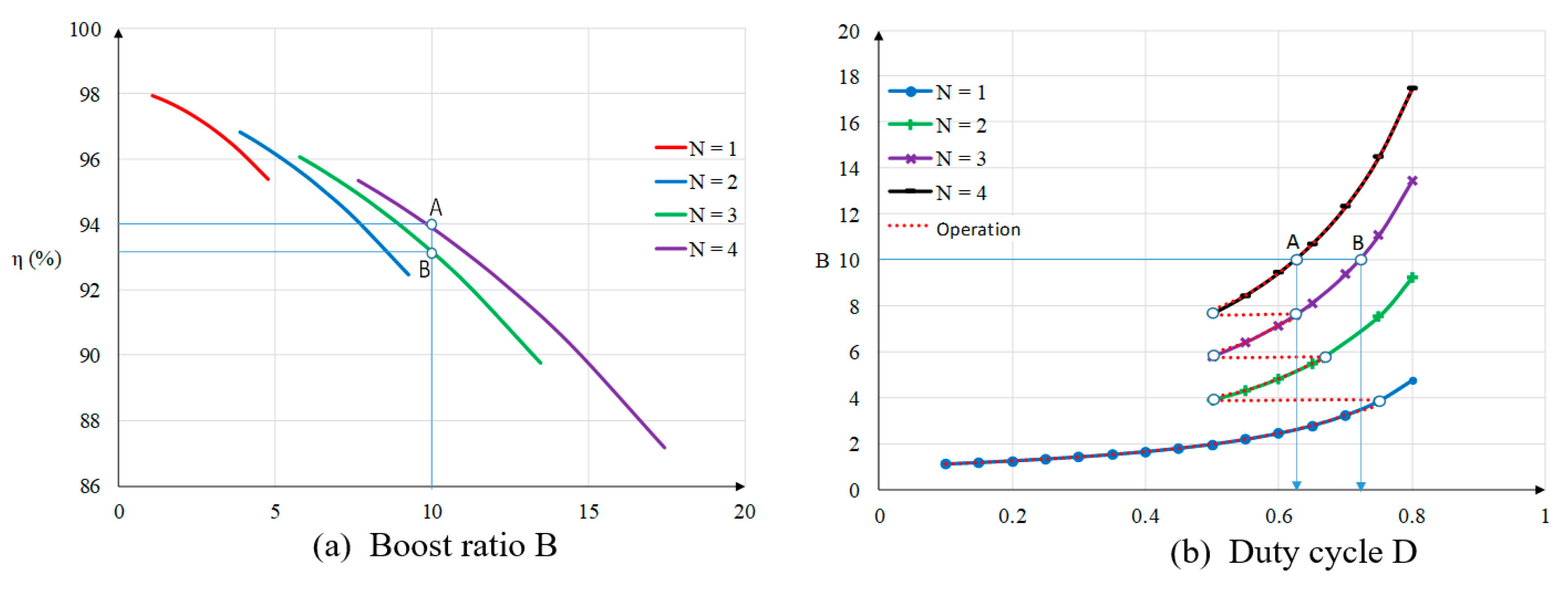
The efficiency and boost ratio graphs according to the activity levels N and duty cycle D are indicated by the flowchart in Figure 5, and Figure 6 shows the results of this.
Thus, using the figures in Table 4, it is possible to quickly determine the number of working levels of N and the appropriate range of D so that the conversion efficiency is the highest.

3. Simulation and Experimental Results

3.1. Experimental Model and Results

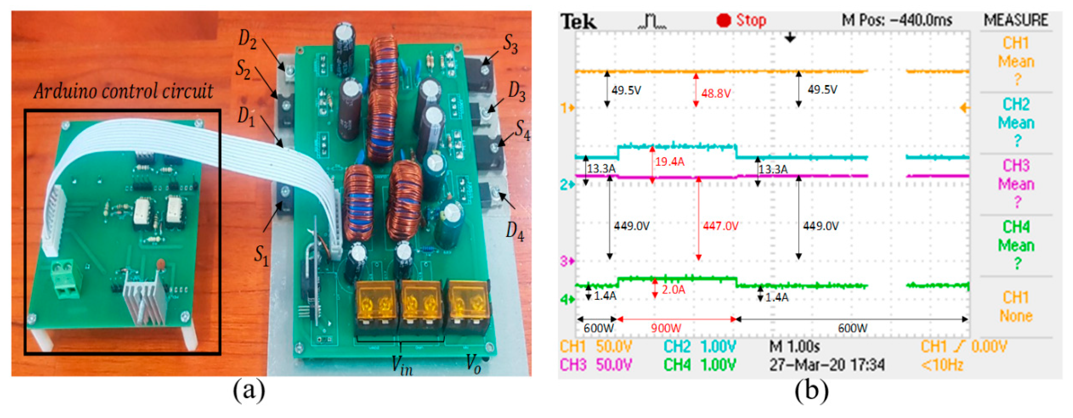
The experimental model in Figure 7a has a design capacity of 1000 W and a maximum input voltage of 70 V at four levels. Table 5 shows the circuit parameters. Practical experiments were conducted with various different loads. Figure 7b shows the current and voltage values measured by the oscilloscope in the boost ratio B = 9 and the load changes from 600 W to 900 W. In Figure 7b, the orange and blue lines are the input voltage and current while the green and violet lines are the output current and voltage sequence. The measurement results are shown in Table 6. The efficiencies calculated from the measurement data are 95.5% and 94.4% at the 600 W and 900 W sequences.
The three loads that were measured in the simulation and experiment were 1000 W, 500 W and 250 W. We performed some experimental and simulated tests to verify the findings, including the following:
Test 1: Determine the duty cycle (D) and the number of activity levels (N) while changing the boost ratio B. This test shows the benefits of flexibility when combining the duty cycle and the number of activity levels. The duty cycle is always in the controllable area (in Table 5) by increasing or decreasing working levels. Then, it is easy to control the stable output voltage under the changing of the load or the input voltage.
Test 2: Determine the conversion efficiency η according to the voltage boost ratio B. This test shows that an advantage of the proposed technique is its ability to possibly increase the conversion efficiency if the duty cycle and the number of activity levels are determined appropriately. The selection of the largest number of activity levels, if possible, will reduce the current through the components, thus helping to increase the conversion efficiency.

3.2. Analysis of the Results of Tests 1 and 2 with the Load of 500 W

Figure 8a shows four characteristics of the boost ratio B with four values of N (N = 1 … 4) and the duty cycle D with a 500 W load. Figure 8b shows the efficiency curves that were calculated based on the flowchart in Figure 5 and simulated using the PSIM software. Figure 8c shows the experiment’s performance results using the model. The test results show that there were no significant differences between the theoretical calculations and the simulated and experimental results.
The results in Figure 8 indicate that the boost ratio B can be continuously controlled, ranging from 1 to 18 with an efficiency range of 93% to 99% in theory. Experimentally, the values were B from 2 to 13, with an efficiency range of 91% to 96.6%. Generally, these results indicate that the quality of the proposed converter is high compared to the circuits presented in [20,21] with the same power and boost ratio.
The observations in Figure 8a show that the duty cycle D was allowed to operate from 0.1 to 0.8 with N = 1 and D = (0.5 to 0.8) with N = 2 to 4. With the specific boost ratio B = 4 to 5, there are two options: N = 1 and N = 2. If N is 1, and B equals 5, then D is 0.8, so the output voltage is difficult to keep stable when the load changes suddenly. On the contrary, if N = 2 is selected, with B = 5, it is quite easy to keep the output stable due to the adjustment of D within 0.5 ≤ D ≤ 0.8 (specifically D = 0.52). The same is true for higher boost ratios. For example, if 6 ≤ B ≤ 8, you can choose N = 2 or N = 3. If N = 3 and 0.5 ≤ D ≤ 0.65, it will be easier to adjust the output voltage than with N = 2 and 0.65 ≤ D ≤ 0.78. Alternatively, if 8 ≤ B ≤ 13, with selective active levels N = 4 and a D value in the range of 0.5 to 0.72, it will be easier to control than choosing N = 3 and 0.65 ≤ D ≤ 0.8.
Figure 8b describes the relationship between the conversion efficiency and the boost ratio of the proposed converter. The boost ratio B is the function of working levels N and the duty cycle D. It can be easy to see with a B range of 1 to 5 when N is 1, the appropriate duty cycle D is from 0.1 to 0.8 (at D = 0.8, as shown in Formula (24), and the value of the boost ratio can still reach B = 5). However, when the boost ratio B is 4 to 5, the conversion efficiency with only one activity level (N = 1) will be lower than that with two (N = 2). Specifically, when the boost ratio was B = 4.5, the efficiency improved from 98% (N = 1) to 98.3% (N = 2).
Similarly, when B is a range of 4 to 7.9, the efficiency with three activity levels is higher than with two. Specifically, when the expected boost ratio B is 7.5, the efficiency is improved from 97% to 97.5% when changing N from 2 to 3. Moreover, when the boost ratio B is larger than 7.9, for the operation in four activity levels (N = 4), the performance is significantly improved. With B = 9, the efficiency (η) increases from 96.2% (N = 2) up to 97.3% if changing the activity levels from N = 2 to N = 4.
For the experiments with 250 W and 1000 W loads, the boost ratio B and the efficiency curves are shown in Figure 9 and Figure 10. The analysis and evaluation of these characteristics yield similar results as in the 500 W load. In the load of 1000 W, it is only possible to conduct the experiment if the activity levels are more than two. With the number of level N = 1, the too-large input current can destroy the MOSFET switch (S1).
Generally, the duty cycle D and activity level N determines the base of the flowchart in Figure 11, and these are the best ways to improve control and voltage stability. With the specific boost ratio, choosing the highest activity levels N and the appropriate duty cycle D will easily be able to stabilize the voltage under a fluctuating load. Due to the fact that the duty cycle D always has the smallest value, increasing the number of active levels N to the highest possible value and tracking the appropriate duty cycle D will divide the input current through the N switches, inductors and capacitors, which increases the efficiency of the circuit. The analysis, simulation and experiment conducted in this paper have proven this.

3.3. Control the Proposed Converter as in the Flowchart in Figure 11

The experiments based on the flowchart in Figure 11 track the activity levels N and duty cycle D when the boost ratio B changes, with the goal of achieving the highest efficiency. Figure 12 shows the comparison of efficiencies (simulation) between the proposed converter and the others in Figure 2a,b with the parameters in Table 5 for power loads of 250 W, 500 W and 1000 W. When the power load or the boost factor B increases, the efficiency of the proposed converter is better. Especially with a high boost ratio, the activity level is higher, so that dividing the input current between the switches results in a significant reduction in power loss in the switches.
Similarly, Figure 13 shows a comparison of the results of the boost ratio B (according to the duty cycle D) between the proposed converter and the others shown in Figure 2 for the different loads. At a low boost ratio (B < 4), the proposed configuration still operates normally with a duty cycle D in the range of 0.1 to 0.75, but the others do not. With B ranging from 4 to 8, the proposed converter works for values of 0.5 to 0.75 of D, but the converter [16] does not, and the converter in Figure 2b works when D < 0.5, so this is due to the high ripple of the input current [22].
Figure 14a,b represent a comparison of the voltage stress on the switches and diodes of the converters. The voltage stress in the proposed converter is lower than that of the VLC converter and the same goes for the interleaved converter.
Figure 15a,b depict the gate voltage, the voltage stress on the MOSFETs and the duty cycle D in the boost ratio B = 8, when the number of working levels is N = 3 (Figure 15a) and N = 4. (Figure 15b). These results show that the efficiency increases from 93.8% (N = 3) to 95% (N = 4), and the voltage stress on the MOSFET switches decreases from 134 V down to 100 V.

4. Conclusions

This paper proposes the non-isolated DC-DC converter with the highest boost ratio and efficiency. The boost ratio can change due to the wide range of the changing activity levels. The change in the number of activity levels and the appropriate duty cycle can increase the efficiency and the stability of the output voltage when the load suddenly changes.
The experimental results show that the efficiency of the proposed converter was higher than 90%, and the maximum efficiency was 98.3% for loads ranging from 250 W to 1000 W. In addition, the boost ratio can be controlled for the range of 1.25 to 13 when 0.25 ≤ D ≤ 0.7 and activity levels range from 1 to 4 (Nmax).
The paper clearly explains the operation sequence of the proposed converter and the mathematical formulas for the power loss in the components.
With the physical descriptions, the mode of operations and the mathematical formulas, the boost ratio and the efficiency represent the functions of the activity levels and duty cycle. Therefore, this paper proposes an algorithm for tracking the activity levels and duty cycle in order to achieve the maximum efficiency. In addition, the simulations produced using the PSIM software and the experiments that were conducted verify the proposed advantages.

Author Contributions

Conceptualization, V.-A.T. and T.-H.Q.; Data curation, X.-T.L.; Formal analysis, V.-A.T. and T.-H.Q.; Investigation, P.-T.N.; Methodology, V.-A.T. and T.-H.Q.; Project administration, V.-A.T.; Software, X.-T.L.; Writing – original draft, V.-A.T. and T.-H.Q.; Writing – review & editing, P.-T.N., V.-A.T. and T.-H.Q. This paper was a collaborative effort among all authors. All authors conceived the methodology, conducted the performance tests and wrote the paper. All authors have read and agreed to the published version of the manuscript.

Funding

This research was funded by B2018.SPK.05.

Acknowledgments

This work was supported by the Renewable Energy & Power System Lab. (C201) and the Advanced Power Electronics Lab. (D405) at Ho Chi Minh City University of Technology and Education, Viet Nam.

Conflicts of Interest

The authors declare no conflict of interest.

References

  1. Shrud, M.A.; Kharaz, A.; Bousbaine, A.; Faris, A. Development of Automotive DC/DC Converter based Centralised Architecture. Elev. Eur. Conf. Power Energy Syst. 2012, 179–185. [Google Scholar] [CrossRef]
  2. Schittler, A.C.; Pappis, D.; Campos, A.; Dalla Costa, M.A.; Alonso, J.M. Interleaved Buck Converter Applied to High-Power HID Lamps Supply: Design, Modeling and Control. IEEE Trans. Ind. Appl. 2013, 49, 1844–1853. [Google Scholar] [CrossRef]
  3. Zhang, Y.; Liu, H.; Li, J.; Sumner, M.; Xia, C. DC–DC Boost Converter with a Wide Input Range and High Voltage Gain for Fuel Cell Vehicles. IEEE Trans. Power Electron. 2019, 34, 4100–4111. [Google Scholar] [CrossRef]
  4. Aamir, M.; Kalwar, K.A.; Mekhilef, S. Review: Uninterruptible Power Supply (UPS) system. Renew. Sustain. Energy Rev. 2016, 58, 1395–1410. [Google Scholar] [CrossRef]
  5. Kudithi, N.; Somkun, S. Single Phase Power Generation System from Fuel Cell. Int. J. Power Electron. Drive. 2018, 9, 1676–1684. [Google Scholar] [CrossRef]
  6. Bi, H.; Wang, P.; Che, Y. A Capacitor Clamped H-Type Boost DC-DC Converter with Wide Voltage-Gain Range for Fuel Cell Vehicles. IEEE Trans. Veh. Technol. 2019, 68, 276–290. [Google Scholar] [CrossRef]
  7. Chakraborty, S.; Vu, H.N.; Hasan, M.M.; Tran, D.D.; Baghdadi, M.E.; Hegazy, O. DC-DC Converter Topologies for Electric Vehicles, Plug-in Hybrid Electric Vehicles and Fast Charging Stations: State of the Art and Future Trends. Energies 2019, 12, 1569. [Google Scholar] [CrossRef] [Green Version]
  8. Kardan, F.; Alizadeh, R.; Banaei, M.R. A New Three Input DC/DC Converter for Hybrid PV/FC/Battery Applications. IEEE J. Emerg. Sel. Top. Power Electron. 2017, 5, 1771–1778. [Google Scholar] [CrossRef]
  9. Torkan, A.; Ehsani, M. A Novel Nonisolated Z-Source DC–DC Converter for Photovoltaic Applications. IEEE Trans. Ind. Appl. 2018, 54, 4574–4583. [Google Scholar] [CrossRef]
  10. Forouzesh, M.; Siwakoti, Y.P.; Gorji, S.A.; Blaabjerg, F.; Lehman, B. Step-Up DC–DC Converters: A Comprehensive Review of Voltage-Boosting Techniques, Topologies, and Applications. IEEE Trans. Power Electron. 2017, 32, 9143–9178. [Google Scholar] [CrossRef]
  11. Tran, V.T.; Nguyen, M.K.; Choi, Y.O.; Cho, G.B. Switched-Capacitor-Based High Boost DC-DC Converter. Energies 2018, 11, 987. [Google Scholar] [CrossRef] [Green Version]
  12. Alassi, A.; Al-Aswad, A.; Gastli, A.; Brahim, L.B.; Massoud, A. Assessment of Isolated and Non-Isolated DC-DC Converters for Medium-Voltage PV Applications. In Proceedings of the 2017 9th IEEE-GCC Conference and Exhibition (GCCCE), Manama, Bahrain, 8–11 May 2017; pp. 1–6. [Google Scholar]
  13. Fu, J.; Zhang, B.; Qiu, D.; Xiao, W. A novel single-switch cascaded DC-DC converter of Boost and Buck-boost converters. In Proceedings of the 2014 16th European Conference on Power Electronics and Applications, Lappeenranta, Finland, 26–28 August 2014; pp. 1–9. [Google Scholar]
  14. Tofoli, F.L.; de Castro Pereira, D.; de Paula, W.J.; Júnior, D.D.S.O. Survey on non-isolated high-voltage step-up dc–dc topologies based on the boost converter. IET Power Electron. 2015, 8, 2044–2057. [Google Scholar] [CrossRef] [Green Version]
  15. Hu, X.; Gong, C. A High Gain Input-Parallel Output-Series DC/DC Converter with Dual Coupled Inductors. IEEE Trans. Power Electron. 2015, 30, 1306–1317. [Google Scholar] [CrossRef]
  16. Zhou, L.W.; Zhu, B.X.; Luo, Q.M.; Chen, S. Interleaved non-isolated high step-up DC/DC converter based on the diode-capacitor multiplier. IET Power Electron. 2014, 7, 390–397. [Google Scholar] [CrossRef]
  17. Leardpan, P.; Singthong, P. Voltage-Lift Switched Inductor DC/DC Multilevel Boost Converter. Przegląd Elektrotechniczny 2015, 91, 127–130. [Google Scholar]
  18. Mojtaba, F.; Yanfeng, S.; Keyvan, Y.; Yam, P.S.; Frede, B. High-Efficiency High Step-Up DC-DC Converter with Dual Coupled Inductors for Grid-Connected Photovoltaic Systems. IEEE Trans. Power Electron. 2018, 33, 5967–5982. [Google Scholar]
  19. Lakkas, B.G. MOSFET power losses and how they affect power-supply efficiency. Analog. Appl. J. 2016, 10, 22–26. [Google Scholar]
  20. Nguyen, M.; Duong, T.; Lim, Y. Switched-Capacitor-Based Dual-Switch High-Boost DC–DC Converter. IEEE Trans. Power Electron. 2018, 33, 4181–4189. [Google Scholar] [CrossRef]
  21. Suh, J.D.; Yun, Y.H.; Kong, B.S. High-Efficiency DC-DC Converter with Charge-Recycling Gate-Voltage Swing Control. Energies 2019, 12, 899. [Google Scholar] [CrossRef] [Green Version]
  22. Liu, D.; Deng, F.; Gong, Z.; Chen, Z. Input-Parallel Output-Parallel Three-Level DC/DC Converters with Interleaving Control Strategy for Minimizing and Balancing Capacitor Ripple Currents. IEEE J. Emerg. Sel. Top. Power Electron. 2017, 5, 1122–1132. [Google Scholar] [CrossRef] [Green Version]
Figure 1. Basic DC-DC converter (a), Cuk (b), SEPIC (c), parallel input (d), and parallel input- coupled inductor- voltage multiplier cell (e).
Electronics 09 00981 g001
Figure 2. The converter with voltage multiplier and interleaved input (a), voltage lift cell (VLC) input (b).
Electronics 09 00981 g002
Figure 3. Proposed converter (a), the operating states: 1 (b), 2 (c) and 3 (d).
Electronics 09 00981 g003
Figure 4. The waveform of the gate voltages (a), the voltage and current on switches (cf), inductors (b), and capacitors (g).
Electronics 09 00981 g004
Figure 5. Plotting flowchart of η and B form N and D.
Electronics 09 00981 g005
Figure 6. The graph of efficiency η (a) and boost ratio B (b) with RLoad is 250 Ohm.
Electronics 09 00981 g006
Figure 7. Experimental model (a), the input/output voltage and current in the experiment, (b) input voltage: orange, output voltage: violet, input current: cyan and output current: green.
Electronics 09 00981 g007
Figure 8. Boost ratio B (a), Efficiency η in calculated-simulation (b), and experiment (c) at Po = 500 W.
Electronics 09 00981 g008
Figure 9. Boost ratio B (a), Efficiency η in calculated-simulation (b), and experiment (c) at Po = 250 W.
Electronics 09 00981 g009
Figure 10. Boost ratio B (a), Efficiency η in calculated-simulation (b) and experiment (c) at Po = 1000 W.
Electronics 09 00981 g010
Figure 11. Flowchart for determination of N and D.
Electronics 09 00981 g011
Figure 12. The comparison of efficiency between the proposed converter and the others in Figure 2a,b with Po = 250 W (a), 500 W (b), and 1000 W (c).
Electronics 09 00981 g012
Figure 13. The comparison of boost ratio B with Po = 250 W (a), 500 W (b), 1000 W (c).
Electronics 09 00981 g013
Figure 14. The comparison of voltage stress on switches (a) and diodes (b).
Electronics 09 00981 g014
Figure 15. Voltage stress on S3 (yellow), S4 (violet), gate voltage of S3 (cyan), S4 (green) with B = 8 at N = 3 (a), N = 4 (b).
Electronics 09 00981 g015
Table 1. Comparison of the recently discovered high boost ratio configurations.
No.ConfigurationSwitchesCapacitorsDiodesBoost
1interleaved input and coupled inductor 244 2 ( N + 1 ) 1 D
2interleaved input and multiplier cell255 2 N 1 D
3VLC input and multiplier cell145 4 N 1 D
Table 2. Active switches involved in the modes of the converter.
Mode1234
PWM signalsS1, S2, S3, S4S1, S2, S3S1, S2S1
Turn off switchNoneS4S3 to S4S2 to S4
Table 3. The operation states of the circuit when all of the levels are active.
StageSwitch onSwitch offTimeResult
1S1, S2, S3, S4D1, D2, D3, D4t1--t2All inductors store energy.
Capacitor C4 discharges to the load
2S2, S4, D1, D3S1, S3, D2, D4t2--t3Capacitors C1 and C3 charged, capacitor C2 discharged
Capacitor C4 discharges to the load
3S1, S3, D2, D4S2, S4, D1, D3t3--t4Capacitors C2 and C4 charged, capacitors C1 and C3 discharged
Table 4. The appropriate selection of D and N (RLoad = 250 Ohm).
B1.1 ≤ B ≤ 4.0 4.0 < B ≤ 6.06.0 < B ≤ 7.97.9 < B ≤ 20
Nset1234
D(N)0.1 ≤ D(1)< 0.750.5≤ D(2) < 0.670.5≤ D(3) < 0.620.5 ≤ D(4) ≤0.8
Dset0.550.550.550.55
Dmax0.750.670.620.8
Table 5. The parameters of the circuit.
ElementsType and Parameter
FETFQP38N30 (300 V, 38 A, RS = 0.07)
DiodeMUR1640CT, (400 V, 16 A, VF = 0.6 V, RD = 0.08 Ω)
Capacitor2 × 22 µF, RC = 0.2 Ω
InductorL = 180 µH, RL = 0.15 Ω
Table 6. Measurement results and the effectiveness of the experiment shown in Figure 7b.
Po (W)ParametersValueUnitEfficiency
600Vin49.5V95.5%
Iin13.3A
Pin658.35W
Vo449.0V
Io1.4A
Po628.6W
900Vin48.8V94.4%
Iin19.4A
Pin946.72W
Vo447V
Io2.0A
Po894W