Article

Quasi-Z Source T-Type Power Converter for PV Based Commercial and Industrial Nanogrids with Active Functions Strategy

by
Fermín Barrero-González
1,*,
Carlos Roncero-Clemente
1,
María Isabel Milanés-Montero
1,
Eva González-Romera
1,
Enrique Romero-Cadaval
1 and
Oleksandr Husev
2
1
School of Industrial Engineering, University of Extremadura, 06006 Badajoz, Spain
2
Department of Electrical Engineering, School of Engineering, Tallinn University of Technology, Ehitajate Tee 5, 19086 Tallinn, Estonia
*
Author to whom correspondence should be addressed.
Electronics 2020, 9(8), 1233; https://doi.org/10.3390/electronics9081233
Submission received: 3 July 2020 / Revised: 27 July 2020 / Accepted: 28 July 2020 / Published: 31 July 2020
(This article belongs to the Special Issue Smart Community Energy Management System)

Abstract

:
Since most power electronics used in photovoltaic (PV) inverters at commercial and industrial facilities exhibit behavior as non-linear loads from the grid side, these high-power demand installations are expected to have a major impact on the network’s power quality. In an attempt to facilitate their integration into the distribution grid, this paper presents a comprehensive control strategy for Quasi-Z Source T-Type PV inverters inside a facility, which performs active and reactive power control, and harmonic and imbalance compensation at expenses of the spare inverter power capacity. Unlike other approaches, the one proposed here operates properly under distorted and unbalanced grid voltages. The electrical network structure inside a commercial and industrial facility is considered, analyzing the operation of the proposed strategy on three-phase PV inverters. The power topology used has voltage boosting ability, which eliminates the requirement for both an additional DC-DC converter and/or a step-up transformer commonly used in PV inverter systems. The proposed strategy performance is demonstrated on a 50 kW converter model under a disturbed grid environment and changing load conditions.

1. Introduction

The consolidation of renewable energy sources (RES), mainly those that are intermittent, non-dispatchable or difficult to predict, poses major challenges in the design and operation of electricity grids. In this context, the role of nanogrids becomes a key element. In short, nanogrids are only small microgrids, usually serving one or several buildings or facilities. Recent years have witnessed a growing interest towards Commercial and Industrial Nanogrids (CINs), i.e., involving commercial buildings or manufacturing plants. Most of the RES, such as the photovoltaic (PV) modules and fuel cells, generate DC voltage. Thus, in general, power generated from RES should be conditioned. This process is usually performed by power electronics systems, in this case, specifically by grid-interactive PV inverters (PVI). One of the most widely used topologies in these converters is the conventional voltage source inverter (VSI), having however some drawbacks. The DC input voltage must be higher than the peak value of the grid voltage [1]. In practical applications, such as PV systems, the generated DC voltage levels are usually low and can vary widely depending on the operating conditions. An additional DC-DC converter is therefore required to increase the DC voltage. Another solution is to use a step-up transformer. Alternatively, the requirement for both an additional DC-DC converter and/or a step-up transformer can be eliminated by using an impedance source (Z-source) inverter [2]. The DC bus terminals are connected to the inverter input thought two capacitors and two inductors, which form the Z-source network. In addition to the well-known switching combinations used in VSIs, which result in the so-called Non-Shoot-Through (NST) states, this scheme allows the use of the so-called Shoot-Through (ST) states, whereby voltage boost is achieved. As a further development, a topology called quasi-impedance source inverter (quasi-Z-source) was presented in [3]. On the other hand, some studies have identified benefits in the use of three-level inverters in PV systems [4]. This topology shows lower switching losses and lower harmonic contents in the output voltage than the two-level invert one, by switching only half the DC link voltage. The neutral-point-clamped (NPC) inverter is a well-known topology of this family; another more recent one is the T-type inverter [5], which in comparison with NPC presents additional improvements, reducing switching losses at lower switching frequencies. The association of a quasi-Z network and a three level inverter emerges as an interesting option [6]. More specifically, the combination of a quasi-Z network and a three level T-type inverter has been considered [7].
In any case, most converters behave as non-linear loads, demanding distorted and unbalanced currents from the AC grid. Consequently, the currents drawn by an entire installation, viewed from the AC side will be disturbed and unbalanced. These currents and the ones demanded by other facilities in the vicinity, connected to the same distribution feeder, will cause distortion in grid voltages. Most PVI control strategies in the technical literature try to not introduce more distortion, observing the limits recommended by IEEE Standard 519–2014 [8]. Even so, such strategies do not work properly when the grid voltages are distorted and/or unbalanced. At this point, it is appropriate to note that electronic power converters have the ability to behave in an active manner and, consequently, can provide auxiliary functions or services to the electrical system, such as frequency and voltage regulation, and power quality improvement [9]. References [10,11] study a PVI controlled as a dynamic reactive power compensator, only for voltage control and using a traditional VSI. The authors of [12] propose an interesting strategy but use a traditional VSI and does not consider the boost ability.
There are many published works dealing with three-phase grid interactive inverters [13,14,15,16,17], however, there are not many works that address grid interactive inverters based on Z-source/quasi-Z-source converters. The majority of the works regarding this topology are mainly focused on the modulation technique and capacitor voltage balancing issues [18]. While several works [19,20,21,22] are based on Z-source and 2-level VSI, references [23,24] deal with the Z-source-T-type and with the quasi-Z-Source T-type topologies, respectively, including grid control, but they do not accomplish corrective actions. More recently, the authors of [25] implemented a grid control strategy with compensation action; however, it is not proved that it works well under distorted grid voltage.
It follows from the above that in order to facilitate the increasing integration of RES into the network, there is still a need to improve and extend the functions that can be provided by electronic converters, by researching different topologies combined with improved control strategies.
These are the main contributions of this paper:
  • The integration of PV inverters, based on a three-phase Quasi-Z-Source Three-Level T-Type topology as part of a PV based commercial and industrial nanogrid. The control strategy (i) integrates several functions so far partially implemented on this specific power topology [22,24]: active and reactive power control and harmonics and imbalance mitigation; (ii) propose a collaborative operation between inverters inside the CIN and (iii) in any case, working well under distorted and unbalanced grid voltage, extending the achievements reported in [26].
  • The control approach is straightforward and can achieve optimized injection of PV power into the grid, reactive power compensation, and harmonic and imbalance mitigation, in a coordinated or independent manner. Even more, the AC/DC converters from PV, which includes the DC link capacitors, are suitable to be used as active filters even when there is no solar irradiation. The idea tries to take maximum advantage of power electronics equipment, regardless of the process they are involved in.
The rest of the paper is organized as follows. The configuration of a PV based CIN is shown; then the inverter topology, the control strategy, the modulation technique and the current controller are presented and explained in detail. The system is tested under disturbed voltage grid conditions in several practical situations in Section 3. Section 4 concludes this paper.

2. Power Structure and Control System

Figure 1 shows the structure of a representative case of CIN. A total power about 1000 to 1500 kW is considered, connected to the Medium Voltage (MV) distribution network throughout a MV/LV transformer. The Low Voltage (LV) network follows a typical structure commonly used in Europe: four wires three-phase 230/400 V network with the neutral grounded at transformer neutral, according to the TT grounding scheme [27], supplying both single-phase and three-phase loads.

2.1. Topology

The proposed topology of PVIs is displayed in Figure 2. This is a three-phase Quasi-Z-Source Three-Level T-type inverter. The figure shows the DC voltage source which represents the renewable energy source, the quasi-Z network, the T-type three-level inverter and the output filter. The currents injected into the grid by an individual PVI are i a , i b , i c ; the voltage and current from the PV panels are U P V and I P V , respectively. A representation of the assigned fraction (it will be defined further) of the CIN’s unbalanced and non-linear load is included in Figure 2 as well. The currents demanded by this load are i L a , i L b , i L c and the total currents injected into the grid by the CIN are i g a , i g b , i g c .
Using several switching combinations, the inverter outputs (a’, b’, c’) are connected to the terminals P, 0 or N. Thus, a waveform with three voltage values ( U P N / 2 , 0 and U P N / 2 ) is obtained. The corresponding switching combinations are the previously mentioned NST states. When P and N points are joined by closing both the upper ( S 1 ) and lower ( S 2 ) switches of either phase, a zero-voltage value is obtained at the corresponding output. The one described is the previously mentioned ST state, which is not permitted in a traditional VSI (without the Z-source network), because it causes a short circuit in the DC source. By changing the duty-cycle of the ST state, the DC bus voltage is increased with respect to the PV voltage. This feature is briefly explained in the following.
The durations of the NST and ST states are defined as T N and T 0 , respectively, and the corresponding duty ratios are D N = T N / T and D 0 = T 0 / T , where T is the switching period T = T N + T 0 . Assuming that the quasi-Z-source network is symmetric (i.e., L 1 = L 3 , L 2 = L 4 and C 1 = C 4 , C 2 = C 3 ), the voltages across the passive components are u L 1 = u L 3 , u L 2 = u L 4 and u C 1 = u C 4 , u C 2 = u C 3 . It is also assumed that the converter operates in the continuous conduction mode. Taking into consideration that, in steady state, the average voltage value at inductor terminals during each switching period is zero, the boost factor B is obtained [28] from:
B = U ^ P N U P V = 1 1 2 D 0
where U ^ P N is the peak DC-link voltage, available during NST states.
The amplitude of the fundamental component of the output phase-to-neutral voltage is given by:
U ^ a n , 1 = m U ^ P N 2 = m 1 1 2 D 0 U P V 2
where m is the modulation index.

2.2. Proposed Control Strategy

The reference current for each PVI of a CIN, i * = ( i a * i b * i c * ) T (see Figure 1 and Figure 2), is calculated by means of the control strategy, aiming that the active power and reactive power setpoints provided by the CIN-EMS are fulfilled. Besides, if the PVI rated power is not exceeded, harmonic and imbalance compensation at the PCC can be achieved. Thus, each PVI collaborates improving the LV network performance, since balanced and sinusoidal currents will be attained, with displacement power factor (dPF) according to the CIN-EMS requirements. The tracking technique obtains the switching signals for the PVI ensuring a minimum error between the measured and reference current.
The PVI reference current vector is composed of three terms, explained in detail in the next sections: active power i P * = ( i P a * i P b * i P c * ) T , reactive power i Q * = ( i Q a * i Q b * i Q c * ) T and harmonic and imbalance load current i H I * = ( i H I a * i H I b * i H I c * ) T .
Figure 3 shows the block diagram of the PVI control system, where P * and Q 1 * , are set by the CIN-EMS and i L is measured at the PCC.

2.2.1. Active Power Control (P Mode)

A modified Perfect Harmonic Cancelation (PHC) [29] control strategy is proposed, so that the current injected into the grid is proportional to the positive-sequence fundamental grid voltage. It ensures that the PVI operates with a unity dPF providing sinusoidal and balanced current. Into this P mode, in turn, two modes of operation are considered: Maximum Power Point Tracking mode (MPPT mode) and Reference Power Point Tracking (RPPT mode).
When the MPPT mode is activated (selected by the switch S), the reference PVI current in the 0dq reference frame i P M ( 0 d q ) * will be determined, based on local voltage and current measurement from the PV panels associated to the specific PVI, using an MPPT algorithm, such as the classical Perturb and Observe, to extract the maximum available power from them.
On the other hand, in the RPPT mode, the CIN-EMS dispatch a three-phase active power setpoint P * to each individual PVI, according to different criteria that depends on commercial or economic consideration, which are out of the scope of this paper. It seems interesting, however, to point out some examples in this regard. Thus, the RPPT mode could be applied in the event that the inverter temporarily discontinues power generation and uses its full capacity to act as static synchronous compensator (STATCOM), as proposed in [10]. In addition, if a PVI is associated with an energy storage system, based for example on batteries, the system could inject a reference constant active power into the grid during certain time intervals. In this case, it might happen that the power from PV panels would have to be limited if the batteries are fully charged and the solar irradiation is too high [30]. In this paper, when the RPPT mode is activated (selected by the switch S in Figure 3), the reference PVI current in the 0dq reference frame is calculated from the mentioned reference power setpoint P * by the following current vector.
i P R ( 0 d q ) * = P * ( u 1 , d + ) 2 [ 0 u 1 , d + 0 ] ,
where u 1 , d + is the d-axis component of the positive-sequence fundamental grid voltage vector u 1 + = ( u 1 , a +   u 1 , b +   u 1 , c + ) T . From the grid voltage u , an Auto-Adjustable Synchronous Reference Frame (ASRF) phase locked-loop [31] extracts the positive-sequence fundamental vector, u 1 + and its phase angle θ 1 + . Afterward, the block abc/0dq applies the Park transformation to obtain u 1 ( 0 d q ) + = ( 0   u 1 , d +   u 1 , q + ) T . Finally, whatever mode (MPPT or RPPT) is selected, the reference current vector i P * is obtained by means of the inverse transformation 0dq/abc.

2.2.2. Reactive Power Control (Q Mode)

According to economic reasons, based on tariff incentives, reactive power management or PCC voltage support can be provided by the CIN. Thus, a fundamental three-phase reactive power setpoint Q 1 * is sent by the CIN-EMS to each individual PVI. Two modes of operation are considered: (i) fundamental reactive power flow from the grid to the PVI ( Q 1 * < 0 ), and (ii) fundamental reactive power flow from the PVI to the grid ( Q 1 * > 0 ).
A control strategy derived from the PHC strategy [29] is proposed, which aims that the PVI provides sinusoidal and balanced current, lagging 90° from the positive-sequence fundamental component of the grid voltage. Thus, in Q mode, the reference PVI current is calculated in the 0dq reference frame as:
i Q ( 0 d q ) * = Q 1 * ( u 1 , d + ) 2 [ 0 0 u 1 , d + ]
Likewise, the reference current vector in the abc frame i Q * is obtained by means of the inverse transformation 0dq/abc.

2.2.3. Load Current Harmonics and Imbalance Reduction (HI Mode)

The objective of this mode is to compensate for the harmonic and unbalanced currents demanded by the CIN loads, so that the PVI behaves as an Active Power Filter (APF). Therefore, the contribution of all the PVIs attains a better power quality and imbalance ratios in the CIN.
The CIN-EMS measures the total load current at the PCC ( i L C I N ) and divides it into portions ( i L ) to each PVI. Meanwhile, the load current assigned to a PVI can be decomposed into the following terms: i L = i L 1 + + i L 1 + i L 1 0 + i L h , where i L 1 + , i L 1 and i L 1 0 are the positive-sequence, negative-sequence and zero-sequence fundamental components, respectively, and i L h the harmonic component. A Total Harmonic and Imbalance Compensation (THIC) control strategy is proposed aiming that the PVI current is equal and opposite to the harmonic and fundamental unbalanced components of i L , that is:
i H I * = ( i L i L 1 + )
The Synchronous Reference Frame (SRF) block is in charge to extract i L 1 + from the assigned load current vector i L , by using the positive-sequence fundamental phase angle provided by the ASRF block.
The reference current in Equation (5) must be saturated to ensure the PVI does not exceed its nominal current I N . Therefore, the Root Mean Square (RMS) value of the reference current for the HI mode is obtained as
I H I , max = I N 2 I P 2 I Q 2  
where I P and I Q are the RMS values for i P * and i Q * , respectively.
Finally, the reference PVI current is obtained from the equations below.
i H I * = ( i L i L 1 + ) if I H I     I H I , max i H I * = ( i L i L 1 + ) I H I , max I H I if I H I > I H I , max
where I H I is the highest RMS value of the components of i H I * .
The part that performs the THIC strategy appears at the bottom of Figure 3.

2.3. Current Controller and Modulation Method

After the definition of the current references, a current controller (block called CC in Figure 3) will be used to ensure that the inverter output currents will track those references. A simple proportional controller is selected to regulate the current error ( Δ i ). In fact, this proportional controller is tuned to adjust the desired maximum current ripple, being expressed as a percentage of the nominal current. A saturation block limits the maximum and minimum values of the control signals, being also them finally scaled by considering the constrain u y *     1 D 0 , where y represents the phase a, b or c. In following sections, it will be shown an accurate and fast transient response of this controller, with zero steady error [32]. The implementation block diagram is represented in Figure 4.
Each signal expressed as u y * corresponds with the duty cycle to be applied on each branch of the inverter. As this control action is calculated as a proportional value of the difference between the instantaneous reference i * and the measured i (with switched shape), a switched duty cycle is attained, as shown in Figure 5. Then, a level-shifted Pulse Width Modulation (LS-PWM) in phase disposition with constant boost control (CBC) is selected [33] to generate the different gate signals ( S g x y ), where x represents the switch (1, …, 4) for the power converter.
Figure 5 depicts the scheme of the LS-PWM in phase disposition with CBC. A frequency modulation index equal to 11 has been used for better visualization. The three signals u y * and two carrier signals ( C 1 , upper ∊ [0, 1] and C 2 , lower ∊ [−1, 0]) are compared to generate the NST states and to trigger the different power switches. As an example, the NST states for branch a are illustrated at the same figure. Other carrier but at double frequency is in response of the ST states generation defined by D 0 . Performing in this way, the generation of the ST states is uniform and with constant width during the fundamental period. Finally, carriers C 1 and C 2 are shifted to C 1 and C 2 by a value of D 0 / 2   to compensate the output average voltage, which is affected due to the ST states insertion.

2.4. DC Bus Voltage Regulation

In Z-source inverters, the DC-link voltage, present during NST states, is the peak voltage U ^ P N . The control of this DC-link voltage is realized by adjusting D 0 according to Equation (1) from the variable value of the PV voltage U P V . The changes in U P V are caused by changes in solar irradiance or by changes in reference power. It is important to note that the DC-link voltage is a pulsed voltage waveform and, consequently, cannot be used as feedback signal. Thus, an indirect approach is employed. Capacitors C 2 and C 3 voltages are measured and the actual magnitude of peak DC-link voltage is calculated from the following relation [34]:
u C 2 + u C 3 = ( 1 D 0 ) U ^ P N .
In Figure 3 (top right), the calculated magnitude U ^ P N is compared with the reference magnitude U ^ P N * . Then the error signal is processed by a Proportional Integral (PI) controller, generating the ST duty-cycle D 0 . This duty cycle together with the output of the current controller are the input for the PWM stage.

3. Simulation Results and Analysis
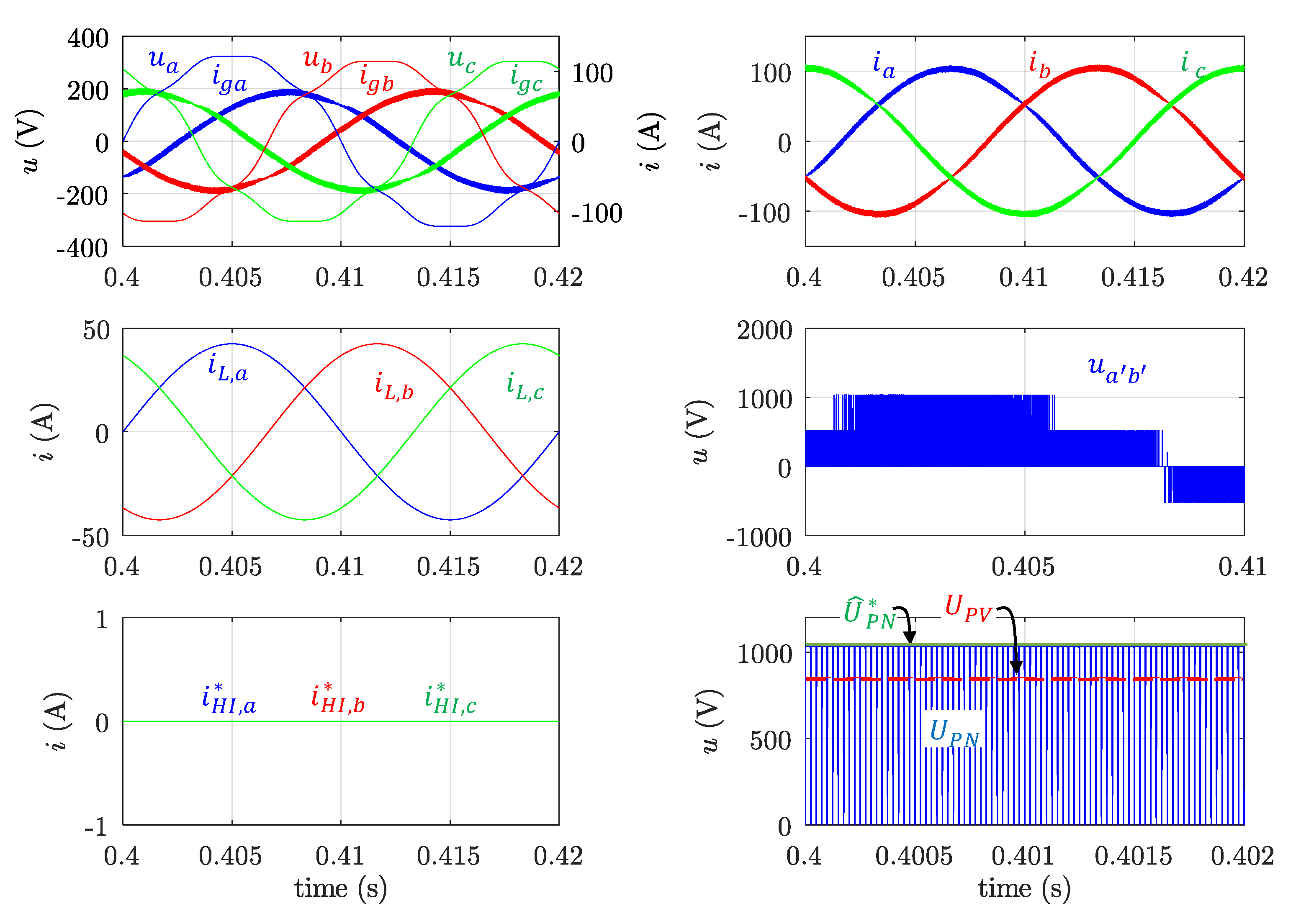
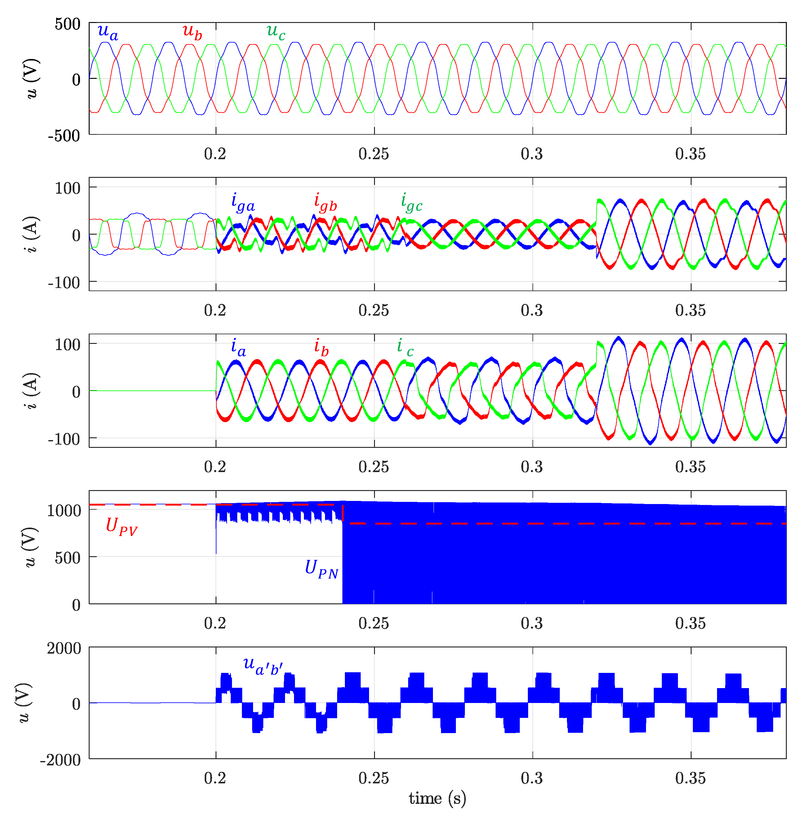
The present study is focused on PVI power range of 50–200 kW, which is suited for commercial and industrial applications and for multi-megawatt PV plants. More specifically, a PVI with the following rating is considered: 230/400 V; 50 Hz, 50 kW. The corresponding rated RMS current I N is 72.5. Table 1 gathers the main equipment parameters. Based on [33,35], the source network components were calculated from the following equations:
C 1 , 4     2 P o u t ( 1 2 D 0 ) U P V 2 f s w K C
C 2 , 3     2 P o u t ( 1 2 D 0 ) D 0 U P V 2 f s w K C ( 1 D 0 )
L 1 , 2 , 3 , 4     U P V ( 1 D 0 ) D 0 2 I P V f s w K L ( 1 2 D 0 )
In these equations, besides the previously defined parameters, f s w is the switching frequency; K L is the assumed ripple in I P V ; P o u t is the rated output power; and K C is the maximum voltage ripple across the capacitors.
The output voltage harmonic distortion at the switching frequency is reduced by means of an output filter constituted by the inductors L f , the values of which are calculated based on [36] from the following equation:
L f     U i n v ( h s w ) · U g 2 π f 1 · h s w · P o u t · T H D I   ,
where U i n v ( h s w ) is the desired harmonic distortion of the output voltage at the switching frequency; U g is the RMS grid voltage (phase-to-neutral); f 1 is the fundamental frequency; h s w is the switching harmonic order; and T H D I is the assumed total harmonic distortion of the output current.
An equivalent load representative of the CIN’s linear and non-linear loads, others than the PVIs themselves, is considered. The rated apparent power demanded by this load is supposed to be close to the total amount of installed PV power in the CIN. This would allow the CIN to operate in off-grid mode. At the PCC, the CIN-EMS measures the CIN’s load current ( i L C I N ) and assigns a fraction ( i L ) to each PVI. According to [37], in commercial buildings and industrial plants, harmonic analysis and the corresponding correction measures are required when a large number of non-linear loads (typically greater than 25% to 30% of the total load) are present or anticipated to be added. Hence, in this work, as a representative example, harmonic and imbalance compensation over about 40% of the CIN’s total demand is proposed. Therefore, the load RMS current allocated to a specific PVI will be approximately 40% of the rated RMS current of the PVI itself, i.e., in this case I L = 30 A.
A simulation model for a PVI, in the conditions described above, has been developed using PSCAD simulation tool. Both the switching frequency and the sampling rate were considered 10 kHz and a simulation time step was taken 10 6 s. The four-wire LV network was supposed to be distorted and unbalanced according to [38,39]. Individual distortion percentage for harmonic 3 is selected at its limit, while for harmonics 5 and 7 the percentages are calculated for having a Total Harmonic Distortion (THD) below the 8% limit. The inverse sequence component ( U ) is set at its limit, adding a zero-sequence component ( U 0 ) fixed at the same value. These values are shown in Table 2.
Simulation results are displayed in Figure 6, Figure 7, Figure 8, Figure 9 and Figure 10. Simulation starts at t = 0 with two different PV voltages values, corresponding to different solar irradiance conditions. The required DC link voltage is set to U ^ P N * = 1060 V. At t = 0.2 s, the three control modes (P, Q, and HI), along with the ST control, are activated. The following cases are considered.
  • Case A. PV voltage set to U P V   = 1060 V. MPPT mode. Injecting active power close to rated power and no reactive power: P * = 50 kW; Q 1 * = 0. CIN load without harmonics nor imbalance.
  • Case B. PV voltage set to U P V = 850 V. RPPT mode. Injecting active and reactive power: P * = 45 kW; Q 1 * = 21.7 kVAr. CIN’s load without harmonics nor imbalance.
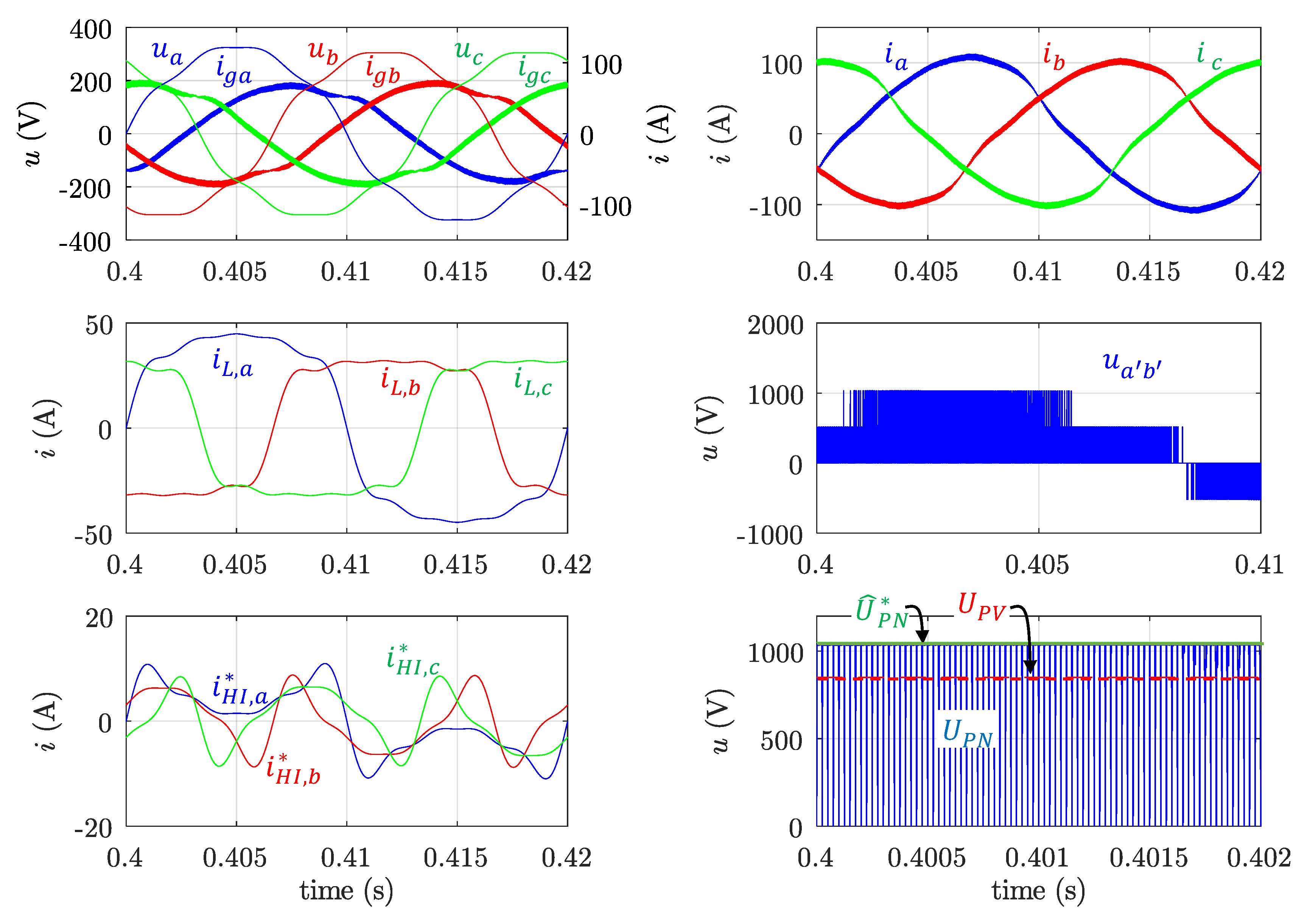
  • Case C. PV voltage set to U P V = 850 V. RPPT mode. Injecting active and reactive power: P * = 45 kW; Q 1   * = 15 kVAr. CIN’s load with odd harmonic currents up to 9th order as the maximum established by the IEC TS 61000-3-4 standard [40]. Harmonic and imbalance content are shown in Table 3. For this load, the RMS value of the equivalent current, calculated according to Std. IEEE-1459:2010 [41] is I L e = 31.53   A . The HI compensation function is not activated.
  • Case D. PV voltage set to U P V = 850 V. RPPT mode. Injecting active and reactive power: P * = 45 kW; Q 1 * = 15 kVAR. Harmonic and unbalanced content of CIN’s load as in case C. The HI compensation function is activated.
  • Case E. PV voltage set to U P V = 850 V. RPPT mode. Injecting active and reactive power: P * = 45 kW; Q 1 * = 21.7 kVAr. Harmonic and unbalanced content of CIN’s load as in cases C and D. The HI compensation function is activated.
The CIN load current is sinusoidal and balanced in cases A (Figure 6) and B (Figure 7), so the reference current for the HI control is null. In case A, no reactive power setpoint is provided by the CIN-EMS, thus only the P control is activated with a reference value imposed by the MPPT algorithm. A unity dPF is attained by the PVI, injecting a current into the grid in phase with the positive-sequence fundamental grid voltage. In case B, the PVI receives active and reactive power setpoints from the CIN-EMS. One can notice that the DC-link voltage is closed to its reference value in both cases. In case A, since the PV voltage is high enough, the boost functionality, by using the ST control, is not needed. In case B, however, it is necessary because the PV voltage is low.
In case C (Figure 8), the CIN load current is distorted (see Table 3) and unbalanced ( I / I + = 10%, I 0 / I + = 10%). Since in this case the HI compensation function is not activated, the grid current is unbalanced and distorted. Table 4 summarizes the harmonic and imbalance components of the load, grid, and PVI phase currents.
In Case D (Figure 9) the CIN load current is distorted and unbalanced as in Case C, however in this case the HI function is activated. The CIN-EMS setpoints and the compensation requirements are compatible with the PVI nominal current, the converter can perform its assigned tasks and therefore balanced sinusoidal grid currents are achieved. Table 5 summarizes the harmonic and imbalance components of the load, grid, and PVI phase currents. As it can be seen, load currents have THD in the range 21-28 %; this figure is notably reduced to below 5% in grid currents. Regarding imbalances, the figures I = 3 A and I 0 = 3 A in the load currents are reduced to 0.14 A and 0.2 A, respectively, in the grid currents.
In Case E (Figure 10), the CIN load current is distorted and unbalanced as in Case C and D, and the HI function is activated. The active power setpoint is 45 kW; however, the reactive power has been increased to 21.7 kVAr. With these values, the compensation requirements cannot be fulfilled without incurring equipment overload. Therefore, the PVI performs a partial compensation and grid currents are not sinusoidal nor balanced. Table 6 summarizes the harmonic and imbalance components of the load, grid, and PVI phase currents for Case E. Paying attention to grid currents, it can be seen that THD is about 7.5% in the worst phase; and I and I 0 are 1.81 and 1.91 A, respectively. These results show the expected saturation effect which ensures the PVI does not exceed its rated RMS current.
Following the definitions proposed in Standard IEEE- 1459:2010 [41], different PVI three-phase power quantities have been calculated. Table 7 summarizes the results for cases A-E. The following power terms are shown: apparent power S in kVA, active power P in kW, fundamental reactive power Q1 in kVAr, non-active power N in kVA, the power factor PF, and the displacement power factor dPF.
Figure 11 demonstrates the behaviour under changing setpoint conditions. The overall performance is described below:
Initially PVI is not connected and consequently the CIN loads are fed solely from the grid; therefore, grid currents are equal to load currents with opposite sign.
At t = 0.2 s, PVI is connected, injecting 30 kW from the PV panels in a specific irradiation condition. At the same time, the Q function is activated to inject fundamental reactive power in the order of one-third of the active power, 10 kVAr in this case. Despite the unbalanced and distorted grid voltage, the PVI output currents waveforms are balanced and sinusoidal, and lagging from the fundamental component of phase voltage. However, since load current is distorted, the currents injected into the grid are unbalanced and distorted.
At t = 0.24 s, PV voltage U P V falls to 850 V; DC-link voltage is regulated to its reference value ( U ^ P N * = 1050   V ), adjusting the ST ratio D 0 . Voltage U P N is zero during ST states and U ^ P N during NST states. These changes are also reflected in u a b .
At t = 0.26 s, HI function is activated, consequently, PVI currents become distorted and unbalanced so the grid currents are sinusoidal and balanced. In this case, total compensation is possible because the PVI rated power is not reached.
At t = 0.32 s, active and reactive power setpoints are increased to P * = 45   kW and Q 1 * = 21.795 kVAr, respectively. In this condition, the equipment performs a partial compensation; consequently, grid currents remain partially distorted and unbalanced.
The implemented model is based on real electrical models with realistic parameters for the power stage. Selected parameters of the IGBTs were obtained from datasheet of 12MBI100VN-120-50 IGBT T-type module by Fuji. Both the transfer functions and the controllers have been implemented in their discrete form using Tustin’s method, and all measurements are sampled before processing at 10 kHz. This gives an insight into the practical feasibility of the proposal using current fast microcontrollers.

4. Conclusions

A control strategy has been presented for photovoltaic converters that allows the control of the overall active and reactive power of the CIN where they are integrated. Additionally, if the converter has spare capacity, the control strategy contributes to reduce the harmonic content and imbalances in the three-phase currents demanded by the entire CIN at the point of connection to the distribution network.
A three-phase Quasi-Z-Source Three-Level T-Type, is used as a grid interactive inverter. This topology has voltage boosting ability and eliminates the requirement for both an additional DC-DC converter and/or a step-up transformer commonly used in PV inverter systems. Therefore, the application of this topology is more efficient than the other conventional two-level and three-level inverter structures for medium frequency operation.
Simulation results have demonstrated that the reference currents can be calculated locally, based on the setpoints received from the CIN-EMS, in a time frame compatible with practical operation, and that these references are correctly followed by the currents supplied by the PVI. Proper operation has been achieved even under distorted and unbalanced LV grid conditions.
No cross-coupling interaction was observed, i.e., active power, reactive power and harmonic-imbalance controls act independently from each other, demonstrating another featured advantage of the proposed global control strategy.
Although the implemented simulation is highly accurate, a laboratory scaled prototype is currently being assembled, in order to experimentally endorse the proposed control strategies on this topology.
The practical use of the proposed PVI systems in CINs will contribute to the smart grid goals, allowing the offer of ancillary services to the distribution system operator and improving the power quality of the LV network.

Author Contributions

Conceptualization, C.R.-C. and F.B.-G.; methodology, E.R.-C. and M.I.M.-M.; software, C.R.-C. and O.H.; validation, M.I.M.-M., E.R.-C. and E.G.-R.; formal analysis, E.R.-C. and F.B.-G.; investigation, F.B.-G., C.R.-C. and O.H.; writing—original draft preparation, C.R.-C. and F.B.-G.; writing—review and editing, M.I.M.-M. and E.G.-R.; supervision, M.I.M.-M. and E.G.-R.; funding acquisition, O.H., E.G.-R. and E.R.-C. All authors have read and agreed to the published version of the manuscript.

Funding

This research was supported by the Spanish Agencia Estatal de Investigación, grant TEC2016-77632-C3-1-R (AEI/FEDER, UE); by Junta de Extremadura, Spain, under the grants GR18087, IB18067 and TA18003. The Estonian Research Council also supported this work, grant PRG675.

Conflicts of Interest

The authors declare no conflict of interest.

References

  1. Teodorescu, R.; Liserre, M.; Rodríguez, P. Grid Converters for Photovoltaic and Wind Power Systems; Wiley: Chichester, UK, 2010; ISBN 9780470057513. [Google Scholar]
  2. Liu, Y.; Abu-Rub, H.; Ge, B.; Blaabjerg, F.; Ellabban, O.; Loh, P.C. Impedance Source Power Electronic Converters; Willey: Chichester, UK, 2016; ISBN 9781119037118. [Google Scholar]
  3. Anderson, J.; Peng, F.Z. Four Quasi-Z-Source Inverters. In Proceedings of the 2008 IEEE Power Electronics Specialists Conference, Rhodes, Greece, 15–19 June 2008; pp. 2743–2749. [Google Scholar]
  4. Schweizer, M.; Friedli, T.; Kolar, J.W. Comparative evaluation of advanced three-phase three-level inverter/converter topologies against two-level systems. IEEE Trans. Ind. Electron. 2013, 60, 5515–5527. [Google Scholar] [CrossRef]
  5. Anthon, A.; Zhang, Z.; Andersen, M.A.E.; Holmes, D.G.; McGrath, B.; Teixeira, C.A. The benefits of SiC mosfets in a T-type inverter for grid-tie applications. IEEE Trans. Power Electron. 2017, 32, 2808–2821. [Google Scholar] [CrossRef] [Green Version]
  6. Husev, O.; Blaabjerg, F.; Roncero-Clemente, C.; Romero-Cadaval, E.; Vinnikov, D.; Siwakoti, Y.P.; Strzelecki, R. Comparison of impedance-source networks for two and multilevel buck–boost inverter applications. IEEE Trans. Power Electron. 2016, 31, 7564–7579. [Google Scholar] [CrossRef]
  7. Ferñao Pires, V.; Cordeiro, A.; Foito, D.; Martins, J.F. Quasi-z-source inverter with a t-type converter in normal and failure mode. IEEE Trans. Power Electron. 2016, 31, 7462–7470. [Google Scholar] [CrossRef]
  8. IEEE Recommended practice and requirements for harmonic control in electric power systems. In IEEE Std 519–2014 (Revision of IEEE Std 519–1992); IEEE: Piscataway, NJ, USA, 2014; pp. 1–29. [CrossRef]
  9. Alfieri, L.; Carpinelli, G.; Bracale, A.; Caramia, P. On the Optimal Management of the Reactive Power in an Industrial Hybrid Microgrid: A Case Study. In Proceedings of the SPEEDAM 2018 International Symposium on Power Electronics, Electrical Drives, Automation and Motion, Amalfi, Italy, 20–22 June 2018; Institute of Electrical and Electronics Engineers Inc.: Piscataway, NJ, USA, 2018; pp. 982–989. [Google Scholar]
  10. Varma, R.K.; Siavashi, E.M. PV-STATCOM: A new smart inverter for voltage control in distribution systems. IEEE Trans. Sustain. Energy 2018, 9, 1681–1691. [Google Scholar] [CrossRef]
  11. Varma, R.K.; Maleki, H. PV solar system sontrol as STATCOM (PV-STATCOM) for power oscillation damping. IEEE Trans. Sustain. Energy 2019, 10, 1793–1803. [Google Scholar] [CrossRef]
  12. Zhang, Y.; Roes, M.G.L.; Hendrix, M.A.M.; Duarte, J.L. Symmetric-component decoupled control of grid-connected inverters for voltage unbalance correction and harmonic compensation. Int. J. Electr. Power Energy Syst. 2020, 115, 105490. [Google Scholar] [CrossRef]
  13. Blaabjerg, F.; Teodorescu, R.; Liserre, M.; Timbus, A.V. Overview of control and grid synchronization for distributed power generation systems. IEEE Trans. Ind. Electron. 2006, 53, 1398–1409. [Google Scholar] [CrossRef] [Green Version]
  14. Rodríguez, P.; Luna, A.; Candela, I.; Mujal, R.; Teodorescu, R.; Blaabjerg, F. Multiresonant frequency-locked loop for grid synchronization of power converters under distorted grid conditions. IEEE Trans. Ind. Electron. 2011, 58, 127–138. [Google Scholar] [CrossRef] [Green Version]
  15. Nian, H.; Shen, Y.; Yang, H.; Quan, Y. Flexible grid connection technique of voltage-source inverter under unbalanced grid conditions based on direct power control. IEEE Trans. Ind. Appl. 2015, 51, 4041–4050. [Google Scholar] [CrossRef]
  16. Zarei, S.F.; Mokhtari, H.; Ghasemi, M.A.; Peyghami, S.; Davari, P.; Blaabjerg, F. Control of grid-following inverters under unbalanced grid conditions. IEEE Trans. Energy Convers. 2020, 35, 184–192. [Google Scholar] [CrossRef]
  17. Santhoshi, B.K.; Sundaram, K.M.; Padmanaban, S.; Holm-Nielsen, J.B.; Prabhakaran, K.K. Critical review of PV grid-tied inverters. Energies 2019, 12, 1921. [Google Scholar] [CrossRef] [Green Version]
  18. Qin, C.; Zhang, C.; Xing, X.; Li, X.; Chen, A.; Zhang, G. Simultaneous common-mode voltage reduction and neutral-point voltage balance scheme for the quasi-z-source three-level t-type inverter. IEEE Trans. Ind. Electron. 2019, 67, 1956–1967. [Google Scholar] [CrossRef]
  19. Jain, S.; Shadmand, M.B.; Balog, R.S. Decoupled active and reactive power predictive control for PV applications using a grid-tied quasi-Z-Source inverter. IEEE J. Emerg. Sel. Top. Power Electron. 2018, 6, 1769–1782. [Google Scholar] [CrossRef]
  20. Khajesalehi, J.; Sheshyekani, K.; Hamzeh, M.; Afjei, E. High-performance hybrid photovoltaic -battery system based on quasi-Z-source inverter: Application in microgrids. Iet. Gener. Transm. Distrib. 2015, 9, 895–902. [Google Scholar] [CrossRef]
  21. Liu, W.; Yang, Y.; Kerekes, T. Characteristic Analysis of the Grid-Connected Impedance-Source Inverter for PV Applications. In Proceedings of the 2019 IEEE 10th International Symposium on Power Electronics for Distributed Generation Systems (PEDG), Xi’an, China, 3–6 June 2019; pp. 874–880. [Google Scholar]
  22. Meraj, M.; Rahman, S.; Iqbal, A.; Ben-Brahim, L.; Alammari, R.; Abu-Rub, H. Virtual Flux Oriented Sensorless Direct Power Control of Qzs Inverter Connected to Grid for Solar Pv Applications. In Proceedings of the IEEE International Conference on Industrial Technology, Melbourne, Australia, 13–15 February 2019; Institute of Electrical and Electronics Engineers Inc.: Piscataway, NJ, USA, 2019; Volume 2019, pp. 1417–1422. [Google Scholar]
  23. Ozdemir, S. Z-source T-type inverter for renewable energy systems with proportional resonant controller. Int. J. Hydrogen Energy 2016, 41, 12591–12602. [Google Scholar] [CrossRef]
  24. Komurcugil, H.; Bayhan, S. PI and Sliding Mode Based Control Strategy for Three-Phase Grid-Tied Three-Level T-Type qZSI. In Proceedings of the IECON 2019.45th Annual Conference of the IEEE Industrial Electronics Society, Lisbon, Portugal, 14–17 October 2019; Volume 1, pp. 5020–5025. [Google Scholar]
  25. Pires, V.F.; Cordeiro, A.; Roncero-Clemente, C.; Martins, J.F. Control Strategy for a Four-Wire T-Type qZSI Based PV System to Support Grids with Unbalanced Non-Linear Loads. In Proceedings of the 2019 IEEE 13th International Conference on Compatibility, Power Electronics and Power Engineering (CPE-POWERENG), Sonderborg, Denmark, 23–25 April 2019; pp. 1–6. [Google Scholar]
  26. Milanes-Montero, M.I.; Barrero-Gonzalez, F.; Pando-Acedo, J.; Gonzalez-Romera, E.; Romero-Cadaval, E.; Moreno-Munoz, A. Smart community electric energy micro-storage systems with active functions. IEEE Trans. Ind. Appl. 2018, 54, 1975–1982. [Google Scholar] [CrossRef]
  27. Low Voltage Electrical Installations. In CENELEC Standards Series HD 60364; International Electrotechnical Commission: Genève, Switzerland, 2016.
  28. Effah, F.B.; Wheeler, P.W.; Watson, A.J.; Clare, J.C. Quasi Z-source NPC inverter for PV application. In Proceedings of the 2017 IEEE PES-IAS PowerAfrica Conference: Harnessing Energy, Information and Communications Technology (ICT) for Affordable Electrification of Africa, PowerAfrica, Accra, Ghana, 27–30 June 2017; pp. 153–158. [Google Scholar]
  29. Milanés-Montero, M.I.; Romero-Cadaval, E.; Barrero-Gonzalez, F. Comparison of control strategies for shunt active power filters in three-phase four-wire systems. IEEE Trans. Power Electron. 2007, 22, 229–236. [Google Scholar] [CrossRef]
  30. Miñambres-Marcos, V.M.; Guerrero-Martínez, M.Á.; Barrero-González, F.; Milanés-Montero, M.I. A grid connected photovoltaic inverter with battery-supercapacitor hybrid energy storage. Sensors 2017, 17, 1856. [Google Scholar] [CrossRef] [PubMed] [Green Version]
  31. Milanés-Montero, M.I.; Romero-Cadaval, E.; Rico De Marcos, A.; Miñambres-Marcos, V.M.; Barrero-González, F. Novel Method for Synchronization to Disturbed Three-Phase and Single-Phase Systems. In Proceedings of the IEEE International Symposium on Industrial Electronics, Vigo, Spain, 4–7 June 2007; pp. 860–865. [Google Scholar]
  32. Roncero-Clemente, C.; Husev, O.; Romero-Cadaval, E.; Martins, J.; Vinnikov, D.; Milanes-Montero, M.I.I. Three-Phase Three-Level Neutral-Point-Clamped QZ Source Inverter with Active Filtering Capabilities. In Proceedings of the 2015 9th International Conference on Compatibility and Power Electronics, CPE 2015, Costa da Caparica, Portugal, 24–26 June 2015; Institute of Electrical and Electronics Engineers Inc.: Piscataway, NJ, USA, 2015; pp. 216–220. [Google Scholar]
  33. Husev, O.; Roncero-Clemente, C.; Romero-Cadaval, E.; Vinnikov, D.; Jalakas, T. Three-level three-phase quasi-Z-source neutral-point-clamped inverter with novel modulation technique for photovoltaic application. Electr. Power Syst. Res. 2016, 130, 10–21. [Google Scholar] [CrossRef]
  34. Qin, C.; Zhang, C.; Chen, A.; Xing, X.; Zhang, G. A space vector modulation scheme of the quasi-z-source three-level t-type inverter for common-mode voltage reduction. IEEE Trans. Ind. Electron. 2018, 65, 8340–8350. [Google Scholar] [CrossRef]
  35. Panfilov, D.; Husev, O.; Khandakji, K.; Blaabjerg, F.; Zakis, J. Comparison of three-phase three-level voltage source inverter with intermediate dc–dc boost converter and quasi-Z-source inverter. IET Power Electron. 2016, 9, 1238–1248. [Google Scholar] [CrossRef]
  36. Husev, O.; Chub, A.; Romero-Cadaval, E.; Roncero-Clemente, C.; Vinnikov, D. Voltage distortion approach for output filter design for off-grid and grid-connected PWM inverters. J. Power Electron. 2015, 15, 278–287. [Google Scholar] [CrossRef] [Green Version]
  37. IEEE Recommended practice for conducting harmonic studies and analysis of industrial and commercial power systems. In IEEE Standard 3002.8-2018; IEEE: Piscataway, NJ, USA, 2018; pp. 1–79.
  38. Voltage characteristics of electricity supplied by public electricity networks. In EN 50160:2010; CENELEC: Brussels, Belgium, 2015.
  39. Electromagnetic compatibility (EMC)-Part 2-2: Environment-Compatibility levels for low-frequency conducted disturbances and signalling in public low-voltage power supply systems. In IEC 61000-2-2: 2002; International Electrotechnical Commission: Genève, Switzerland, 2002.
  40. Electromagnetic compatibility (EMC)-Part 3-4: Limits-Limitation of emission of harmonic currents in low-voltage power supply systems for equipment with rated current greater than 16 A. In IEC TS 61000-3-4:1998; International Electrotechnical Commission: Genève, Switzerland, 1998.
  41. IEEE Standard Definitions for the Measurement of Electric Power Quantities Under Sinusoidal, Nonsinusoidal, Balanced, or Unbalanced Conditions. In IEEE Std 1459-2010 (Revision of IEEE Std 1459-2000); IEEE: Piscataway, NJ, USA, 2010; pp. 1–50.
Figure 1. Photovoltaic (PV) based commercial and industrial nanogrid architecture.
Electronics 09 01233 g001
Figure 2. Three-phase topology for one PV inverter (PVI) and the assigned fraction of the facility’s unbalanced and non-linear loads.
Electronics 09 01233 g002
Figure 3. Block diagram of the PVI control system.
Electronics 09 01233 g003
Figure 4. Block diagram of the current controller and modulator.
Electronics 09 01233 g004
Figure 5. Switching signal generation with the level-shifted Pulse Width Modulation (LS-PWM) in phase disposition with the constant boost control (CBC) scheme.
Electronics 09 01233 g005
Figure 6. Simulation results. Case A. CIN setpoints (sent at t = 0.2 s): P * = 50 kW, Q 1 *   = 0. CIN load without harmonics nor imbalance: I L = 30 A. From left to right and top to bottom: grid voltages ( u a ,   u b ,   u c ) and grid currents ( i g a ,   i g b ,   i g c ) ; PVI output currents ( i a ,   i b ,   i c ) ; load currents ( i L a ,   i L b ,   i L c ) ; phase-to-phase PVI output voltage before filtering ( u a b ); harmonics and imbalance compensation PVI reference currents ( i H I , a * ,   i H I ,   b * ,   i H I , c * ) ; and PV voltage ( U P V ), DC-link voltage ( U P N ) and reference DC-link voltage ( U ^ P N * ).
Electronics 09 01233 g006
Figure 7. Simulation results. Case B. P * = 45 kW, Q 1 * = 21.7 kVAr. CIN load without harmonics. I L = 30 A. From left to right and top to bottom as in Figure 6.
Electronics 09 01233 g007
Figure 8. Simulation results. Case C. P * = 45 kW and Q 1 * = 15 kVAr. CIN load containing harmonic components specified in Table 4. From left to right and top to bottom as in Figure 6.
Electronics 09 01233 g008
Figure 9. Simulation results. Case D. P * = 45 kW and Q 1 * = 15 kVAr. CIN load containing harmonic and unbalanced components specified in Table 3. From left to right and top to bottom as in Figure 6.
Electronics 09 01233 g009
Figure 10. Simulation results. Case E. P * = 45 kW and Q 1 * = 21.7 kVAr. CIN load containing harmonic and unbalanced components as in Case D. From left to right and top to bottom as in Figure 6.
Electronics 09 01233 g010
Figure 11. Behavior under changing setpoint conditions. From top to bottom: grid voltages ( u a ,   u b ,   u c ) ; grid currents ( i g a ,   i g b ,   i g c ) ; PVI output currents ( i a ,   i b ,   i c ) ; PV voltage ( U P V ), DC-link voltage ( U P N ) ; and phase-to-phase PVI output voltage before filtering ( u a b ).
Electronics 09 01233 g011
Table 1. Main parameter values for the 3-phase PVI.
ParameterValueUnit
Inductors L 1 L 4 0.5 mH
Capacitors C 1 C 4 2.2 mF
Output Filter L f 0.75 mH
PV voltage U P V 800 1100 V
Output voltage (phase-to-neutral) U g 230 V
K L and K C 0.05p.u.
U i n v ( h s w ) 0.05p.u.
T H D I 0.05p.u.
Rated output power P o u t 50kW
Table 2. Low Voltage (LV) network characteristics.
Voltage Harmonic Distortion (%)Voltage
THD (%)
U / U + U 0 / U +
HD3HD5HD7(%)(%)
54.547.8322
U + , U , U 0 : positive-, negative- and zero-sequence fundamental components.
Table 3. Harmonic content of the Commercial and Industrial Nanogrids (CIN) current for cases C-E.
Individual Harmonic Distortion
(% Respect to the Positive-Sequence Fundamental Component)
Total Harmonic Distortion
THD (%)
I / I + ( % ) I 0 / I + ( % )
HD3HD5HD7HD9
21.610.77.23.825.441010
I + , I , I 0 : positive-, negative- and zero-sequence fundamental components.
Table 4. Harmonic and imbalance components of load, grid and PVI currents for case C.
CurrentHarmonics Imbalance
I 1   ( A ) I 3   ( A ) I 5   ( A ) I 7   ( A ) I 9   ( A ) I   ( A ) THD (%) I   ( A ) I 0   ( A )
i L a 366.483.212.161.1436.8021.2033
i L b 276.483.212.161.1428.0628.27
i L c 276.483.212.161.1428.0628.27
i g a 37.597.023.662.541.1638.5622.923.263.19
i g b 45.196.883.622.561.1445.9718.79
i g c 45.256.843.592.531.1646.0318.65
i a 68.590.540.450.380.0268.613.040.260.19
i b 69.210.410.410.400.0169.233.00
i c 69.250.360.380.370.0469.272.97
I 1 I 9 : RMS harmonic components; I : RMS total. I , I 0 : negative- and zero-sequence RMS fundamental component.
Table 5. Harmonic and imbalance components of load, network and PVI currents for case D.
CurrentHarmonics Imbalance
I 1   ( A ) I 3   ( A ) I 5   ( A ) I 7   ( A ) I 9   ( A ) I   ( A ) THD (%) I   ( A ) I 0   ( A )
i L a 366.483.212.161.1436.8021.2033
i L b 276.483.212.161.1428.0628.27
i L c 276.483.212.161.1428.0628.27
i g a 42.890.320.150.150.2042.934.600.140.20
i g b 42.390.410.150.180.2142.434.80
i g c 42.470.460.150.210.1842.514.82
i a 74.966.723.172.101.2975.3910.753.133.20
i b 66.046.883.202.051.3166.5412.43
i c 66.106.883.182.061.2866.6012.41
Table 6. Harmonic and imbalance components of load, network and PVI currents for case E.
CurrentHarmonics Imbalance
I 1   ( A ) I 3   ( A ) I 5   ( A ) I 7   ( A ) I 9   ( A ) I   ( A ) THD (%) I   ( A ) I 0   ( A )
i L a 366.483.212.161.1436.8021.2033
i L b 276.483.212.161.1428.0628.27
i L c 276.483.212.161.1428.0628.27
i g a 48.322.511.410.980.4148.457.491.191.09
i g b 50.502.351.341.030.3650.626.95
i g c 50.562.371.421.090.3950.687.07
i a 76.913.971.801.180.7577.066.461.811.91
i b 71.974.131.891.140.7972.157.13
i c 71.984.121.791.080.7672.157.05
Table 7. Power terms according to IEEE-1459:2010.
CasesS (kVA)P (kW) Q 1 (kVAr) N (kVA)PFdPF
A 50.4850.090.7576.280.990.99
B 51.0344.1325.0725.620.860.87
C 47.8644.2217.5518.300.920.93
D 49.1344.7317.5420.250.910.93
E 51.4544.4025.0826.000.860.87

