1. Introduction
The huge amounts of data generated from latest and future high-resolution, high-speed imagers in Earth Observation (EO) satellite missions, make image data compression one of the most challenging on-board payload data processing tasks. In 2005, the Consultative Committee for Space Data Systems (CCSDS) issued the Image Data Compression (IDC) standard CCSDS 122.0-B.1 [
1]. CCSDS-IDC defines a particular transform-based image data compression algorithm applicable to many types of spaceborne instrument payloads. The recommended standard provides both lossless and lossy (both rate and quality limited) compression, suitable for monoband two-dimensional (2D) images. When compared to the JPEG2000 reference standard for 2D image compression for consumer applications, the CCSDS-IDC recommended standard has lower complexity since it was designed specifically targeting space applications and space systems design under Size, Weight, Power and Cost (SWaP-C) constraints. Both algorithms, rely on progressive Bit-Plane Encoding (BPE) of Discrete Wavelet Transformed (DWT) image data, both providing a choice of integer and a floating-point DWT so that effective lossless and lossy compression can be achieved, respectively. JPEG2000 offers better compression effectiveness but has higher implementation complexity. Focusing on the DWT, the CCSDS-IDC recommended floating-point DWT is the same 9/7 float as the one included in the JPEG2000. However, the CCSDS-IDC integer DWT is a 9/7M DWT while the JPEG2000 is a 5/3 DWT. Although the 5/3 integer DWT has low complexity and provides excellent lossless compression effectiveness, in tests performed by the CCSDS Multispectral Hyperspectral Data Compression (SLS-MHDC) Working Group (WG) during the development of CCSDS-IDC, the 9/7M integer DWT showed better rate-distortion performance than the 5/3 integer DWT, when other parts of the compression algorithm are fixed. Moreover, in terms of lossless compression performance, the 9/7 integer DWT also performs better according to similar tests. This motivated the CCSDS SLS-MHDC WG to consider two 9/7 integer DWTs, referred to as “9/7F” and “9/7M” following the terminology of [
2]. Comparing between the 9/7M and 9/7F filters, the 9/7M provides better compression performance, especially for lossless compression and at high bitrates. The analysis of the computational complexity between the 5/3, the 9/7M and the 9/7F filters [
2] using the lifting scheme, shows that the 5/3 filter has the lowest complexity (5 additions, 2 shifts, 0 multiplications). The 9/7M filter has moderately higher complexity than the 5/3 filter (9 additions, 3 shifts, 0 multiplications) while the 9/7F filter has significantly higher complexity (26 additions, 18 shifts, 0 multiplications). For these reasons, the 9/7M filter was considered by the CCSDS SLS-MHDC WG as the best trade-off in terms of complexity and compression performance and was selected as the integer DWT for the CCSDS-IDC recommended standard. Recently, CCSDS updated the CCSDS-IDC recommended standard [
3]. The Issue 2 adds modifications to support the Recommended Standard for Spectral Preprocessing Transform for Multispectral and Hyperspectral Image Compression [
4]. It supports images with higher dynamic ranges and larger output word sizes (up to 64-bit words).
Application-Specific Integrated Circuits (ASICs) are designed to be optimum for a particular application. Therefore, ASICs for on-board image compression can achieve high performance and low power. There are two ASIC implementations of the 9/7M DWT. An ASIC was developed by Univ. of Idaho and NASA/GSFC in 0.25 um radiation hardened by design (RHDB) technology to implement the CCSDS-IDC DWT [
5]. The ASIC is fully immune to Single Event Latch-up (SEL) up to 120 MeV-cm
/mg and Single Event Upset (SEU) up to 55 MeV-cm
/mg and achieves a maximum throughput of 20 MSamples/sec at a clock frequency of 100 MHz. The power consumption is 163 mW/MSample and thus requires about 3.3 Watts for the maximum throughput. The CCSDS Wavelet Image COMpression ASIC (CWICOM) [
6] developed by Astrium in the framework of an ESA contract is implemented in a radiation tolerant technology (ATMEL ATC18RHA) with internal EDAC, can tolerate Total Ionizing Dose (TID) up to 100 Krad, implements CCSDS-122.0-B.1 and achieves a maximum throughput of 60 MSamples/sec at a clock frequency of 60 MHz. The power consumption is about 100 mW/MSample and thus requires about 6 Watts for the maximum throughput.
Current SRAM FPGA technology offers qualification for space applications, high density, and dynamic partial reconfiguration for in-flight adaptability and time–space partitioning of on-board data processing tasks. Such FPGA technology offers unique advantages over both one-time programmable FPGAs and ASICs and can be considered an excellent platform for implementation of on-board payload data processing due to its ability to support upgrades after launch, greatly enhancing mission profile and extending valuable system lifetime. The Xilinx 65 nm Virtex-5QV SRAM FPGA, currently in use in several space missions and U.S. classified programs, offers RHBD, high density and dynamic partial reconfiguration. Although Virtex-5QV (XQR5VFX130) is a mature product in stable production accumulating heritage since 2014, recently (May 2020), Xilinx announced the launch of the next generation of Radiation Tolerant (RT) space-grade FPGA technology, the 20 nm Kintex Ultrascale XQRKU060 SRAM FPGA. Having performed well in Single Event Effect (SEE) testing and with no identified need for additional RHBD modifications, with no SEL susceptibility seen up to 79.2 MeV-cm/mg and good TID test performance up to 100Krad, the Kintex UltraScale device is expected to achieve QML Class Y certification in September 2020.
There are a few existing space-grade FPGA implementations of the 9/7M DWT. In the CCSDS-IDC implementation of [
7], the proposed DWT architecture achieves 1.33 cycles/sample. When targeting the Virtex-5QV FPGA, it achieves 136 MSamples/sec at a clock frequency of 191 MHz. When targeting a Kintex 7 (7k325t-ffg676) FPGA, it achieves 227 MSamples/sec at a clock frequency of 318 MHz. In the CCSDS-IDC implementation of [
8], the proposed DWT architecture processes 2 samples/cycle and when targeting the Virtex-5QV FPGA, it achieves 200 MSamples/sec at a clock frequency of 100 MHz. In the CCSDS-IDC implementation of [
9] for the Formosat-5 mission, the proposed DWT architecture when targeting the Virtex-5QV FPGA, achieves 40.4 MSamples/sec at a clock frequency of 45 MHz.
In this paper, we introduce a high-performance architecture for the 9/7M DWT of the CCSDS-IDC algorithm. The proposed parallel architecture achieves 2 samples/cycle while the very deep pipeline enables very high clock frequencies. Moreover, it exploits elastic pipeline principles to provide modularity, latency insensitivity and distributed control. The implementation of the proposed architecture on a Xilinx Kintex Ultrascale XQRKU060 space-grade SRAM FPGA achieves state-of-the-art throughput performance of 831 Msamples/s (13.3 Gbps @ 16bpp) and outperfoming previous implementations on the same reference FPGA technology (Virtex-5QV). Such a high-performance implementation allows seamless integration with next-generation high-speed imagers and on-board data handling networking technology (i.e., SpaceFibre high-speed serial link).
The paper is organized as follows: In
Section 2, a brief description of the CCSDS-IDC algorithm is presented along with the focus of this paper, the 9/7M integer DWT. In
Section 3, the proposed architecture for the 9/7M Integer DWT is introduced. The verification and validation strategy of the 9/7M Integer DWT design is described in
Section 4. Experimental implementation results and comparisons are provided in
Section 5, while
Section 6 concludes the paper.
3. Proposed Architecture
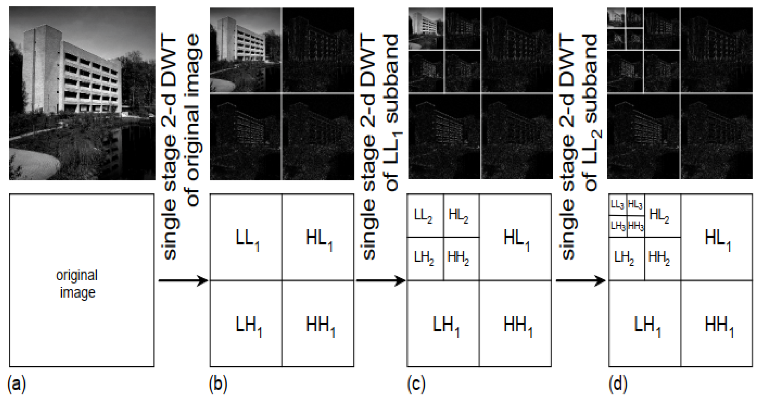
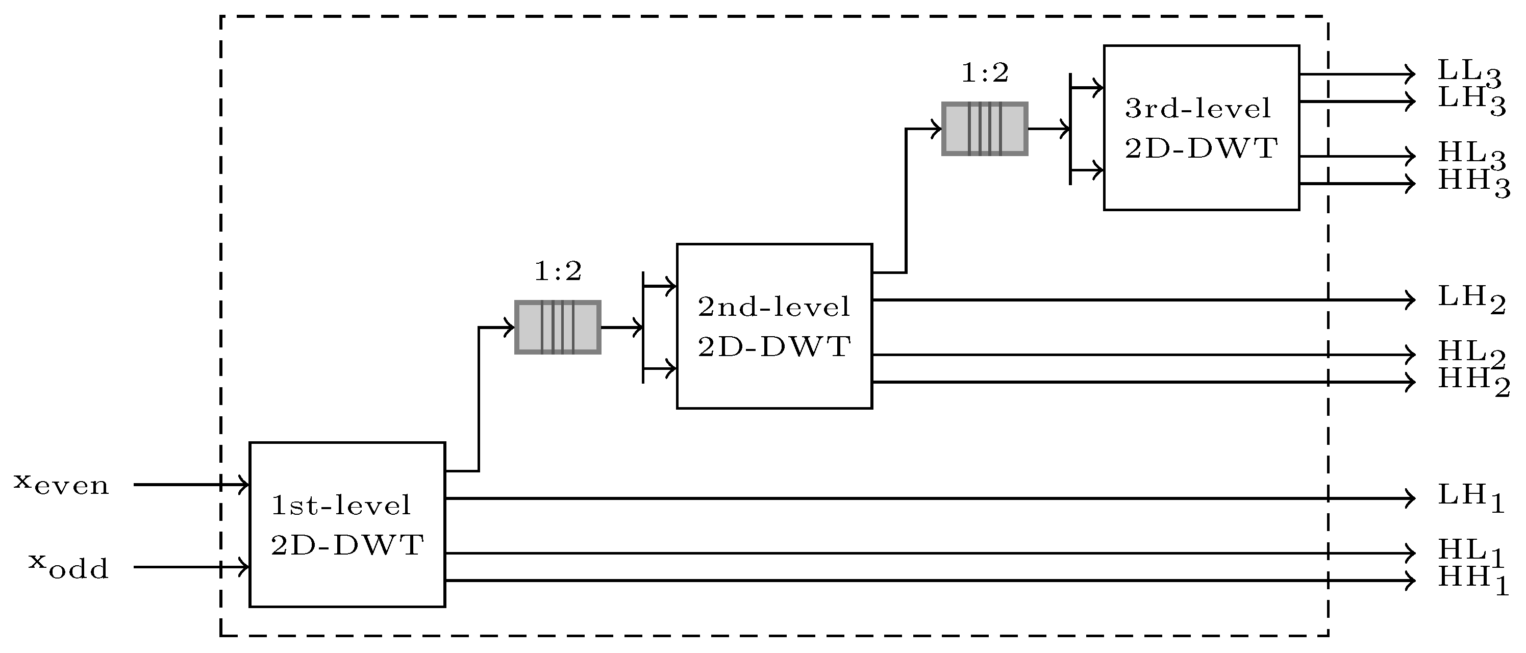
The proposed architecture is a line-based DWT architecture which enables a single FPGA chip solution without any external memory requirements. The top-level architecture of the proposed 3-level 2D-DWT is shown in
Figure 5. The DWT unit receives two consecutive pixels (odd and even) in parallel and performs three levels of 2D-DWT producing 10 sub-bands. In the proposed streaming architecture, all three cascaded levels of 2D-DWT are operating in parallel, independently of each other, in an elastic pipeline with distributed control to handle back-pressure, with the LL sub-band of each level driving the next level. The independent 2D-DWT computational modules in the elastic pipeline are decoupled with full throughput using small FIFOs. Internally to the 2D-DWT, elasticity is provided using Elastic Buffers (ELBs) between sub-units, also at full throughput. To increase the reusability, testing and ease of maintenance of sub-units, a modular architecture is considered. Towards this direction, the same 2D-DWT VHDL design was reused in all three levels using VHDL generics to configure the different memory sizes required. The 2D-DWT unit is designed to receive two pixels per cycle. This is essential for the first level; however, asymmetric (“gearbox”) decoupling FIFOs with ratio 1:2 are required between the two subsequent levels.
The input pixels are expected to enter the 3-level 2D-DWT unit in a raster-scan pixel order using an AXI4-Stream compatible interface. The proposed architecture provides flexibility supporting both frame images (produced by CCD array type sensors) and strip-based images (produced by push-broom type sensors). The maximum image width (number of columns) is statically (at compile time) configurable using VHDL generics. The input interface towards the sensor ReadOut Electronics requires end-of-line (EOL) and end-of-stream (EOS) signals accompanying the input data stream. Note that it is easy to provide an external wrapper to generate these ’EOL’ and ’EOS’ signals based on statically (at compile time) or dynamically (at run-time) configured image dimensions (width and height). An ’EOS’ signal is also propagated to the ten sub-band output streams of the 3-level 2D-DWT unit to ease the integration of the proposed DWT design at system-level for a CCSDS-IDC implementation. The ten sub-band outputs are also using an AXI4-Stream interface. In the following subsections, a detailed description of each of the sub-units is provided.
3.1. Architecture of the 2D-DWT Unit
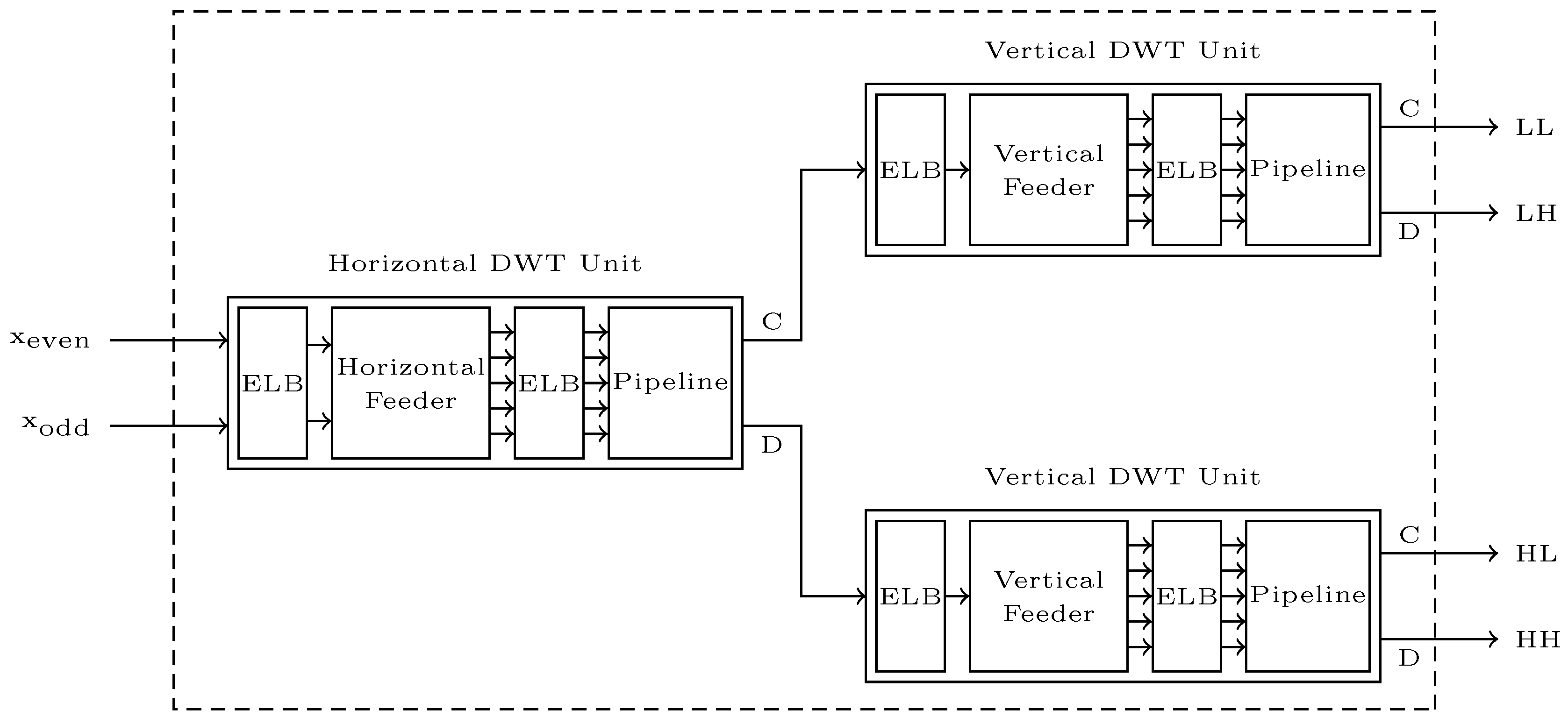
Each 2D-DWT unit consists of one Horizontal and two Vertical DWT units, as seen in
Figure 6.
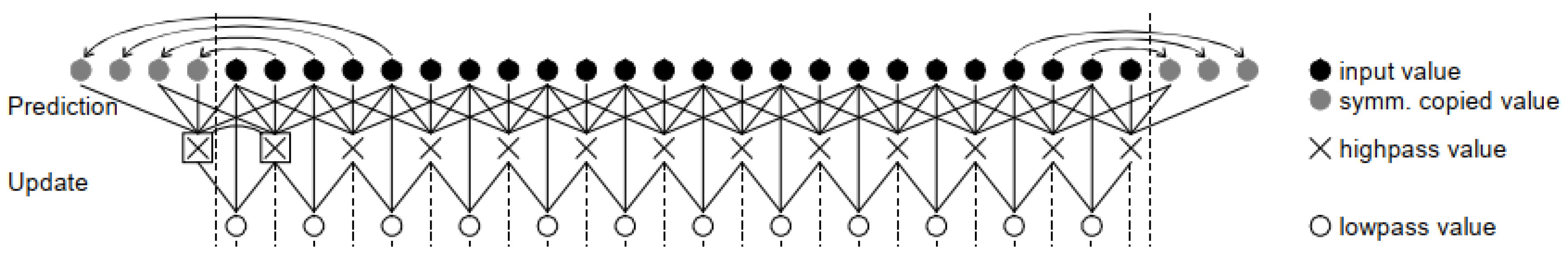
These units also have modular architecture using a common arithmetic pipeline design, since they perform the same 9/7M DWT. However, Horizontal and Vertical DWT units differ in the way they rearrange the incoming data so that the proper 5-tuples of pixels/coefficients (, , , , ) enter the arithmetic pipeline. In particular, the Horizontal DWT unit performs the DWT operation on neighbor pixels/coefficients of the same input line, while the Vertical DWT performs the DWT operation on pixels/coefficients residing in the same column relating to the five previous input rows. The unit that generates the proper 5-tuples out of the input stream is called a ’Feeder’ (Horizontal or Vertical), as it feeds the right data into the arithmetic Pipeline unit.
Concerning the DWT operation, the input to the level 2D-DWT unit are data rows from the kth LL sub-band . A row from this sub-band has width equal to pixels where is the maximum number of columns of the input image. The output of the 2D-DWT are data rows of four sub-bands at level : , , , , where the index denotes the level of the dyadic decomposition and denotes the input image. The Horizontal DWT unit splits each input into a low-pass and a high-pass stream. Each of these two streams is then passed to the Vertical DWT unit, producing the final , , and sub-band streams. Both Horizontal and Vertical DWT units produce coefficients as soon as the corresponding input data become available in a streaming pipeline.
The proposed architecture results in low memory requirements, as the DWT units only have to store and update input data needed for calculating the current output high-pass and low-pass coefficients. It should be noted that the memory requirements are dominated by the Vertical DWT unit where seven rows are buffered on-chip. The memory requirements depend solely on the maximum image width and not on the total image size (independent of the image height) making the architecture suitable for push-broom imagers.
Finally, Elastic Buffers (ELBs) have been used between sub-units, as seen in
Figure 6, to improve system timing closure and provide decoupling of independent computational pipelines of the proposed streaming architecture.
3.2. Horizontal DWT Unit
The Horizontal DWT unit is depicted in
Figure 6. It has also a modular architecture, and it is composed of two sub-units, each with its own controller: a Horizontal Feeder and an arithmetic Pipeline. The two sub-units are communicating using ELBs. Each of these two sub-units is described in this section.
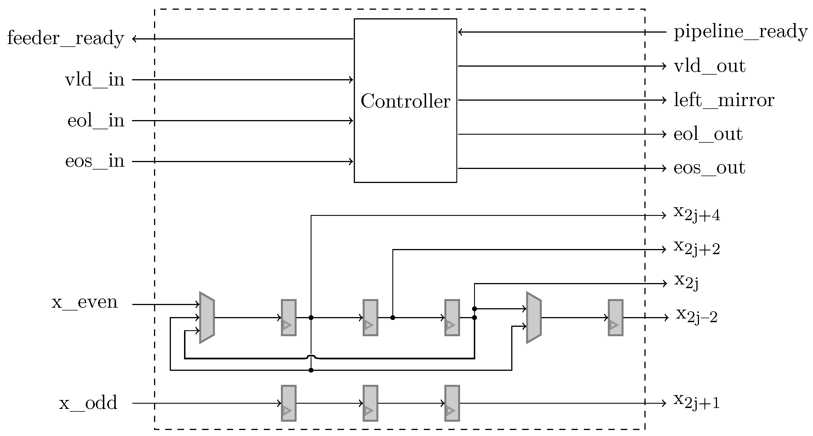
The Horizontal Feeder is depicted in
Figure 7. It receives 2 input pixels (in the 1st DWT level) or coefficients (for subsequent DWT levels) in parallel (
,
) and produces a valid 5-tuple to be used by the arithmetic pipeline for calculating the high-pass
and low-pass
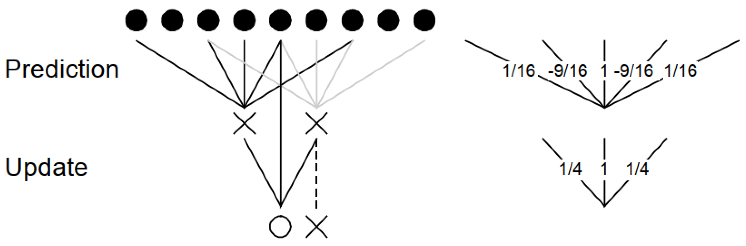
coefficients. Since the Horizontal DWT processes the inputs sequentially, the filter taps are implemented on FPGA slice registers. Additionally, this unit takes care of the special mirroring conditions, specified in the recommended 9/7M DWT (see Equations (
1)), by multiplexing specific slice-register-based filter taps.
The Pipeline unit implements the arithmetic pipeline of the recommended 9/7M DWT. It receives the proper 5-tuples by the Feeder unit and calculates the high-pass
and low-pass
coefficients. Eight pipeline stages were required to achieve timing closure for the targeted frequency. The datapath of the Pipeline unit is shown in
Figure 8.
The modularity of the proposed architecture enables sharing the arithmetic pipeline design by both horizontal and vertical units since they perform the same 9/7M DWT. The calculation of each low-pass coefficient
of the DWT, requires both current
and its previous
high-pass coefficients. However,
is different for horizontal and vertical units, and in particular, in the Horizontal DWT unit is the previous one computed, while in the Vertical DWT unit it is the one computed one line (of width
w) earlier. This
coefficient is depicted in
Figure 8 in pipeline stage 5 using the
configurable delay symbol. The delay is configured statically at compile time using a VHDL generic which dictates whether a simple register (
w=1) or a FIFO with depth equal to the line width
w is instantiated, depending on whether the arithmetic pipeline is meant to be used in a horizontal unit or in a vertical one respectively. Furthermore, in order to calculate the first low-pass coefficient
, along with the
coefficient, a specific ’left_mirror’ control signal is required that accompanies the input 5-tuples which is set to ’1’ by the corresponding Horizontal or Vertical Feeder for the 5-tuples corresponding to the first low-pass coefficient
calculation, for 1 cycle or for line-width cycles, respectively. This ’left_mirror’ control signal informs the arithmetic pipeline’s controller how to produce the select signal of the multiplexer after the
element as seen in
Figure 8 in pipeline stage 5. The computational complexity of the proposed implementation of the datapath of the arithmetic pipeline unit is 9 additions, 3 shifts and 0 multiplications which is in accordance with the 9/7M algorithm specifications.
3.3. Vertical DWT Unit
The Vertical DWT unit, also depicted in
Figure 6, is instantiated two times in the 2D-DWT unit. It uses the same arithmetic Pipeline unit as the Horizontal DWT unit; however, a different Feeder unit is required.
The Vertical Feeder is more complicated than the Horizontal Feeder since the Vertical DWT processes the input rows in parallel. The five input rows required for the Vertical DWT calculation are buffered in BlockRAM-based FIFOs. The Vertical Feeder is depicted in
Figure 9. The proposed architecture uses a total of seven FIFOs with depth equal to
pixels where
is the maximum number of columns of the input image. As with the Horizontal Feeder, the vertical one takes care of the special mirroring conditions, specified in the recommended 9/7M DWT (see Equation (
1)), by multiplexing specific FIFO-based filter taps.
3.4. Throughput of the Proposed 9/7M DWT
The throughput performance of the proposed 3-level 2-D 9/7M DWT architecture is calculated using Equation (
3).
In Equation (
3),
width and
height refer to the width and height of the image in pixels and
F is the achievable clock frequency in MHz. The variable
total_cycles in the denominator of Equation (
3) is the total number of cycles required to perform the DWT operation while considering no stalls from the 9/7M DWT source (considered always valid) and sink (considered always ready) and it can be calculated using the following equation:
In Equation (
4), the first term,
, denotes the number of cycles required for the total number of image pixels to enter the DWT considering receiving two pixels per cycle. The second term,
, denotes the additional two cycles per row for the mirroring operation of the 1st level horizontal DWT. The third term, +4, denotes the additional 4 cycles needed for the mirroring operation of the 2nd and 3rd level horizontal DWT units (2 cycles each). The fourth term
denotes the additional 4 cycles per column for the mirroring operation of the
columns of the 1st level vertical DWT. The fifth term
denotes the additional 4 cycles per column for the mirroring operation of the
columns of the 2nd level vertical DWT. The sixth term
denotes the additional 4 cycles per column for the mirroring operation of
columns of the 3rd level vertical DWT. All these stall cycles due to mirroring must be added, since for one unit to start its mirroring operation, the previous one in the cascade must have finished its own mirroring operation. The last term in Equation (
4) denotes the total latency of the six levels of arithmetic pipelines (two levels per 2D-DWT), the latency of the two asymmetric (“gearbox”) decoupling FIFOs between the levels of 2D-DWT and the latency of the ELBs between the sub-units of each 2D-DWT for a total of 79 cycles. The total number of cycles can be written as in Equation (
5).
Thus, replacing the
total_cycles in the denominator of Equation (
3), the throughput can be calculated as in Equation (
6).
For large images (large values of
and
) or for images produced by push-broom sensors, the fraction term in Equation (
6) which denotes the samples/cycle is close to 2 samples/cycle.
3.5. Memory Storage Requirements
The memory storage requirements of the proposed architecture are dominated by the Vertical DWT unit where seven rows must be buffered in seven BlockRAM-based FIFOs hosted in the Vertical Feeder sub-unit. Furthermore, one BlockRAM-based FIFO is also required in the arithmetic pipeline of the Vertical DWT unit to store the row of
coefficients. Thus, eight BlockRAM-based FIFOs are required in each Vertical DWT unit and 16 BRAMs-based FIFOs are required in each of the three 2D-DWT units in cascade. The data width of these FIFOs is 20-bits considering the dynamic range expansion of the integer DWT operation from the 16-bit dynamic range of input data [
10]. The depth of the FIFOs is configured to accommodate a row. The width of the row depends on the level
k of the dyadic decomposition being
pixels where
is the number of columns of the input image. Thus, the FIFO depth is
for the two vertical units of the 1st level,
for the two vertical units of the 2nd level and
for the two vertical units of the 3rd level.
The memory storage requirements in terms of BlockRAM use is given in Equation (
7).
For example, considering a maximum width of 4096 pixels (this is statically configured at compile time using a VHDL generic) the memory storage requirements are 1146880 bits.
4. 9/7M DWT Verification and Validation Strategy
The 9/7M DWT VHDL design has been extensively verified by RTL simulation using Mentor Graphics Questa. The tests performed include a significant amount of test images from the corpus of images [
10] available in [
11], the artificial test pattern image of
pixels that was explicitly designed for testing DWT implementations producing maximum dynamic range expansion in all the sub-bands after DWT processing and a significant amount series of random test images. The UNL software implementation in C [
12] was used as a golden reference model of 9/7M DWT.
The testing framework is based on VUnit [
13] and a set of python scripts, as well as the C golden model of the compressor [
12]. Each test campaign is described as a .CSV file with a test on each line and all the static (at compile time) parameters (VHDL generics). Python scripts read the .CSV file and interpret the parameters to invoke the golden compressor binary to produce the verification data. Then a testbench instrumented with VUnit is invoked with the Questa simulator comparing with golden data.
The 9/7M DWT design has been also validated on-chip. The validation platform was a Zynq-7020 SoC FPGA hosted in a ZedBoard development board by Digilent. The XC7Z020 SoC consists of an integrated processing system (PS) and programmable logic (PL), on a single die. The test architecture was based on the principles of pseudorandom testing where test data images were applied by linear-feedback shift registers (LFSRs) to the 9/7M DWT Design Under Test (DUT) and test responses (ten DWT sub-bands) were compacted by multiple-input-signature-registers (MISRs). The ARM-based PS running bare-metal software was the test controller, responsible for the configuration of the LFSR seed and the monitoring and checking of the ten MISR signatures using AXI4-Lite interface. Moreover, the ARM-based PS was communicating with a host-PC via a UART interface. The user of the host-PC provided several test configurations including different image dimensions and LFSR seeds to the ARM processor test controller. A custom hardware test wrapper was designed to provide the 9/7M DWT design with the LFSR pseudorandom data using the AXI4-Stream interface along with the necessary side-channel control EOL and EOS signals. An extensive on-chip test campaign applied several thousands of successful pseudorandom tests.
5. Experimental Results
The proposed architecture was implemented targeting the XCKU060-1FFVA1617l pin compatible commercial equivalent of the upcoming XQRKU060 space-grade FPGA. The throughput performance goal for the XCKU060 device was higher than 800 MSamples/sec for a single instance of the DWT being a direct requirement from a major European space industry prime for next-generation on-board compression modules. Moreover, experimental results are also provided for comparisons with other work targeting the space-grade Virtex-5QV (XQR5VFX130) FPGA. The Xilinx Vivado Design Suite and the ISE Design Suite tools were used for the implementation targeting the XCKU060 and the V5FX130 devices, respectively.
The frequency of 416.7 MHz (period 2.4 ns) was achieved for the maximum image width configuration considered (4096 pixels) although higher clock frequencies were possible for smaller image widths than 4096. The proposed architecture processes 2 samples/cycle and thus the guaranteed throughput performance is higher than 815 MSamples/sec for all image dimensions considered. The throughput performance for the
image is 831 MSamples/sec (13.3 Gbps @ 16 bpp). The detailed implementation statistics including FPGA resources and Static Timing Analysis after Place and Route, for different image dimension configurations are shown in
Table 1.
The available LUTs and BRAMs in the XCKU060 are 331680 and 1080, respectively. Thus, the LUT and BRAM use is less than 2.56% and 4.81%, respectively, for maximum image line-width equal to 4096 pixels. The negligible differences in samples/cycle is due to the Horizontal and Vertical DWT mirroring stalls and the deep pipeline latency. The power consumption statistics were evaluated using the Xilinx Vivado power estimator on the post Place and Route design using default environmental settings. Comparison with other work targeting the same space-grade V5QV (XQR5VFX130) FPGA is shown in
Table 2.
The proposed 9/7M DWT architecture when implemented targeting the V5QV FPGA achieves a maximum frequency of 256 MHz (period 3.9 ns). Considering the 1.995 samples/cycle achieved for an image width of 4096 pixels, it achieves a throughput of 511 MSamples/s (8.17 Gbps @ 16 bpp). This throughput compares favorably with the implementation of [
8], which is the current state-of-the-art also providing with 2 samples/cycle. The proposed architecture sets a new state-of-the-art in throughput performance (speedup of 2.55 targeting the same V5QV FPGA technology), while the FPGA resources are kept as low as possible.


