1. Introduction
Compared with the traditional air insulated switchgear (AIS) substations, gas insulated switchgear (GIS) substations have many advantages such as less occupied space, safe operation, and easy maintenance. In order to improve the intelligence level of GIS substations, intelligent electronic devices (IEDs) are being extensively applied in GIS substations [
1,
2]. The electronic transformer is one part of IEDs, and it is the most critical metering device in GIS substations. As the State Grid Corporation vigorously develops the construction of smart GIS substations, the electronic transformer has become widely used in smart grids due to advantages such as small size, light weight, simple insulation structure, low cost, high measurement accuracy, wide frequency response range, etc.
The International Electrotechnical Commission (IEC) formulated corresponding standards early in 2002, which clearly defined the technical specifications of electronic transformers [
3,
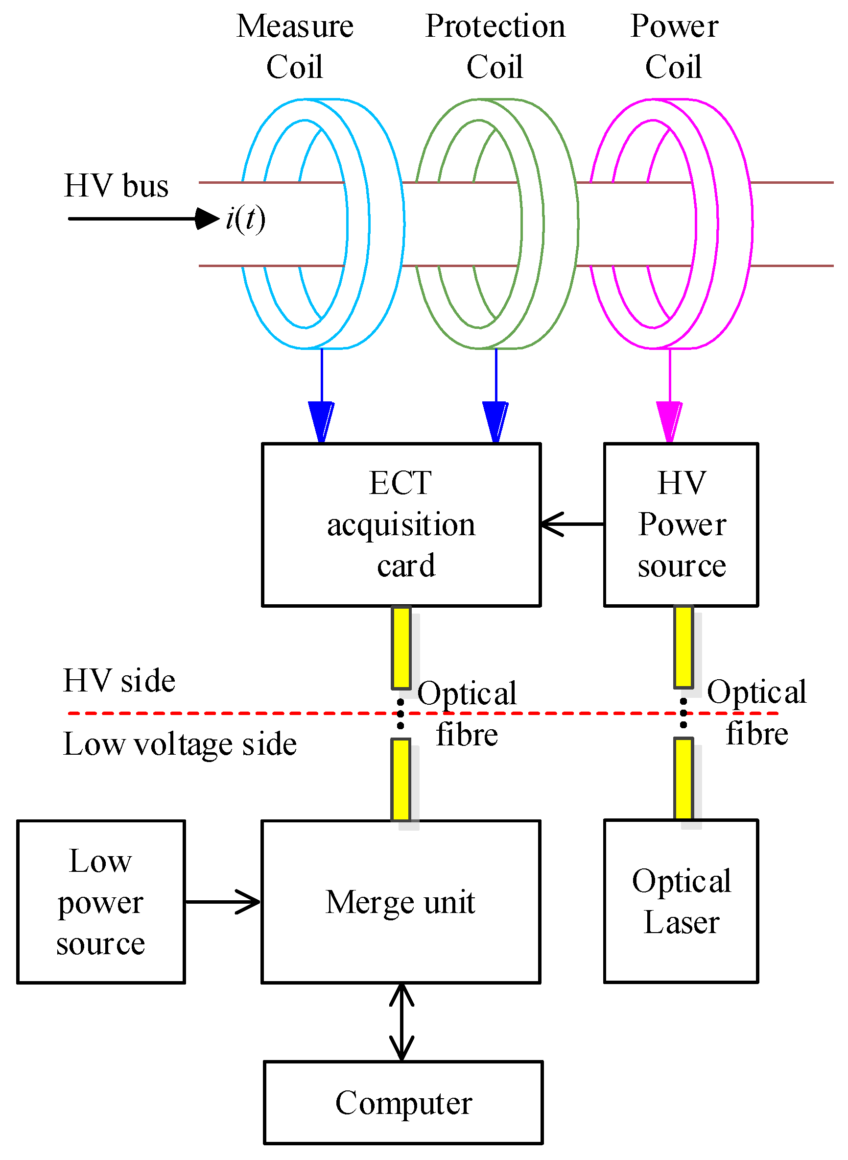
4]. According to the IEC 60044-7 and IEC 60044-8, electronic transformers can be divided into electronic voltage transformers (EVTs) and electronic current transformers (ECTs). The biggest difference between the ECT and EVT is the high voltage (HV) side sensor. Take the ECT as an example: the signal acquisition system of the ECT in a substation is shown in
Figure 1.
As shown in
Figure 1, in the signal acquisition system, the HV power source is the power supply of the ECT acquisition card. The low power source brings energy to the merge unit. The optical laser provides optical signals for the optical fiber. The function of the merge unit (MU) is to receive and process data. The MU can convert the optical signal into analog signals, and then finally transmit the measured HV bus signal to the host computer.
In the practical application of the ECT, lightning strikes and other natural interference sources will impact the low voltage IED [
5]. Besides, the circuit breaker (CB) turn-on or turn-off transient in GIS substations will cause an operating overvoltage with a steep wave head, which contains electromagnetic energy of mutative frequencies. This electromagnetic interference (EMI) is also called very fast transient overvoltage (VFTO) in the electrical power industry [
6]. As shown in
Figure 1, the ECT acquisition card is localized near the HV bus at the HV side. Electromagnetic interference (EMI) issues such as VFTO or lightning strikes in GIS substations are becoming an important factor for the reliability of ECTs [
7,
8]. In order to reduce the influence of these EMIs, the stability and reliability of ECTs or IEDs need to be further improved.
Some research has been performed to study the EMI of IEDs. Parvis presented a fast filtering algorithm and built a precompliance test-set for the measurement of conducted emissions (CE) [
9]. Medico and his team raised a novel machine learning-based approach for error detection, which only requires the raw output data from a susceptibility test [
10]. Ker proposed a modified power-rail ESD clamp circuit, which can provide high enough chip-level ESD robustness, and without suffering the latchup-like failure during the system-level ESD test [
11]. Cerri built a model to describe the electromagnetic (EM) radiation; its experimental validation showed the interfering field can be particularly dangerous for digital circuit functions [
12]. Ayed studied an analog-to-digital converter (ADC) via a probe injecting resistive radio frequency (RF). Then, it was exploited to construct an immunity model of the ADC according to the integrated circuits immunity model-conducted immunity (ICIMCI) model [
13]. Mao and his team analyzed the EMI in a low voltage secondary cable, which was caused by a short circuit fault. Coupling paths through the current transformer and grounding system would destroy the control system and lead to secondary apparatus damage [
14].
Concerning the immunity mechanism, some scholars have already researched how the electrical devices are disturbed [
13,
15,
16,
17]. Richelli reported on an amplifier exhibiting both intrinsic robustness to interferences and presented the successful design of a CMOS operational amplifier (opamp) with enhanced immunity to EMI. Then, he addressed a new approach to design a CMOS opamp which provides a good tradeoff between a high gain and strong immunity to EMI [
18,
19,
20]. Koohestani, based on dielectric loading, proposed a novel simple, cost-effective technique to improve the potential immunity of an integrated circuit (IC) to radiated EMI [
21]. Konefal found the coupling mechanism of radio frequency energy from the interference source to a digital system, and the subsequent low-level interaction of the threat energy with the digital system was explored using theoretical and numerical techniques [
22]. Li et al. [
23] proposed a high-accuracy numerical integration method and a magnetic field measurement system based on distributed magnetic sensing.
In order to investigate the electromagnetic disturbed mechanism of an ECT acquisition card, this paper introduces the IEC’s standards and built an HF EMI test platform that obeys the regulations. Then, taking the ECT acquisition card as an example, this study measured, analyzed, and evaluated the EM immunity of the ECT’s signal integrity under different grounding configurations. An HF EMI coupling model based on the ADC after a performance test and finite element method (FEM) simulation was established.
This paper is organized as follows. In
Section 2, the test conditions and the platform based on IEC 61000-4 are introduced. In
Section 3, the EM immunity test of the ECT acquisition card under different grounding configurations is performed. In
Section 4, the HF EMI coupling mechanism of the ECT acquisition card is analyzed, and an HF EMI coupling model is presented. Conclusions are drawn in
Section 5.
2. EFT/B Test Platform Based on IEC 61000-4-4
To ensure the EM reliability of IEDs, the IEC drafted the 61000-4 series standard to define the EM immunity regulations [
24]. These standards are based on the international power industry, which considered the working conditions of low voltage IEDs in harsh EM environments, so as to verify the IEDs’ sensitivity threshold to EMI. The immunity test of the ECT acquisition card was designed according to the IEC 61000-4 series standard. As shown in
Appendix A, there are 36 immunity tests listed in the normative references, which include the electrostatic discharge immunity test (61000-4-2) [
25]; electrical fast transient/burst immunity test (61000-4-4) [
26]; surge immunity test (61000-4-5) [
27]; immunity to conducted disturbances, induced by radio-frequency fields (61000-4-6) [
28]; damped oscillatory wave immunity test (61000-4-18) [
29]; etc. These immunity tests are to simulate the transient-state or steady-state EMI that may occur in GIS substation conditions.
The ECT acquisition card is usually localized at the HV side of the grid, and conducted EMIs are always the source to incur ECTs working properly. So, it is necessary to study the coupling mechanism of EMI which impacts the output waveform of the ECT acquisition card. As former scholars have studied, when the operation of CB causes its working state to change, some EM energy oscillations will occur [
30]. This phenomenon is a series of high-voltage, high-frequency narrow pulses generated from the switching action. The IED on the secondary side is often subject to this transient interference in GIS substations. The electrical fast transient/burst (EFT/B) is a group of disturbance waveforms that simulate such phenomena. The traditional waveform of the EFT/B specified in IEC 61000-4-4 is shown in
Figure 2.
As shown in
Figure 2b,c, the repetitive frequency of the EFT/B is 5 kHz or 100 kHz, and the corresponding pulse interval is 200 μs or 10 μs. The duration of one set of the EFT/B is 15 ms or 0.75 ms, and the period of whether it is 5 kHz or 100 kHz is 300 ms.
As shown in
Figure 2a, the single waveform of the EFT/B is actually a double exponential decay pulse, which can be expressed as:
where
AD is a proportional constant and
τd and
τr are the time constants related to the pulse rise time and duration, so the signal bandwidth
BW of the fast transient pulse group can be expressed as:
If the rise time in Equation (2) is set to 5 ns, the frequency of the EFT/B can be around 70 MHz. When the output waveform of the EFT/B generator is connected to a 50 Ω load, the single waveform of the EFT/B is shown in
Figure 2a. To ensure the ECT acquisition card was not damaged, the low energy level EFT/B was selected as the EMI source. The main objective of the EFT/B test was to carry out the EM immunity ability of the ECT acquisition card. The function block diagram and port definition of the ECT acquisition card are shown in
Figure 3.
As shown in
Figure 3, the two nodes of the signal input port are represented by n
1 and n
2, respectively. The superior signals of the n
1 and n
2 nodes are the output of the measured coil in
Figure 1, which is a 1.5 V sine wave. The analog ground, AGND, inside the printed circuit board (PCB) of the ECT is connected to the n
2 node through a common mode (CM) choke, and the AGND is connected to the enclosure through a Y capacitor. The AC port is powered by 220 V, which contains the L and N line, and is grounded by the PE line. The whole PCB is powered by a switching mode power supply (SMPS). The optical output port outputs the communication signals of the ECT acquisition card and the host computer by an optical fiber.
According to the test procedures and test schemes specified in the IEC 61000-4-4, we built an EFT/B test platform, as shown in
Figure 4.
As shown in
Figure 4, the model of the EFT/B generator we used in the test was EMTEST-EFT-500N8. The 1.5 V sine wave signal flowed into the equipment under test (EUT) through a decoupling network. In addition, the EFT/B interference was injected into the EUT by the coupling clamp. In this paper, the equipment under test (EUT) in
Figure 4 is the ECT acquisition card. The EFT/B coupled signal was injected from the signal port of the n
1 and n
2 nodes. We monitored the output data of the acquisition card by the host computer. Next, we used the EFT/B, whose frequency is 100 kHz with low energy, as the EMI source.
3. Research on the EM Immunity of Acquisition Cards with Different Grounding Methods
To study EM immunity with different grounding configurations and the coupling mechanism between the HF EMI, a series of the EM immunity performance of the ECT acquisition card was tested in a standardized laboratory. The grounding technique is one of the three basic measures to reduce the EMI coupling path of electronic devices [
31]. Proper grounding can not only effectively improve the EM immunity of EUT, but also can suppress the external emission of EUT [
32]. According to the application, the grounding of EUT can be divided into two categories. One is the signal ground to ensure the normal operation of the EUT circuit. The other is the earth ground to ensure the electrical safety of EUT. The signal ground can be defined as any potential reference point. In this study, the earth ground was generally connected to the protective earth (PE) to ensure the EUTs’ safety.
The grounding design is essential but difficult during application, and it is the most effective and cheapest method to solve electromagnetic interference (EMI). Different grounding methods will affect the EM immunity of the PCB [
33]. In order to analyze the grounding method of the ECT acquisition card, the EM immunity of the ECT acquisition card system level was studied. In order to explore the system level EMC immunity mechanism, this section characterizes the ECT acquisition card with different grounding configurations by standardized immunity tests.
When exploring the EMC performance of the EUT, it is common to decompose the EUT into individual functional modules or ports, and then perform an EMC analysis from the system level, module level, and IC level according to actual needs. According to IEC 61000-6-2, the immunity standard for industrial environments [
34], the system port types are defined as shown in
Table 1.
The port type classification of the EUT recommended by the IEC is shown in
Table 1. As shown in
Figure 3, from the perspective of EMC, the ECT acquisition card can be classified as an AC power port, signal input port, enclosure shielding port, and fiber output port. The port definition and functions of the ECT acquisition card are shown in
Table 2.
For the AC power port, although the L and N lines are floating, the PE line is connected to the PE through a long cable. Hence, the parasitic parameter between the long AC power cables generating a coupling loop and EMI will be conducted to the PCB through the enclosure. As shown in
Figure 3, there was a filter configured at the AC power port. So, HF EMI affected the power port less. For the enclosure shielding port, the grounding method and connection reliability affect the EM immunity of the EUT. The enclosure of the ECT acquisition card, the GND of the PCB, and the power PE line were all equipotential in this work, and optical output ports have no effect on EMC performance.
According to former studies, the signal input port is the most sensitive port to the transient EMI. The n1 and n2 of the signal input port are floating. For the signal input port, the node n2 is connected to the AGND in the PCB through a common mode (CM) choke. Because CM chokes are usually not perfectly made during production, the asymmetry of windings causes the leakage inductance. When the transient EMI is coupled to the signal line, the transmission path of EMI will be coupled from n1 to n2, and then pass to the AGND. The following part mainly studied the EMI impact on the signal input port, AC power port, and enclosure shielding port of the ECT acquisition card.
From the perspective of EMC, different grounding methods will result in different transient EM immunity.
Figure 5 shows the different grounding conditions of the ECT acquisition card to evaluate the EM immunity. The EM interference of the EFT/B was of 100 kHz and 2 kV.
As shown in
Figure 5, A is the signal input port, B is the AC power input port, C is the enclosure shielding port, and D is the output port of the EFT/B. During the test, a 1.5 V sine wave flowed through the decoupling network and the coupling clamp. The EFT/B was coupled to the signal line through the coupling clamp. The interfered signal waveform entered the EUT from the signal input port A, and then the EUT processed the input signal and converted it into an optical signal; finally, the signal was transmitted to the host computer through the optical fiber. As shown in
Figure 5, one R&S RT-ZHD60 differential probe and two R&S EZ-17 current probes were used simultaneously, so as to measure the signals at the corresponding port of the test setup. The size of the reference earth plane was 1 m × 1 m. The output waveform of the host computer was used to ensure the reliability and accuracy of the results. In order to investigate the effect of the grounding configuration, we measured the signal under two different grounding configurations, which are listed in
Table 3.
As listed in
Table 3, for grounding configuration 1, the signal line and the enclosure were floating, while the PE line was grounded. Under grounding configuration 2, the signal line was floating, but the enclosure and PE line were grounded. Taking a 2 kV EFT/B coupled to the signal port, the ECT acquisition card test results of different test points under the two different grounding configurations are shown in
Figure 6,
Figure 7 and
Figure 8, respectively.
As shown in
Figure 6, when the EFT pulse is coupled to signal port A, the frequency of the interference is about 10 MHz. The voltage amplitude of interference under grounding configuration 2 (chassis floating) is two times higher than that of grounding configuration 1 (chassis grounding). Meanwhile, the measured interference current waveform on the N line is shown in
Figure 7. As shown in
Figure 7, the interference current waveforms of the N line measured in the two grounding configurations are similar.
The maximum amplitudes of the interference currents in the two grounding configurations are 0.94 A and 0.66 A, respectively. In the case of grounding configuration 1, the amplitude of the interference current is slightly larger, and the oscillation duration is slightly longer. Then,
Figure 8 shows the measured interference current waveform on the PE line.
As shown in
Figure 8, the interference current measured at the PE line is much larger than the N line. The maximum amplitudes of the interference currents in the two grounding configurations are 7.17 A and 3.84 A, respectively. Grounding configuration 2 has a smaller loop impedance than grounding configuration 1. When testing with grounding configuration 1, the interference current on the PE line was the total CM current of the EUT. While testing with grounding configuration 2, the total CM current was comprised of the interference current on the PE line and the interference current on the chassis grounding line. Since grounding configuration 2 added an enclosure grounding loop, the total grounding impedance of the EUT became smaller. Therefore, under the influence of the EFT/B at the same voltage level, the interference current inside the EUT of grounding configuration 2 was increased. Meanwhile, according to Kirchhoff’s current law (KCL), the CM current that shunted to the PE line and enclosure grounding line became smaller. This verified the test results shown in
Figure 6,
Figure 7 and
Figure 8, respectively.
In order to further verify this conclusion, we applied 100 kHz EFT/Bs of 2 kV, 3 kV, and 4 kV to signal port A, respectively. The maximum amplitudes of transient interference under these three EFT/Bs and two grounding configurations are shown in
Table 4.
As shown in
Table 4, when applying a different voltage level of the EFT to the signal port, the behavior of the interference signals is similar to the interference of the 2 kV EFT. According to the analysis above, the internal interference current of grounding configuration 2 was greater than that of grounding configuration 1. It can be inferred that under grounding configuration 2, the impact of the HF EMI that coupled to ECT increased. Using the disturbed distortion as criterion [
35], the disturbed distortion of the output waveform under 2 kV/100 kHz EFT/B is shown in
Figure 9.
As shown in
Figure 9a, grounding configuration 1 is less affected by EFT interference. The ECT acquisition card showed a series of smaller disturbed distortions after 6.5 s. In the case of grounding configuration 2, shown in
Figure 9b, the disturbed distortion under the EFT/B performed a larger amplitude sawtooth than
Figure 9a. This disturbed distortion result of the ECT acquisition card is consistent with the inference above.
4. Research on the EFT Coupling Mechanism of the ECT Acquisition Card
According to the study above, the signal port of the ECT acquisition card was more sensitive to the HF EMI. As shown in
Figure 3, the post-stage of the signal port is an analog circuit. In
Figure 3, behind the CM choke is a voltage follower. In working conditions, the output signal of the voltage follower circuit is basically equivalent to the input signal. For a better EMC performance, the voltage follower is used as an isolation stage, isolating the circuit as pre-level and post-level. As shown in
Figure 1, the output signal of the measure coil is proportional to the rate of the changing HV bus current. The voltage signal on the sampling resistor is the differential of the current signal to be measured. This differential signal cannot be used directly. We needed to perform the proportional integration to restore this differential signal to a current signal to be measured on the HV bus. This explains why there is an integrator behind the voltage follower in
Figure 3.
In order to research the coupling mechanism of the ECT acquisition card, voltage waveforms of the V2 and V3 pins of the ADC needed to be tested. Anyway, the post-circuit of the ADC are digital signals and optical signals; the digital processing circuit has little influence on EMC while the optical signal will not be influenced by EMI. Therefore, the digital circuit parts such as the ADC chip, FPGA system, and optical module output were not analyzed in detail.
To verify how the ADC is affected by the HF interference,
Figure 10 shows the schematic diagram of the V2 and V3 pin test points of the ADC.
As shown in
Figure 10, the input signal transfers to the V2 pin and V3 pin of the ADC chip after passing through the voltage follower and integrator. Voltage waveforms between V2–AGND, V3–AGND, and the ±12 V power supply were measured. The waveform of each measuring point under the normal working conditions of the ECT acquisition card are shown in
Figure 11.
As shown in
Figure 11, under working conditions, the V2–AGND voltage of the ADC chip of the PCB is −5 V, and the V3–AGND voltage is about 12 V.
Then, we applied the standardized test platform, as shown in
Figure 4. Coupling a 2 kV/100 kHz EFT/B to the signal input port A of the ECT acquisition card, the interference waveforms of V2 and V3 are shown in
Figure 12.
As shown in
Figure 12a, when a 2 kV/100 kHz EFT/B was coupled to the signal port, severe transient interference was measured between the ±12 V power supply and AGND. However, the measured interference of V2 and V3 shown in
Figure 12b reflects more serious HF oscillation than the ±12 V power supply. After such HF oscillation was coupled to the ADC, the digital circuit of the post-stage PCB was disturbed. According to the schematic of the ECT acquisition card, the interference coupling path of the EFT at the signal input is shown in
Figure 13. As shown in
Figure 13, the signal input port components WY1, WY2, WY3, and WY4 are zener diodes. They are used as voltage regulators; higher voltage can be obtained through a series connection. In addition, zener diodes can protect the electronic components in the circuit from high current breakdowns.
As shown in
Figure 13, HF EFT will flow to ±12 V VCC through the input diode. The other part of the HF noise will continue to flow forward into the opamp, then couple into the ±12 V VCC. In addition, the rest of the HF EMI will continue to pass through the opamp and then flow into the ADC. This explains why the EMI at V2 and V3 are more serious than ±12 V VCC in
Figure 12. In addition, HF noise will enter the AGND or PE and then couple to the ADC signal port through radiation. Since this part of energy is relatively low compared to conducted interference, it was ignored.
The following content mainly studied the coupling mechanism of conducted interference. The PCB of the ECT acquisition card has four layers; the structure of each layer is shown in
Figure 14.
As shown in
Figure 14, the four layers of the PCB structure are TOP, GND, VCC, and BOTTOM. The top layer and the bottom layer are both signal layers. The areas besides the signal traces are the AGND copper polygon. The GND layer of the PCB surrounds the outside of the PCB.
Figure 15 shows the key components of the ECT acquisition card and circuit location. As shown in
Figure 15b, the VCC layer power supply has a large copper polygon; the layout overlaps with the TOP and BOTTOM signal layers. Therefore, it can be inferred that VCC is easier to couple into other signal layers and is the main noise coupling path. The location of the ADC and VCC layers on the PCB are shown in
Figure 15.
As shown in
Figure 15a, the ADC chip and operation amplifier are both placed on the TOP layer. The TOP and BOTTOM layers of the PCB have a large area AGND copper polygon, as shown in the blue and red part in
Figure 15a. The VCC layer is based on the different voltage levels of the power supply, and divided into different sub-blocks, such as ±5 V and ±12 V.
Figure 15b shows the location of the VCC ±12 V copper polygon. Due to the large area of overlap between VCC and AGND of the signal layer, the parasitic capacitance between VCC and AGND inevitably provides a coupling path for interference noise [
36]. According to the four-layer PCB structure shown in
Figure 14, there is no vertical intersection area between the VCC layer and GND layer, and the distance between the VCC layer and the BOTTOM layer is closer; as a result, the parasitic parameters between AGND of the BOTTOM layer and VCC ± 12 V provide a coupling path for HF signals. We imported the PCB model into FEM simulation software and calculated the parasitic parameters of the key coupling loop [
37], as shown in
Figure 16.
As shown in
Figure 16a, the highlighted magenta is a VCC ±12 V copper polygon. To improve the calculation speed of the computer, we removed the TOP layer and GND layer entities, only keeping the VCC layer and BOTTOM layer to obtain the parasitic capacitance. We defined the physical material of VCC ±12 V and AGND as copper, then set the boundary conditions to solve the parasitic capacitance between the VCC–BOTTOM layer at the frequency of 100 kHz. The simulated result of parasitic capacitance between VCC +12 V and the BOTTOM layer was 23.18 pF, and the parasitic capacitance between VCC-12 V and the BOTTOM layer was 29.35 pF. The parasitic inductance of the main coupling loop trace of the PCB at 100 kHz was calculated as 1.0058 nH. The parasitic capacitance between the ADC chip pin and AGND was 0.662 pF. The parasitic inductance of the ADC bonding wire at 100 kHz was 0.601 nH. According to these calculated parameters, we built a simulation model for the peripheral circuit of the ADC, as shown in
Figure 17.
As shown in
Figure 17, C
+12V and C
−12V are the parasitic capacitance between the VCC ±12 V copper polygon and the AGND of the BOTTOM layer. L
pin is the parasitic inductance of the bonding wire of the ADC pin. L
trace is the parasitic inductance of the main path of the signal line. C
para is the parasitic capacitance between the pin of the ADC chip and the VCC layer. C
Y is the Y capacitance between the AGND of the ECT chassis, which was connected to the PE, and its capacitance is 1000 pF. L
para is the parasitic inductance of the Y capacitor’s plug pin, and it is 9.773 nH under 100 kHz. R
HF is the HF input impedance of the chip, and specifies 100 Ω based on the datasheet of the supplier. The S21 of the calculation result of the ADC peripheral circuit model is shown in
Figure 18.
As shown in
Figure 18, the black dotted line represents the S21 calculation result of the original simulation model; that means all parameters adopted the simulation results above. The solid red line represents the result of reducing the parasitic capacitance between the VCC–BOTTOM layer to 10 pF. In the 1 kHz–30 MHz frequency band, the gain of S21 is reduced by 10 dB approximately, indicating that impedance of the HF noise path within this band is reduced. In addition, noise is more difficult to couple to the subsequent circuit. Therefore, reducing the parasitic parameters of the HF coupling path can effectively suppress the noise conducted in the PCB.

