Article

A Review and Comparison of Solid, Multi-Strands and Litz Style PCB Winding

by
Minh Huy Nguyen
and
Handy Fortin Blanchette
*
Department of Electrical Engineering, École de Technologie Supérieure (ÉTS), 1100 Notre-Dame Street, Montreal, QC H3C 1K3, Canada
*
Author to whom correspondence should be addressed.
Electronics 2020, 9(8), 1324; https://doi.org/10.3390/electronics9081324
Submission received: 30 June 2020 / Revised: 3 August 2020 / Accepted: 7 August 2020 / Published: 16 August 2020
(This article belongs to the Special Issue Design and Optimization of High-Frequency Power Converter)

Abstract

:
At high frequency, AC resistance of a printed circuit board (PCB) winding becomes important and accounts for a large proportion of planar transformer losses. The winding is then influenced by both skin and proximity phenomenon, which makes the current distribution uneven resulting in an increased resistance. The study of improving AC resistance of a PCB winding has been tackled by many researchers. However, the lack of an overview and comparison among improvements has made it difficult to apply those methods to a specific winding. To overcome the above limitations, this paper investigates the pros and cons of three popular AC resistance optimizing methods: optimizing track width of a solid PCB winding, using multi-strands and using Litz style PCB winding. To verify the theoretical analysis, a total of 12 PCBs are simulated by finite element (FEM) and tested in the laboratory. Five criteria are analyzed, including skin resistance, proximity resistance, AC to DC ratio, total AC resistance and complexity are taken into consideration. The results of this study show that optimizing track width method has a significant improvement on AC resistance while the use of Litz PCB is effective for applications that need stable AC resistance in a wide frequency range. The use of parallel strands winding should be carefully considered as there is not significant benefit in both reducing the AC resistance and AC to DC ratio.

Graphical Abstract

1. Introduction

In recent years, the outbreak of the renewable energy industry and electric vehicles have increased the demand for power conversion systems: micro-grid inverter, wireless chargers, bi-directional converters... On the other hand, the development of semiconductor technology with wide band-gap switching components has removed many limitations of power electronics circuits. Electromagnetic devices, which are known to take a lot of space in power converters, become more compact thanks to the increasing of switching frequency to hundreds of kHz [1] and have created potential opportunities for using planar structures with spiral windings to replace conventional transformers. In applications with planar air coils and transformers, PCB winding is widely used because it has excellent repeatability properties compared to Litz or solid copper wires. Moreover, with properly designed dimensions, the leakage inductance and parasitic capacitance will not have much change among products, which have many benefits in ensuring the performance and stability of converters. However, because a large portion of the window area is occupied by insulation, the copper track area is limited resulting in higher current density than conventional transformers. In addition, at high frequency, the skin and proximity effect become serious and winding losses account for a large portion of the total loss of a planar transformer, up to 80% in the transformer with EI64 core at 100 kHz [2].
All above reasons make it important to minimize the AC resistance of PCB winding. Many researches on improving AC resistance of transformer windings have been done previously with key ideas of interleaving windings, arranging positions or adjusting dimensions of each turn to reduce skin and proximity losses. They can be divided into three main research topics as follows.

1.1. Interleaving Windings to Reduce AC Resistance

At high frequency, a conductor is influenced by time-varying magnetic field caused by itself and adjacent conductors, known as skin and proximity effect and increased AC losses. While skin effect losses depend only on the correlation between the size of the conductor and skin depth, proximity effect losses sharply increase with the number of layers and accounts for a majority part of eddy losses inside a windings [3]. The idea of interleaving primary and secondary windings was presented in some previous articles for both conventional and planar transformer and considered as an effective way to reduce the magnetomotive force (MMF), thus, improving AC losses of windings. In conventional transformers, primary and secondary windings were divided into many layers and wounded alternately around the core. Thanks to alternating layers with opposite currents, the net current in a Ampere contour was decreased in comparison with non-interleaving, thereby reducing MMF and flux density [4] (Figure 1). Some interleaving structures applied in planar transformers were also proposed in References [5,6,7,8] including same layer alternating and multi-layers interleaving. In addition, although interleaving methods are well-known for reducing leakage inductance, however, increasing contact area between the primary and secondary windings has increased parasitic capacitance between windings [2,9]. To be specific, fully interleaving planar transformer with four primary and four secondary layers has equivalent primary capacitance 8.1 times higher than non-interleaving transformer [2]. Besides, interleaving structures also made transformers more complicated to manufacture and impossible to design when windings have few turns.

1.2. Optimizing AC Resistance by Changing Winding Dimensions

AC resistance was also optimized by adjusting dimensions of a winding to control both skin and proximity effect. For the top-down transformer with foil winding, its dimensions are formatted by a bobbin. Therefore, the foil thickness was adjusted to achieve lowest AC resistance. Simulation and analysis results in References [10,11] showed that the optimum foil thickness depended on the number of layers and tends to decrease with increasing frequency and number of layers. In case of air coil and planar transformers with spiral PCB winding, although the winding’s footprint was limited by the size of the magnetic circuit and thickness of copper layers needed to be fitted industrial standard, the track width and track distance could be easily changed by modifying track dimensions and position in circuit design software. Spiral air coil with hollow structure was studied in Reference [12] showed that a maximum quality factor could be achieved by adjusting the ratio between the inner radius and the outer winding radius around 0.45–0.55. In another study by Kim and Park [13], a similar result was also noted when the winding quality factor reached the maximum value as the width of the innermost loop was a half of the outermost loop. A method to optimize the AC resistance of a winding with the same footprint was proposed in Reference [14]. In this paper, the skin and proximity resistance of a winding can be modified by adjusting its track width and optimized AC resistance occurred when AC to DC ratio of the winding equalled to 4/3 AC to DC ratio caused by skin effect of its conductor.

1.3. Using Multi-Strands and Litz Style PCB Windings to Reduce Skin and Proximity Effect

Litz style PCB winding applied to wireless charging coil and induction cooker were introduced in previous research and considered reducing the AC resistance of a winding. Firstly, a solid track was split to many parallel strands to reduce the skin effect [15,16], thus, reducing the AC to DC ratio of the winding. However, because of the internal proximity effect among strands, the results did not have a significant improvement. A Litz style PCB winding with interleaving strands was proposed in References [17,18,19,20,21]. Because all strands were subjected to the same magnetic field strength, they were expected to carry equal currents and help to reduce AC to DC ratio better than parallel strands winding. However, although these techniques improve AC to DC ratio, both muli-strands and Litz syle PCB need to eliminate a significant portion of the copper area that leads to an increase in DC resistance of the winding. Besides, Litz PCB winding needs to use multiple vias to connect strands on top and bottom layer of the winding. Therefore, it is less reliable than other kinds of PCB windings, especially in cases where the winding operates at high temperature, because the expansion of the insulation layer can destroy the vias.
Although research on improving AC resistance of PCB winding has been done in many previous studies, the lack of a comparison among these methods has caused the limitations of practical applications. Compared to interleaving windings, which is only applicable in a limited number of cases, optimizing the AC resistance by modifying track dimensions and structures are more promising options because they can be applied to many types of winding regardless of the number of turns and layers. To clarify the effectiveness of previous proposed ideas, this paper focuses the analysis and comparison among conductor optimization methods, thereby giving a practical applicability of each case. AC resistance of three popular kinds of windings are studied in a wide range of frequency: solid, multi-strands and Litz style PCB. To have a fair comparison, all windings are assumed to have same dimensions, copper thickness, and track pitch so that they can fit a given footprint.
The rest of paper is organized as follows: winding performance evaluation and analysis are done in Section 2. In Section 3, a number of FEM simulations and measurements are conducted to further describe the AC resistances of different windings. Benefits of each winding type are drawn in Discussion section and a summary is presented in the Conclusions of the paper.

2. Performance Evaluation

2.1. Solid Two Layers Winding Modeling

Considering a cross-sectional area of a two-layer PCB winding, consisting of two stacked conductors (3 and 4) in parallel and two adjacent parallel conductors (1 and 2) as shown in Figure 2. These conductors have the same dimensions, carrying currents in the same direction and as depicted on the figure. At high frequencies, each conductor is affected by both skin and proximity effects of adjacent conductors, causing uneven current distribution across the cross-section and increasing resistance. Each conductor is then subjected to external magnetic field B = B z + B x which causes proximity resistances R p r o x i m i t y _ z and R p r o x i m i t y _ x , respectively. The per unit AC resistance R A C of a conductor is given by Equation (1) [18]:
R A C = R s k i n + R p r o x i m i t y _ z + R p r o x i m i t y _ x
where R A C is the total AC resistance of a conductor, R A C = R D C at 0 kHz. Magnetic fields B z and B x can be approximated by using the average value at the center of the conductor’s cross-section and they can be assumed to be uniform along the width (W) and thickness (h) of the conductor, respectively. The excitation currents and B fields are calculated at I 1 + I 2 = I 3 + I 4 = 1 A . The total per unit proximity resistance R p r o x i m i t y of conductor 3 is shown in Equation (2) [14,22]:
R p r o x i m i t y = R p r o x i m i t y _ z + R p r o x i m i t y _ x = 1 12 h ω 2 σ B z 2 W 3 + 1 12 W ω 2 σ B x 2 h 3
Combining Equations (1) and (2), the per unit length total AC resistance of conductor 3 is drawn:
R A C = R s k i n + R p r o x i m i t y _ z + R p r o x i m i t y _ x = F s k i n · 1 σ W h + 1 12 h ω 2 σ B z 2 W 3 + 1 12 W ω 2 σ B x 2 h 3
where F s k i n is the AC to DC resistance ratio caused by skin effect and can be calculated by FEM or a 2-D model. In a multi-turns winding where track pitch (P), thickness (t) and copper thickness (h) are constant, Equation (3) is used to calculate AC resistance of a layer of each turn inside the winding. In PCB winding with two layers in parallel, due to symmetry, the current is divided evenly between the two layers and thus, per unit length AC resistance of a two-layer turn calculated as in Equation (4):
R t u r n _ 2 l a y e r = 1 2 F s k i n · 1 σ W h + 1 12 h ω 2 σ B z 2 W 3 + 1 12 W ω 2 σ B x 2 h 3

2.2. Two-Layer Multi-Strands Winding

The idea of multi-strands PCB conductor is shown in Figure 3. A solid conductor with conductivity σ and width (W) is cut into many small parallel conductors with same dimensions and gap, the total width of strands and gaps is equal to the width of a solid conductor. By doing that, the eddy loop is reduced and thereby, reducing the AC resistance of the conductor. A multi-strand conductor can be treated as modified solid conductor with virtual conductivity σ = η σ , where η is porosity factor and calculated as in reference [23]. Per unit length AC resistance of one turn of a two-layer winding is then calculated by replacing σ in Equation (4) as in Equation (5):
R A C = F s k i n _ m u l t i s t r a n d s · 1 2 σ N d h + 1 24 h ω 2 σ B z 2 N d W 3 W 3 + 1 24 N d ω 2 σ B x 2 h 3
where N is the number of strands of each layer of multi-trands winding. Although this structure is expected to reduce AC resistance, the multi-strands conductor still has limitations since outer strands have higher net current than inner strands due to higher electric field. To overcome this problem, Litz style PCB winding with interleaving strands was introduced.

2.3. Litz Style PCB Winding

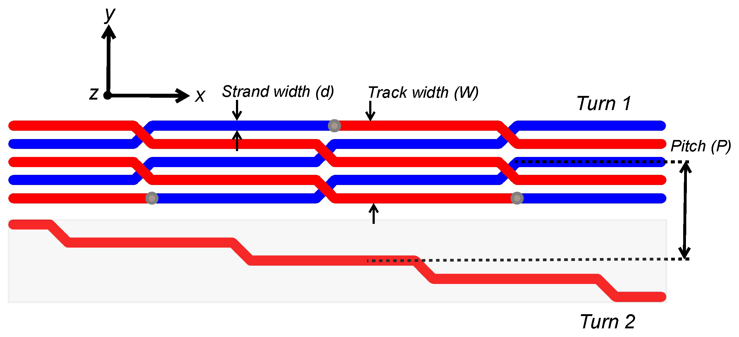
Litz style PCB with interleaving strands was first applied to planar structures and they are expected to have better AC resistance in comparison to solid PCB winding. Firstly, a one-layer solid conductor is cut into N strands. After that, the strands’ positions are gradually changed from the bottom to top layer and from the topmost to the bottommost side thanks to the use of two-layer PCB and vias as in Figure 4. By doing that, Litz style PCB has haft number of strands compared to two-layer multi-strands PCB with the same footprint and each strand is subjected to the same magnetic field, resulting in uniform current density among all strands. Moreover, because the distance between strands is large in comparison with strand width, Litz style PCB is supposed to have a significant reduction of both internal and external proximity resistances. The per unit length AC resistance of winding is just skin resistance and is expressed as in Equation (6):
R A C = R s k i n = F s k i n _ L i t z · 1 σ N d h
where N is also defined as the number of strands of Litz winding (N = 5 with the design in Figure 4), d and W are the strand width and track width, respectively.

2.4. Performance Comparison

To have an effective comparison, the windings are designed with the same footprint and dimension. Firstly, the solid winding is designed with maximum allowable track width, W = W max . After that, the multi-strands two-layer winding with the same footprint is done by stretching 2 N small parallel strands to fit the track width W m a x , each strand has width d and total copper width in each layer is W C u M u l t i S t r a n d s = N d < W m a x . Finally, the Litz style winding is created by interleaving N strands on two layers. A total of four different designs are considered as in Table 1. Some assumptions need to be included in the calculation:
-
The track pitch (P) is many times larger than PCB thickness (h) and the redistribution of current density in each track at high frequency does not affect on its external fields.
-
The Litz style winding is considered to completely remove proximity resistance.
-
The skin ratio ( F s k i n ) is considered to have a slight change while changing the track width [14].
DC resistances, AC resistances, including skin, and proximity resistances are taking into account for comparison. The per unit length resistances of each turn of a winding is summarized as in Table 2.
Table 2 shows the variation of AC resistances when applying various improvement methods. The change in conductor width does not have much improvement on skin ratios, i.e., at frequency 700 kHz, skin ratio has changed from 1.5 to 1.3 when reducing track width of 2 oz copper track from 5 mm to 2 mm, respectively [14]. Therefore, the skin resistance is considered to proportion to the copper area and R s k i n P C B 1 < R s k i n P C B 2 R s k i n P C B 3 < R s k i n P C B 4 . Proximity resistance of PCB 1 is the highest in the group because it has the larger copper width. PCB 2 has an improvement in proximity resistance in comparison to PCB 3 because it has a smaller R p r o x i m i t y _ z than PCB 3. The initial analysis shows that cutting a solid winding into strands is not better than reducing track width. Finally, in the idea Litz style PCB, the proximity effects are completely removed and it has very good AC to DC ratio, but in return, removing too much copper has significantly increased skin resistance, that can make total resistance worse than solid and multi-strands windings with same track width and number of layers.

3. Simulation and Measurement Results

In power converter with rated power to a few KVA, the switching frequency range from several kHz to 1 MHz and PCB windings with 1 oz and 2 oz copper weight are mostly used. In total, 12 windings are designed to verify the analysis results with one, three and seven turns and divided into three groups with the same number of turns and footprints. Firstly, the maximum track width of all groups is set at W m a x = 5 mm and track pitch is kept constant at P = 6 mm . After that, various improvement methods are applied to these windings to reduce AC resistance. It includes reducing track width, cutting into multiple strands and using Litz structure. The number of strands and strand width are chosen N t o t a l = 10 , d = 0.6 mm for multi-strands and N t o t a l = 5 , d = 0.6 mm for Litz windings based on the design in Reference [24], which was known to have a very good improvement on AC to DC ratio. The parameters in detail are shown in Table 3 and sample designs are presented in Figure 5.
Simulations are done by Ansys Maxwell with 3-D models and AC resistances are simulated at the following frequencies: 5 kHz (equivalent to DC), 200 kHz, 300 kHz, 500 kHz and 700 kHz. PCB parameters are chosen with copper thickness of 0.07 mm and insulator thickness of 1.62 mm, copper conductivity is set σ = 52.5 × 10 6 S / m and insulator relative permeability 1.65. AC resistances which have been extracted from PCBs 1–8 simulations indicate the total AC resistances of windings with different designs. Because simulated AC resistances cannot be separated by skin and proximity resistance, a number of simulations and measurements need to be done with one turn one layer winding as in PCBs 9–12. AC resistances of these windings are known as skin resistance and AC to DC ratios, which are ratios between AC and DC resistance of each design at a specific frequency, are used to calculated skin resistance of windings with many turns. Following that, proximity resistances are calculated by the difference between total AC resistance and skin resistance as in Equation (7). Where F s k i n is the ratio of AC to DC resistance of one turn one layer winding, R A C is the total AC resistance of a winding at a given frequency.
R s k i n = F s k i n · R D C
R p r o x i m i t y = R A C R s k i n
All windings are then produced with the same dimensions and specifications with simulated PCBs. Vector Analyzer Agilent E5061B is employed and ports 1–2 shunt method is used for resistance measurements. The designed fixture with two SMA–SMA connectors is made up as in Figure 6 and connected to PCB under test by six parallel Litz wires. By doing that, the AC resistance of the fixture is kept low in the frequency range to 700 kHz so it does not affect the measurement results. DC resistances of all windings are presented in Table 4. Simulation and experimental AC resistances of three case studies are plotted in the same graph to assess suitability as well as to verify the approximation analysis used.

3.1. Case Study 1: 1-Turn 1-Layer PCB Windings

In the first study, the PCB windings are designed with the same dimension but different styles as in Figure 7. By removing the second layer and reducing the number of turns to only one, it allows to observe the skin effect only. In the case of Litz style PCB, it is necessary to use two layers to interleave strands together, so it is impossible to design one layer PCB like one did for solid or multi-strands winding. However, because the Litz PCB is known removing a large part of its proximity resistance, in 1 turn design, it can be considered to be affected by skin resistance only. Hence, PCBs 10, 11, 12 have the same cross-sectional area and same initial DC resistance while PCB 9 has lowest DC resistance because of its largest copper width. Simulated and measured AC resistances are shown in Figure 8 (Left) and skin ratios are calculated in Figure 8 (Right).
Because Litz winding has two copper layers but solid and multi-strands winding have one layer only. Therefore, to ensure a fair comparison, skin resistance of Litz PCB (PCB 12) is compared to the equivalent skin resistance of a two-layer winding with the same footprint which is a half value of AC resistance of PCBs 9, 10 and 11 and shown in Figure 9. The results show that despite the improvement in the skin ratio, the need to remove too much copper area made the skin resistance of Litz style winding much higher than the other windings. At 500 kHz, F s k i n of Litz style PCB is equal to 76% of solid 5 mm. However, the cross-sectional area is just 30% in comparison with solid 5 mm two layers. A similar result is also obtained when comparing Litz PCB with multi-strands and solid 3 mm. For solid and multi-strands winding with the same cross-sectional area, as in PCB 10 and 11, the improvement in skin ratio and skin resistance is negligible, the difference is about 5–8% at 500 kHz and 700 kHz. These simulations and measurements are in accordance with theoretical analysis in the previous section. Furthermore, F s k i n values will be used to separate skin and proximity resistances in studies 2 and 3.

3.2. Case Study 2: 3-Turn 2-Layer PCB Windings

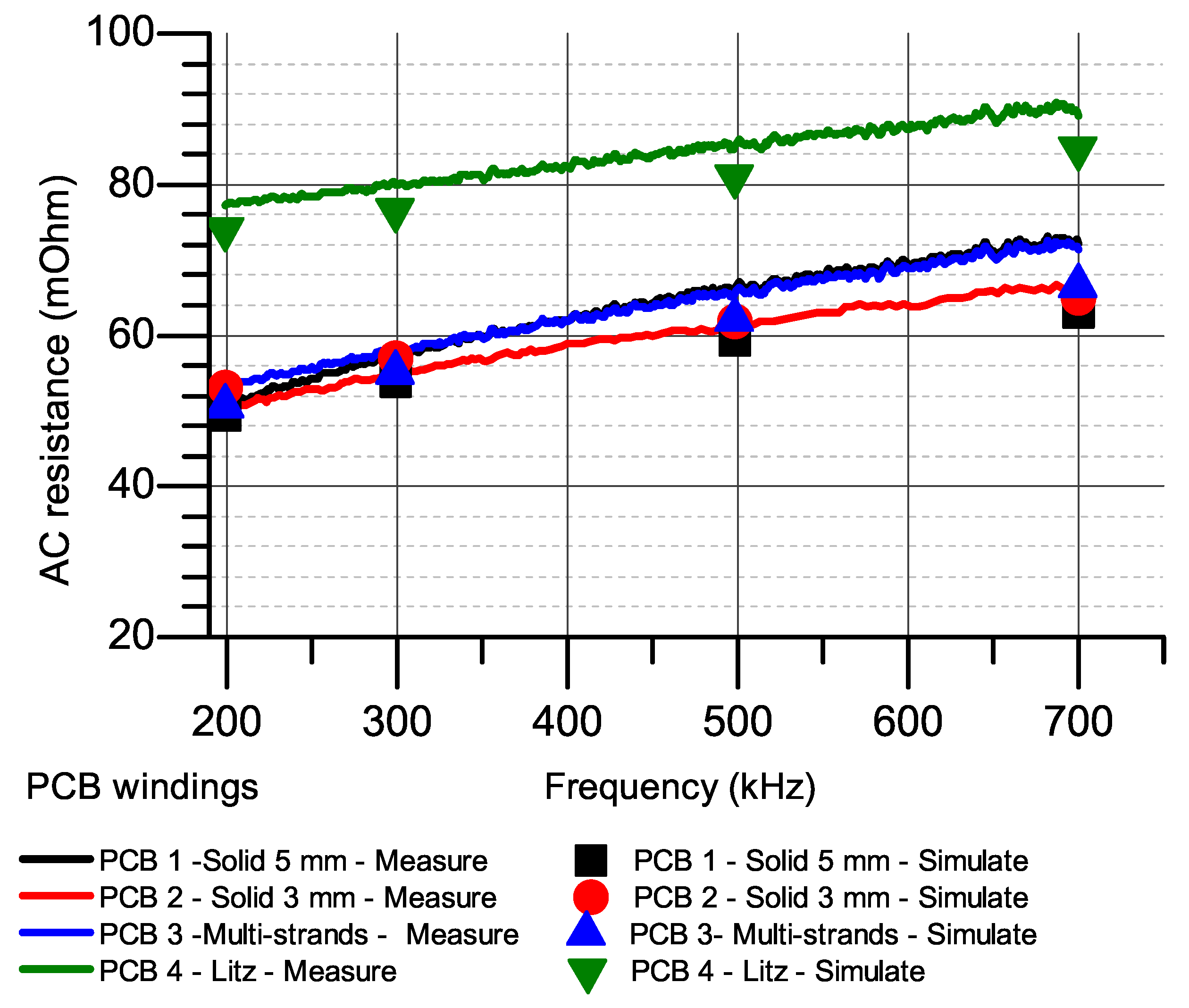
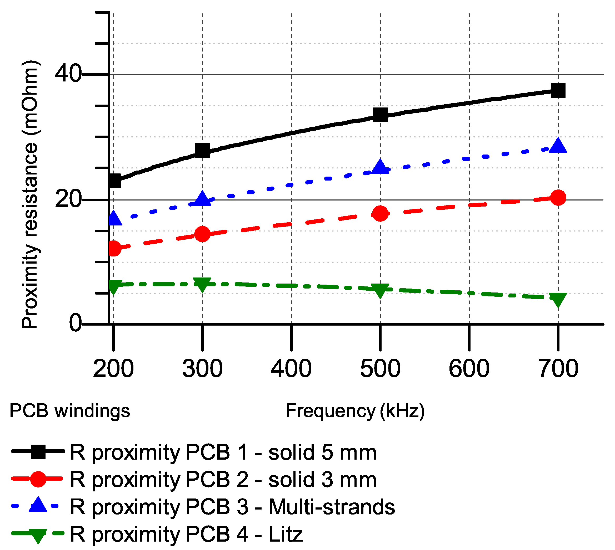
In this study, all two-layer windings have three turns with dimensions as in PCBs 1, 2 and 3 in Table 3 and Figure 10. Skin and proximity resistances are calculated based on skin ratio in Case Study 1 and Equation (7). AC resistances, including simulated and measured resistances in Figure 11 show the appropriateness of simulation and experimental results. The results show that in a winding with few turns, it is not necessary to apply improving method since solid winding already has good AC resistance. This can be explained by considering the contribution of skin and proximity resistance on the total AC resistance of a winding in Figure 12, Figure 13 and Figure 14. At 500 kHz, these values are R s k i n _ 5 m m = 32.5 m Ω and R p r o x i m i t y _ 5 m m = 34 m Ω , the contribution of proximity resistance is equal to skin resistance. Therefore, reducing the proximity resistance by reducing track width or using multi-strands winding has no significant improvement, since it has increased the skin resistance. In comparison between multi-strands and solid PCB with the same cross-sectional area, the proximity resistance of multi-strands winding (PCB3) is larger than solid (PCB2) at 500 kHz and 700 kHz. This measurement result is consistent with the previous conclusion that there is no improvement with proximity resistance when cutting solid winding into small strands in parallel. Finally, the Litz style winding has the best AC to DC ratio with proximity resistance almost eliminated. However, because of the smallest cross-sectional area, it has the largest AC resistance among the windings.

3.3. Case Study 3: 7-Turn 2-Layer PCB Windings

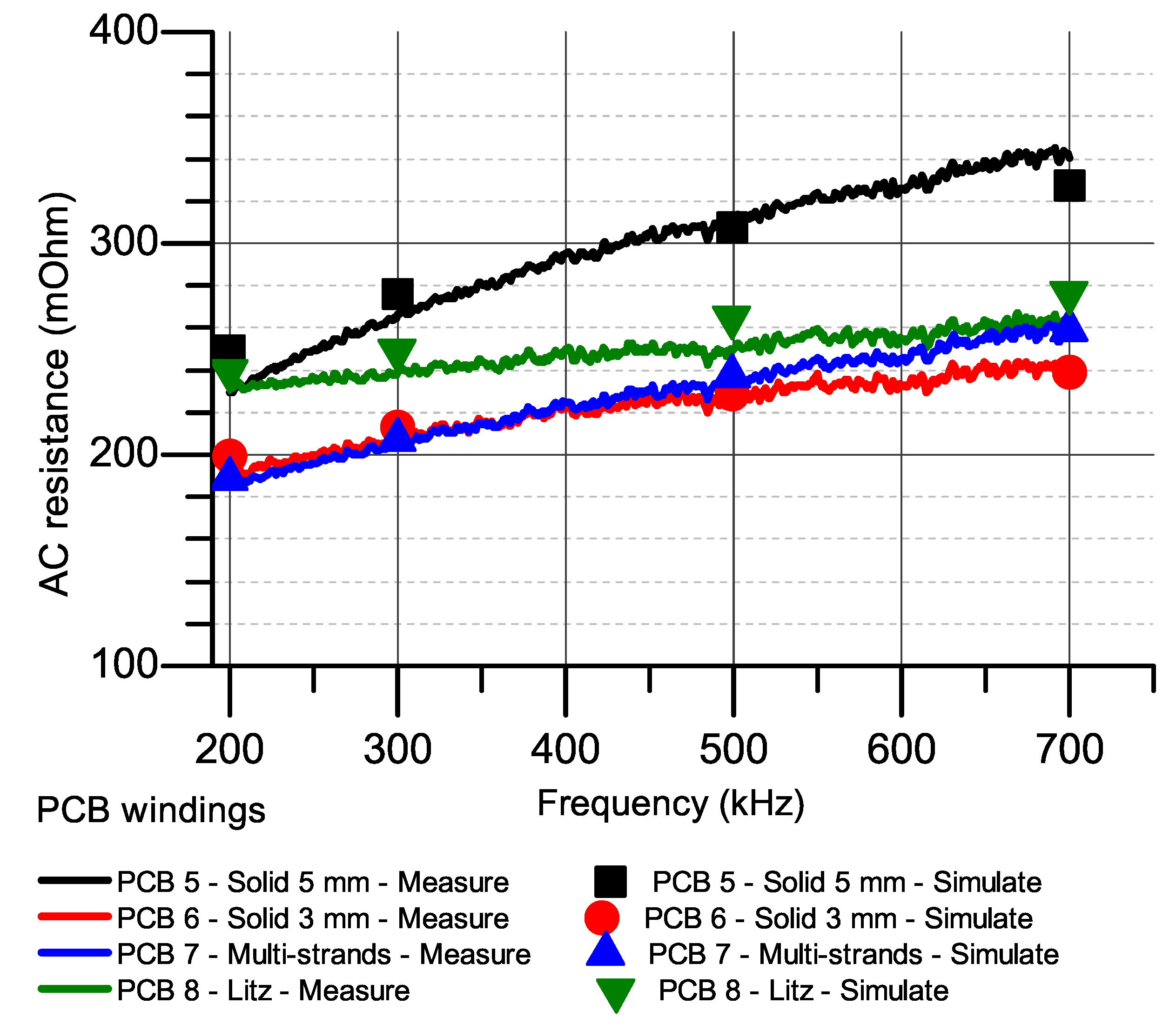
In the last study, windings are designed with seven turns as in PCB 5, 6, 7, 8 on Table 3 and Figure 15. The measurement and simulation steps are also repeated as in Case Study 2 and results are shown in Figure 16, Figure 17, Figure 18 and Figure 19. PCB 5 with track width 5 mm has the highest AC resistance because it is mostly influenced by proximity effect. At 500 kHz, these values are R s k i n _ P C B 5 = 95 m Ω and R p r o x i m i t y _ P C B 5 = 215 m Ω , which proximity resistance is about 2.26 times compared to skin resistance. Therefore, optimal methods need to be applied to reduce this value. Optimal methods show a significant improvement in AC resistance at high frequency because they have eliminated a majority of proximity resistance. These values are R p r o x i m i t y _ P C B 6 = 85 m Ω , R p r o x i m i t y _ P C B 7 = 103 m Ω and R p r o x i m i t y _ P C B 8 = 10 m Ω at 500 kHz, which is many times smaller than proximity resistance of PCB 5. PCB 5 and 6 have the same AC resistance in the frequency range to 500 kHz and then the AC resistance of PCB 5 is smaller than PCB 6 at 700 kHz. This is consistent with the theoretical analysis in the previous section and again shows the stranded winding does not have much help in reducing AC resistance compared to reducing track width. Litz PCB in applications with many turns windings has shown a significant improvement in AC resistance compared to maximum track width. However, because of keeping AC resistance stable at high value in a wide frequency range has made worse losses in the low frequency region.

4. Discussion

4.1. AC Resistances at Higher Frequency

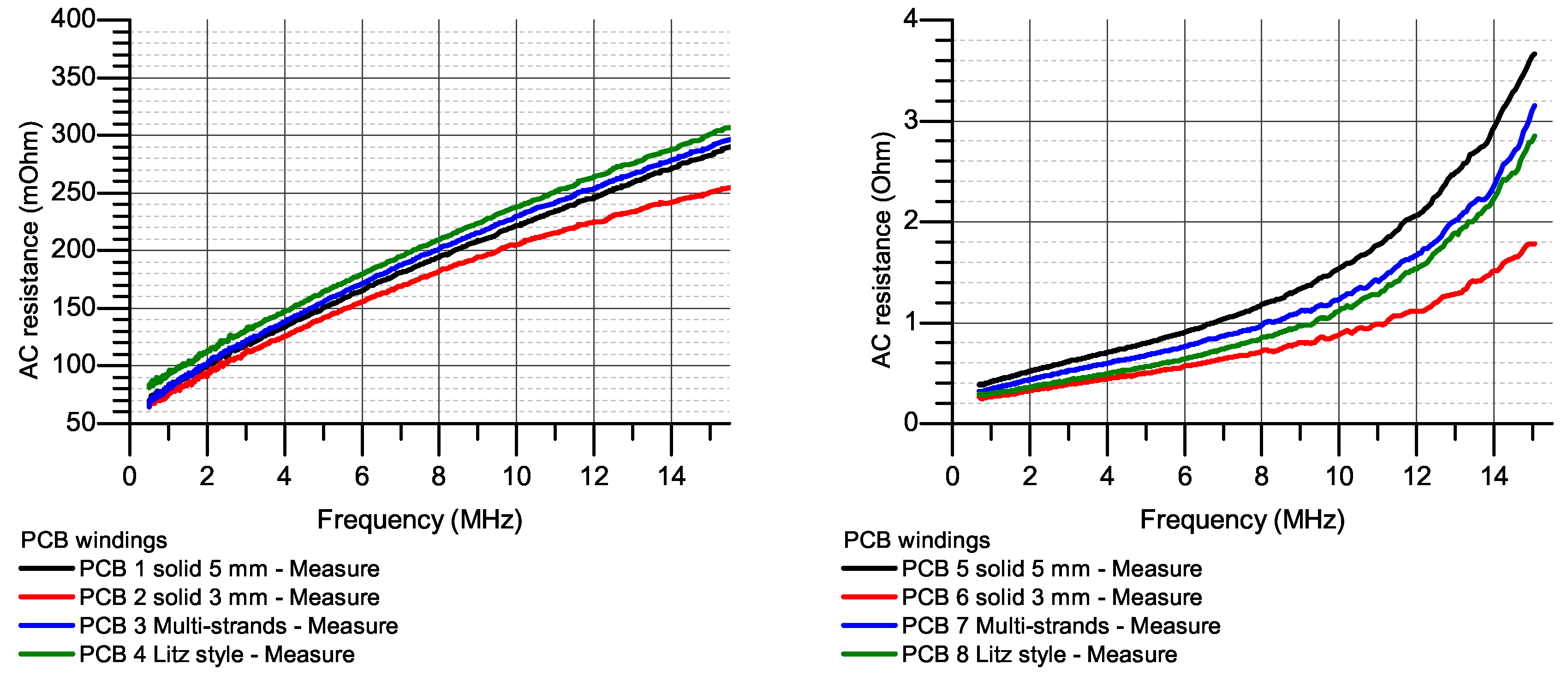
To better understand the behaviour of different PCB windings, measurements are done in a range from 1 MHz to 15 MHz, which is known as frequency range of higher order harmonics of power converters. Because impedance of 3-turn and 7-turn PCB windings become larger in this range, the port 2 reflection method is used to measure and extract AC resistances and impedance of PCBs 1–8 windings. Measurement results in Figure 20 show that improving AC resistance by reducing track width still gives a good result over a wide range of frequency.

4.2. Pros and Cons of Each Winding Style

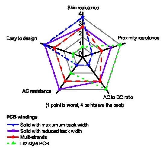
Simulation and measurement results, along with mathematical analysis, have shown the pros and cons of each improvement. The AC to DC ratios between the two winding groups with different number of turns in Figure 21 show that Litz PCB has a stable total AC resistance to DC resistance ratio ( F r ) when both the frequency and number of turns of windings have changed. However, the need to eliminate a large copper area has made Litz winding worse resistance than adaptive solid winding. Figure 21 also shows that the Fr value should not be used to evaluate the improvement of AC resistance and the performance of an optimal method. Therefore, five comparison points, including skin resistance, proximity resistance, AC to DC ratio, total AC resistance and complexity should be taken into consideration when choosing a PCB winding design, as presented in Figure 22. At low frequency, the winding resistance is determined by skin resistance, which is directly related and tends to decrease as the conductance cross-sectional area increases. At high frequency, or when the proximity effect becomes serious, optimal methods should be applied to reduce winding losses. The use of multi-strand winding is not recommended due to its complex design and unclear performance while the use of solid PCB with optimal track width shows a clearer improvement in AC resistance. Litz style PCB, which is well known for its AC on DC ratios and very good proximity resistance should be used for winding that have many turns or in equipment that needs stability of resistance in a wide frequency range.

5. Conclusions

This paper has presented a general review of improving methods applied to the reduction of AC resistance of a PCB winding and shows the advantages and disadvantages of each improvement. It also points out the need to use absolute AC resistance as a main comparing factor in designs PCB winding, instead of AC to DC ratio. In addition, this paper also shows the contribution of skin and proximity resistance in a winding and with a conclusion that: at high frequency, the AC resistance of a winding is greatly affected by proximity resistance while at low frequency, skin resistance is decisive for the AC resistance of a winding. Thus, an appropriate method should be used for each application.

Author Contributions

M.H.N. did the analysis, simulations and verified the results with measurement prototypes. H.F.B. provided supervision and manuscript revised. All authors have read and agreed to the published version of the manuscript.

Funding

This research has been funded by the NSERC under grant number RGPIN 2019-07128.

Conflicts of Interest

The authors declare no conflict of interest.

Abbreviations

The following abbreviations are used in this manuscript:
σ Copper conductivity
δ Copper skin depth
ω Angular frequency
B x Average external magnetic field parallel to X Axis
B z Average external magnetic field parallel to Z Axis
dStrand width
FEMFinite element simulation
F s k i n Ratio of AC resistance causes by skin effect to DC resistance
F p r o x i m i t y Ratio of AC resistance causes by proximity effect to DC resistance
F r Ratio of total AC resistance to DC resistance
hTrack thickness
IExcitation current or main current
L o u t Outer length of a winding
MMFMagnetomotive Force
NNumber of strands of one layer of multi-strand winding or Number of strands of Litz style winding
N t o t a l Total number of strands of a winding
PTrack pitch
R A C Total AC resistance causes by skin and proximity effects
R D C DC resistance
R s k i n AC resistance causes by skin effect
R p r o x i m i t y AC resistance causes by proximity effect
STrack distance
tPCB thickness or layer distance
VNAVector Network Analyzer
WTrack width
W o u t Outer width of a winding

References

  1. Li, B.; Li, Q.; Lee, F.C. High-Frequency PCB Winding Transformer With Integrated Inductors for a Bi-Directional Resonant Converter. IEEE Trans. Ind. Electron. 2019, 34, 6123–6135. [Google Scholar] [CrossRef]
  2. Ouyang, Z.; Thomsen, O.C.; Andersen, M.A.E. Optimal Design and Tradeoff Analysis of Planar Transformer in High-Power DC–DC Converters. IEEE Trans. Ind. Electron. 2012, 59, 2800–2810. [Google Scholar] [CrossRef]
  3. Marian, K. Kazimierczuk, Proximity Effect. In High Frequency Magnetic Components, 2nd ed.; Wiley: Coshocton, OH, USA, 2014; p. 226. [Google Scholar]
  4. Barrios, E.L.; Urtasun, A.; Ursúa, A.; Marroyo, L.; Sanchis, P. High-Frequency Power Transformers with Foil Windings: Maximum Interleaving and Optimal Design. IEEE Trans. Ind. Electron. 2015, 30, 5712–5723. [Google Scholar] [CrossRef]
  5. Zhao, B.; Ouyang, Z.; Anderson, M.A.E.; Duffy, M.; Hurley, W.G. An improved partially interleaved transformer structure for high-voltage high-frequency multiple-output applications. In Proceedings of the IECON 2017-43rd Annual Conference of the IEEE Industrial Electronics Society, Beijing, China, 29 October–1 November 2017; pp. 798–804. [Google Scholar]
  6. Youssouf, K.; Kahlouche, F.; Soultan, M.; Youssouf, M.; Bechir, M.H.; Capraro, S.; Chatelon, J.P.; Siblini, A.; Siblini, J.J. Design and Study of Interleaved and Face to Face Magnetic Microtransformers. IEEE Trans. Electron. Devices 2014, 61, 2873–2878. [Google Scholar] [CrossRef]
  7. Thummala, P.; Schneider, H.; Zhang, Z.; Andersen, M.A.E. Investigation of Transformer Winding Architectures for High-Voltage (2.5 kV) Capacitor Charging and Discharging Applications. IEEE Trans. Ind. Electron. 2016, 31, 5786–5796. [Google Scholar] [CrossRef]
  8. Lee, C.K.; Su, Y.P.; Hui, S.Y.R. Printed Spiral Winding Inductor With Wide Frequency Bandwidth. IEEE Trans. Ind. Electron. 2011, 26, 2936–2945. [Google Scholar] [CrossRef] [Green Version]
  9. Saket, M.A.; Shafiei, N.; Ordonez, M. Planar transformer winding technique for reduced capacitance in LLC power converters. In Proceedings of the 2016 IEEE Energy Conversion Congress and Exposition (ECCE), Milwaukee, WI, USA, 18–22 September 2016; pp. 1–6. [Google Scholar] [CrossRef]
  10. Stadler, A.; Albach, M.; Macary, F. The minimization of copper losses in core-less inductors: Application to foil- and PCB-based planar windings. In Proceedings of the 2005 European Conference on Power Electronics and Applications, Dresden, Germany, 11–14 September 2005. [Google Scholar] [CrossRef]
  11. Marian, K. Kazimierczuk, Winding resistance at high frequencies. In High Frequency Magnetic Components, 2nd ed.; Wiley: Coshocton, OH, USA, 2014; p. 303. [Google Scholar]
  12. Su, Y.; Liu, X.; Lee, C.K.; Hui, S.Y. On the relationship of quality factor and hollow winding structure of coreless printed spiral winding (CPSW) inductor. IEEE Trans. Ind. Electron. 2012, 27, 3050–3056. [Google Scholar]
  13. Kim, D.-H.; Park, Y.-J. Calculation of the inductance and AC resistance of planar rectangular coils. Electron. Lett. 2016, 52, 1321–1323. [Google Scholar] [CrossRef]
  14. Nguyen, M.H.; Fortin Blanchette, H. Optimizing AC Resistance of Solid PCB Winding. Electronics 2020, 9, 875. [Google Scholar] [CrossRef]
  15. Varghese, B.J.; Smith, T.; Azad, A.; Pantic, Z. Design and optimization of decoupled concentric and coplanar coils for WPT systems. In Proceedings of the 2017 IEEE Wireless Power Transfer Conference (WPTC), Taipei, Taiwan, 10–12 May 2017; pp. 1–4. [Google Scholar]
  16. Lope, I.; Carretero, C.; Acero, J.; Burdío, J.M.; Alonso, R. PCB multi-track coils for domestic induction heating applications. In Proceedings of the IECON 2012-38th Annual Conference on IEEE Industrial Electronics Society, Montreal, QC, Canada, 25–28 October 2012; pp. 3287–3292. [Google Scholar]
  17. Serrano, J.; Lope, I.; Acero, J.; Carretero, C.; Burdío, J.M. Mathematical description of PCB-adapted litz wire geometry for automated layout generation of WPT coils. In Proceedings of the IECON 2017-43rd Annual Conference of the IEEE Industrial Electronics Society, Beijing, China, 29 October–1 November 2017; pp. 6955–6960. [Google Scholar]
  18. Lope, I.; Carretero, C.; Acero, J.; Alonso, R.; Burdío, J.M. AC Power Losses Model for Planar Windings with Rectangular Cross-Sectional Conductors. IEEE Trans. Ind. Electron. 2014, 29, 23–28. [Google Scholar] [CrossRef]
  19. Wang, S.; de Rooij, M.A.; Odendaal, W.G.; van Wyk, J.D.; Boroyevich, D. Reduction of high-frequency conduction losses using a planar litz structure. IEEE Trans. Ind. Electron. 2005, 20, 261–267. [Google Scholar] [CrossRef]
  20. Lope, I.; Acero, J.; Serrano, J.; Carretero, C.; Alonso, R.; Burdio, J.M. Minimization of vias in PCB implementations of planar coils with litz-wire structure. In Proceedings of the 2015 IEEE Applied Power Electronics Conference and Exposition (APEC), Charlotte, NC, USA, 15–19 March 2015; pp. 2512–2517. [Google Scholar]
  21. Rehlaender, P.; Grote, T.; Tikhonov, S.; Niejende, H.; Schafmeister, F.; Bocker, J.; Thiemann, P. A PCB Integrated Winding Using a Litz Structure for a Wireless Charging Coil. In Proceedings of the 2019 21st European Conference on Power Electronics and Applications (EPE’19 ECCE Europe), Genova, Italy, 2–5 September 2019; pp. pp. P.1–P.9.
  22. Kuhn, W.B.; Ibrahim, N.M. Analysis of current crowding effects in multiturn spiral inductors. IEEE Trans. Microw. Theory Tech. 2001, 49, 31–38. [Google Scholar] [CrossRef] [Green Version]
  23. Hurley, W.G.; Gath, E.; Breslin, J.G. Optimizing the AC resistance of multilayer transformer windings with arbitrary current waveforms. IEEE Trans. Ind. Electron. 2000, 15, 369–376. [Google Scholar] [CrossRef] [Green Version]
  24. Lope, I.; Carretero, C.; Acero, J.; Alonso, R.; Burdio, J.M. Frequency-Dependent Resistance of Planar Coils in Printed Circuit Board With Litz Structure. IEEE Trans. Magn. 2014, 50, 8402409. [Google Scholar] [CrossRef]
Figure 1. Non-interleaving windings (Left) and interleaving windings (Right).
Electronics 09 01324 g001
Figure 2. A copper track under external field.
Electronics 09 01324 g002
Figure 3. Equivalent model of multi-strands conductor.
Electronics 09 01324 g003
Figure 4. Two-layer Litz style PCB tracks with top layer in red, bottom layer in blue (Upper track) and an extracted interleaving strand (Lower track).
Electronics 09 01324 g004
Figure 5. Litz PCB 3 turn winding (Left), multi-strands winding (Middle) and solid PCB winding (Right).
Electronics 09 01324 g005
Figure 6. Measurement setup.
Electronics 09 01324 g006
Figure 7. Single turn PCB windings with solid 5 mm (Top Left), solid 3 mm (Top Right), multi-strands (Bottom Left) and Litz style (Bottom Right).
Electronics 09 01324 g007
Figure 8. Simulated and measured skin resistances (Left) and skin ratio (Right) of different windings.
Electronics 09 01324 g008
Figure 9. Calculated equivalent skin resistances of one turn two layers windings.
Electronics 09 01324 g009
Figure 10. Three turn PCB windings with solid 5 mm (Top left), solid 3 mm (Top right), multi-strands (bottom left) and Litz style (bottom right).
Electronics 09 01324 g010
Figure 11. Measured and simulated AC resistances of 3-turn windings.
Electronics 09 01324 g011
Figure 12. Calculated skin and proximity resistances of 3-turn windings.
Electronics 09 01324 g012
Figure 13. Calculated skin resistances of 3-turn windings.
Electronics 09 01324 g013
Figure 14. Calculated proximity resistances of 3-turn windings.
Electronics 09 01324 g014
Figure 15. Seven-turn PCB windings with solid 5 mm (Top left), solid 3 mm (Top right), multi-strands (bottom left) and Litz style (bottom right).
Electronics 09 01324 g015
Figure 16. Measured and simulated AC resistances of 7-turn windings.
Electronics 09 01324 g016
Figure 17. Calculated skin and proximity resistances 7-turn windings.
Electronics 09 01324 g017
Figure 18. Calculated skin resistances of 7-turn windings.
Electronics 09 01324 g018
Figure 19. Calculated proximity resistances of 7-turn windings.
Electronics 09 01324 g019
Figure 20. AC resistances of 3-turn windings (Left) and 7-turn windings (Right) at higher frequency range.
Electronics 09 01324 g020
Figure 21. Calculated AC to DC ratio of 3-turn windings (Left) and 7-turn windings (Right).
Electronics 09 01324 g021
Figure 22. Comparison among PCB winding design methods with high impact of proximity effect.
Electronics 09 01324 g022
Table 1. Two layers PCB profiles and parameters.
NoProfile NamesTrack WidthTrack PitchStrand WidthTotal Number of Strands N total
PCB1Solid with maximum track width W max P--
PCB2Solid with reduced track width N d P--
PCB3Multi-strands W max Pd2N
PCB4Litz style PCB W max PdN
Table 2. Per unit length resistances of each turn of different windings.
NoProfile NamesDC ResistanceSkin ResistanceProximity Resistance
PCB1Solid with maximum track width 1 2 σ W max h F s k i n _ s o l i d 2 σ W max h 1 24 h ω 2 σ B z 2 W max 3 + 1 24 W max ω 2 σ B x 2 h 3
PCB2Solid with reduced track width 1 2 σ N d h F s k i n _ s o l i d 2 σ N d h 1 24 h ω 2 σ B z 2 N d 3 + 1 24 N d ω 2 σ B x 2 h 3
PCB3Multi-strands 1 2 σ N d h F s k i n _ m u l t i s t r a n d s 2 σ N d h 1 24 h ω 2 σ B z 2 N d W max 2 + 1 24 N d ω 2 σ B x 2 h 3
PCB4Litz style PCB 1 σ N d h F s k i n _ L i t z σ N d h 0
Table 3. Two ounces two-layer winding parameters.
GroupNoDescriptionsNumber of TurnsOuter Length
L out ( mm )
Outer Width
W out ( mm )
Track Width
W ( mm )
Strand Width
d ( mm )
Total Number
of Strands N total
Group 1PCB 1Solid winding 2 layers3112435--
PCB 2Solid winding 2 layers3112433--
PCB 3Multi-strands winding 2 layers31124350.610
PCB 4Litz winding 2 layers31124350.65
Group 2PCB 5Solid winding 2 layers7160915--
PCB 6Solid winding 2 layers7160913--
PCB 7Multi-strands winding 2 layers71609150.610
PCB 8Litz winding 2 layers71609150.65
Group 3PCB 9Solid winding 1 layer1160915--
PCB 10Solid winding 1 layer1160913--
PCB 11Multi-strands winding 1 layer11609150.65
PCB 12Litz winding 2 layers11609150.65
Table 4. DC resistances of PCB prototypes.
GroupPCBsDescriptions R DC measure
m Ω
R DC simulate
m Ω
R DC measure R DC simulate
m Ω
Group 1 (Three-Turn PCBs)PCB 1solid 5 mm22.521.280.7
PCB 2solid 3 mm33.134.781.68
PCB 3multi-strands38.235.272.93
PCB 4Litz PCB7470.573.43
Group 2 (Seven-Turn PCBs)PCB 5solid 5 mm65.369.834.53
PCB 6solid 3 mm107.11146.9
PCB 7multi-strands107.96114.56.54
PCB 8Litz PCB222226.644.64
Group 3 (One-Turn PCBs)PCB 9solid 5 mm24.5726.51.93
PCB 10solid 3 mm43.244.10.9
PCB 11multi-strands39.7643.543.78
PCB 12Litz PCB38.6144.896.28