Review

Review of Solid State Transfer Switch on Requirements, Standards, Topologies, Control, and Switching Mechanisms: Issues and Challenges

by
Mohammad Faisal
1,
Mahammad Abdul Hannan
1,*,
Pin Jern Ker
1,
Muhamad Safwan Bin Abd Rahman
1,
Mohammad Sazib Mollik
2 and
Muhamad Bin Mansur
1
1
Department of Electrical Power Engineering, Universiti Tenaga Nasional, Kajang 43000, Selangor, Malaysia
2
UNITEN R & D Sdn Bhd, Universiti Tenaga Nasional, Kajang 43000, Selangor, Malaysia
*
Author to whom correspondence should be addressed.
Electronics 2020, 9(9), 1396; https://doi.org/10.3390/electronics9091396
Submission received: 23 June 2020 / Revised: 30 July 2020 / Accepted: 31 July 2020 / Published: 28 August 2020
(This article belongs to the Section Systems & Control Engineering)

Abstract

:
Large-scale industrial loads, sensitive loads, and electrical power distribution systems suffer from power quality issues such as voltage interruptions, flickering, and sags which can cause a significant financial loss. The semiconductor based solid-state transfer switch (SSTS) can utilize the dual power feeders to protect the loads against these power disturbance issues. Conventional SSTS often requires more than quarter cycles to complete the transfer process because of load dependent commutation. Numerous researchers proposed the improved SSTS with impulse commutated circuit, which can reduce the transfer time and provide better ride-through capability against voltage sags. However, the SSTS specification depends on the application types and design procedure. Recently, hybrid SSTS has been introduced by the researchers to overcome all these issues. It has been investigated that not much papers are available in literature so far to aggregate all these issues. Therefore, towards the novel contribution of research, this review critically described the requirements, standards, and specifications of SSTS; control and switching mechanisms; and application of SSTS as single or hybrid topology, to give a comprehensive idea to the future researchers about the design of SSTS for a specific application. This paper also contributes to analyzing the key issues related to the SSTS applications, which can provide an easy control strategy and reduce the transfer time significantly. Overall, this research will strengthen the efforts of the researchers and industrialists to select, develop, and design the appropriate SSTS for a particular application.

1. Introduction

Transfer time of traditional mechanical switches to switch the fault power to the alternate power during interruption approximately ranges between 6 to 36 cycles. These switches are applied in most of the medium and high voltage applications previously. Mechanical switches are not ideal because of the inherent characteristics, switching speed, and longer switch action [1]. In contrast, during switching of automatic transfer switch (ATS), arcing phenomena or vibration takes place which may cause erosion, heat, energy loss, and electromagnetic disturbance towards reducing the life expectancy of the switch. If the heat does not release in time, they may damage the semiconductor devices. Hence, they need to be equipped with a large capacity cooling system [2]. However, ATS is advantageous in improving the power quality and reliability through voltage sag and power interruption minimization. There are four basic types of automatic transfer switches: break-before-make (open transition), make-before-break (closed), delayed transition (center off), and solid-state switch. Solid-state switches are often used in switch matrix systems for testing of semiconductor devices, where high switching speed is critical and power handling requirements are lower. Applications of solid-state transfer switch to power the susceptible loads effectively reduces the loss induced by the switching devices [3].
Recent industrial facilities consist of various sensitive loads which require high-quality power for stable operation and reduce the rapid voltage interruption problems such as voltage sag, voltage swell, flickering, etc. According to the American Electric Power Research Institute (EPRI), 98% of total transient power quality problem occurs due to voltage sags which may cause huge economic losses [4] in the large industrial sectors. Impact of manual versus automatic transfer switching in industrial plants has been demonstrated in [5]. Using zone branch methodology for the reliability evaluation, it is observed that the annual load point interruption during manual switching is 1.2–3.1 times higher than when automatic transfer procedures of restoration were used. An automatic transfer scheme is established in Tenaga Nasional Berhard Distribution Negeri Perak to perform the automatic switching safely to minimise interruption down approximately 1 s or faster [6]. The proposed scheme can optimize the utilization of manpower and operational cost, which can be implemented in the existing control system. With the rapid development of technologies on wide bandgap semiconductor devices, such as silicon carbide (SiC), static induction transistors (SITs), SiC metal oxide semiconductor field effect transistors (MOSFETs), and SiC junction gate field effect transistors (JFETs) can provide superior switching performance and are much better than the mechanical counterparts to solver the power quality issues [7]. Researchers identify solid-state transfer switches (SSTS) as a possible cost-effective solution to power quality problems [8,9] in all kinds of small, medium, and large scale industries. Solid-state circuit breakers (SSCB) which is also commonly known as SSTS, can be used to solve the aforementioned disturbances regarding the power quality issues. This type of custom power devices replaced the traditional solution techniques of using ferro-transformer, reactors, to solve the voltage flickering, voltage sags, etc. Study indicates that silicon-controlled rectifier (SCR)-based bypass switches have a worse dynamic in turn-off characteristic, so that the critical load may suffer from severe grid faults for a long time. An SCR-based transfer switch is presented in a double-fed machine (DFM) drive where two sets of SCRs are proposed for low speed (dc mode) and high speed (ac mode). This technique minimizes switching losses without increasing harmonic distortions of stator waveform [10].
A schematic of an ideal transfer switch for DFM that presented in [10] is depicted in Figure 1. From the figure, the DFM can be connected with either ac or dc sources, depending on the configuration of switch S1 or S2. A rectifier is used to convert the ac source into a dc source. The dc source supplies resistive losses in the stator of DFM. Consequently, the power rating of the transformer rectifier is a fraction of the DFM power rating.
The IEEE benchmark system of static transfer switch (STS) STS-1 (IEEE PES TF 2001) is shown in Figure 2 in which it consists of two sets of three-phase solid-state static switches, one for the main feeder and the other one for the back-up feeder. Each switch is arranged with anti-parallel thyristors having fast transfer characteristics from the main feeder (after disturbance) to back-up feeder [11]. Generally, the thyristors of the main feeders are continuously energized and while the thyristors of the back-up feeder are in a de-energized position. If a fault occurs in the main feeder, the firing pulses of the thyristors in the main feeder stopped the thyristors from conducting at first natural current zero, and the thyristors of the back-up feeder are turned ON to transfer the load from the main feeder to back-up feeder. When the fault in the main feeder is cleared, the process is reversed to transfer the load to the main feeder again.
Recently, integrated gate commutated thyristors (IGCTs) and insulated gate bipolar transistors (IGBTs) based solid-state switches have been reported in various researches [12]. Study shows that the recent technological advancement in power electronics and power semiconductor devices like thyristors, gate turn-off thyristors (GTO), triode for alternating current (TRIAC), and integrated gate bipolar transistors (IGBTs) allow the transfer time within a quarter of a cycle (equivalent to 5 ms) [13,14]. The transfer time of RL loads, regenerative loads and cross current phenomena of thyristor based transfer switch have been studied in [15], where it is stated that the transfer system has less impact to the critical loads. The transfer switch is used to protect sensitive loads from system side faults by swiftly transferring the load to an alternate one. The consequence of the system side faults may be the voltage sags, voltage swells, or power interruption. SPST and SPDT based bistable relays have been proposed as transfer switch in [16]. The disadvantage of this research is that it does not match with the older systems. Authors in [17] proposed the high-performance magnetic refrigeration using a solid-state thermal switch instead of using the hydraulic component. When a magnetic field is applied to the system, the thermal conductivity of one thermal switch (connected to the hot reservoir) increases compare to alternate one (connected to the cold reservoir), consequently heat conduction occurs. When the magnetic field is removed, the reverse process takes place. Here, a solid-state thermal switch is used as an alternative to the fluids. Authors in [18] proposed to use thyristors in designing SSTS as thyristors have has fewer conduction losses compared to GTO. In this research, an electromagnetic transient simulation program (PSCAD/EMTDC) is used to observe the performance of SSTS in protecting the distribution system. Here, SSTS transfers the power to the load from faulty feeder to a healthy one in a short period (less than half cycle or 10 ms). Figure 3 shows the proposed SSTS fault detection and transfer mechanism.
According to the figure, equations for transforming the instantaneous three-phase voltages Va(t), Vb(t), and Vc(t) into the αβ-coordinate system and then further conversion into rotating dq-coordinate system can be expressed by
[ V α ( t ) V β ( t ) V 0 ( t ) ] = 2 3 [ 1 1 2 1 2 0 3 2 3 2 1 2 1 2 1 2 ] [ V a ( t ) V b ( t ) V c ( t ) ]   ,
V ( d q ) ( t ) = e j θ ( t ) V ( α β ) ( t ) ,
where, V0 (t) denotes the zero-sequence voltage component and θ (t) represents the transformation angle which can be obtained by
θ ( t ) = θ ( 0 ) + 0 t ω ( t ) d t ,
now, to calculate the amplitude of the supply voltage vector, Vdq(t), in dq-cordinate
V d q ( t ) = ν 2 d ( t ) + ν 2 q ( t ) ,
where, the term v2d(t) and v2q(t) represent the d-component and q-component voltage. The amplitude of the supply voltage is compared with the threshold voltage, V(dq)ref(t) in accordance with the sensitivity of the load to detect the fault signal. It is noted that the fault detection time depends on the nature of faults and the various types of voltage sag phenomena. Considering various load conditions and having a higher cut-off frequency, it is proven that the proposed SSTS successfully detects the faults faster in case of static RL load compare to the topology with induction motor load and hybrid load.
The authors in [10] extended their research for the same DFM applications where they have proposed 8 thyristors instead of 12 [19]. Mitigating the voltage unbalance and to reduce the power loss in bipolar low voltage dc distribution system is proposed in [20] where IGBT-based static load transfer switch (SLTS) algorithm is used to generate the switching signals in reconfiguring the structure of loads. Application of SSCB in 1 kV dc distribution system for shipboard applications has been described in [21] which can isolate the fault with less than 50 µs. In this research, a switchboard-based control (SBC) system is used as the back-up protection of SSCB to observe the undervoltage condition and trip the breaker. The testbed is emulated with power hardware-in loop (PHIL) software. However, overvoltage protection is avoided in this research. A logic gate based intelligent control of SSTS on supplying the power has been discussed in [22], where multiple sources and multiple switches are connected for managing the load and keep the uninterrupted power supply in the building. This topology reduces the losses during the transfer time. To avoid the weak turn-off capabilities of IGCTs, a mixer solid state switch (MSS) for a hybrid DC circuit breaker (HCB) has been proposed in [23] to reduce the cost of traditional SSTS. Both the IGCTs and IGBTs have been are integrated for this purpose. Figure 4 depicts the requirements of solid state switch in HCB and the model is developed in Silvaco TCAD. When a fault occurs, the mechanical switch is triggered to isolate the system, and the fault current is forced to commutate to the solid-state switch by the current commutation equipment (usually a load commutation switch). Then, the solid-state switch continues to conduct the current until the distance between the mechanical switch contacts is sufficient to withstand overvoltage. Although these topologies have contributed to the development of SSTS based applications, authors in [24] highlighted the asymmetrical characteristics of the high-voltage power devices as the barrier in achieving bidirectional functionality. A diode-bridge bidirectional solid-state switch has been proposed in [25] as a cost-effective solution for high voltage DC circuit breaker, where the solid-state switch is used in conjunction with the mechanical switch and current commutation equipment. Hence, the cost is an important determinant for the application of SSTS.
Two common processes, such as break-before-make (BBM) and make-before-break (MBM), are generally available for controlling SSTS. In the BBM method, when the primary current ceased then transfer from the main feeder to alternate feeder takes place whereas when MBB mechanism is used, the load transfer occurs before the current has expired. The benefit of MBB over BBM is that it has faster transfer time [8]. On the other hand, MBB suffers from the generation of high surge current, which may damage the system. Hence, overcoming this limitation of MBB mechanism is a prime concern of future researchers. Various studies have been conducted for SSTS control strategies and applications. Although research on SSTS applications in distribution system [18], impulse commutation bridge [26], uninterrupted power supply [3], double-fed machine drive [19], etc. have been demonstrated separately, no comprehensive review has been found so far to describe the SSTS design requirements, standards, available SSTS specifications, control topologies, and their various applications. Thus, the significant contribution of this paper can be summarized as follows:
(i)
This study provides a comprehensive idea about the requirements, standards, and specifications of SSTS towards the selection, development, and design of SSTS.
(ii)
This research illustrates the various SSTS control strategies and switching mechanisms including make-before-break, break-before-make, and commutation strategies.
(iii)
This work describes the various applications of SSTS, SSCB as SSTS, hybrid SSTS and addresses the issues and challenges towards the development of SSTS. The key findings will benefit researchers and industrialists for the future scope of applications.

2. Requirements, Standards and Specifications

IEC has stringent requirements for transfer switches in IEC 60947-6-1 and IEC 60947-6-3. UL 1008 requires that the fourth pole of a transfer switch be tested and proven to have ratings equal to its phase contacts if not of the same construction [27]. When switching medium voltages and high currents, circuit breakers having electronically controlled and interlocked characteristics need to consider. These schemes usually employ protective relays, fast communication protocols, and extensive check and lockout logic. An electrical control/interlocking bypass system using properly rated mechanisms can be a better choice than a single transfer switch, however, it is costly [28]. The solid state switch is advantageous compared to electromechanical or mechanical switches as it has no moving parts and eliminates the noise and transients. SSTS is employed to provide faster transfer of source (preferred source to alternate source) or load in case of system fault, which occurs in a fraction of power cycle. Besides, the SSTS needs to be designed or rated considering the steady state or transient voltage in the transmission and distribution system during load transfer or when any voltage disturbance is detected in the preferred source. For long distance transmission systems where the higher voltage is required, the AC system is usually preferred as it is easier to generate higher frequency AC voltage by using a transformer and can be controlled or protected by a transfer switch mechanism. This system provides the safe transmission with reduced losses. On the other hand, in the case of a DC grid system, the conversion is easier and hence the conduction loss and material costs are reduced. Moreover, the DC grid is genuinely uninterrupted in nature, has evenly distributed current density, and the loads and sources can be operated in a plug and play role. Besides, the AC harmonic oscillation problem, skin effect, and reactive power losses also can be avoided in a DC system. For lower voltage applications, the storage facilities and uninterrupted power supplies can be provided by the batteries, hence the bypass or transfer switch is no longer necessary for these types of application. Medium scale static transfer switches range from 5 kV to 38 kV, which are capable of switching a large amount of power in less than a quarter cycle [29]. Optimal design of high capacity transfer switches is proposed in [25] for high voltage application to reduce the cost of the transfer switch. According to IEC standard, in domestic/international regulations, the range of DC voltage is higher than AC; however, the technical difficulties such as arc, overcurrent, and short circuit phenomena need to be considered for protecting the DC system in high voltage applications [30]. The requirements, standards, and specifications of the SSTS are described below:

2.1. SSTS Requirements

The requirements of designing the SSTS can be classified as general requirements, environmental requirements and life expectancy testing can be tabulated as Table 1:

2.2. SSTS Standards

The SSTS shall be designed, manufactured, tested, and installed in compliance with the following standards (Table 2):

2.3. SSTS Specifications

The solid-state transfer switches have superior characteristics compared to the traditionally used electronic switches in terms of fast switching or faster response time, resistance to shock, vibration, and mechanical wear. Thus, these switches are proven to be more reliable and exhibit a longer life span. Although the innate ON resistance of SSTS and hence the insertion loss is greater than the electronic switches, SSTS has become more suitable and widely applicable due to their faster response time and longer lifetime. The specifications of some widely used SSTS, in both academic and commercial sectors, have been represented in Table 3. In academic sectors, some SSTS model have been developed and some real time SSTS have been used in conjunction with simulation model or program. There are also many SSTS models developed for commercial purpose to use in the industrial sectors. From the table, it shows that the cost of the IGCT is only about 55% of that of the IGBT [23]. It is also seen that, for high system capacity, the response time is around 2–3 ms in the simulation model, although the response time varies with different SSTS model when it is implemented for experimental work. From the analysis and available data of the commercially viable SSTS model, it can be observed that the SSTS models are developed for small to large scale application and to operate in wide temperature region. The transfer time and environmental impact also need to consider for commercial SSTS which is the main barrier towards the development of SSTS model. The solid-state transfer switch is designed for minimal operator intervention and control during normal operation. The RRS11 switch monitors the fault status from each modulator. Each modulator is capable of powering the switch through a current limited diode or power signal [31].

3. Overview of SSTS Topologies

Some significant contributions towards the development and applications of SSTS topologies have been described in the following subsections. As mentioned earlier, the studies on SSTS technology are very limited, and there is no such review has been found to highlight and aggregate the selection criterion of SSTS, standards, currently available and widely used models/specifications, key technologies, working principal, reliability, and costs. Hence, aiming to give a comprehensive idea to the future researchers and industrialists about the scope of SSTS technologies, the authors of this article have identified the significant researches to include in this review. Selection of those articles is performed based on the available data, modeling, application type, and contributions of the authors towards the development of SSTS applications. Study shows that, although not all the papers highlighted all these issues, most of the available studies have contributed to technological development in various applications to increase the system reliability and reduce the costs. Moreover, there are very attractive features for the industrialists to develop a low cost and reliable SSTS which is the main aim of the researchers. Thus, considering the above-mentioned issues and based on the reliable data, this review analyzes the features, modeling, structures, working principal, advantages, and limitations of those selected studies.

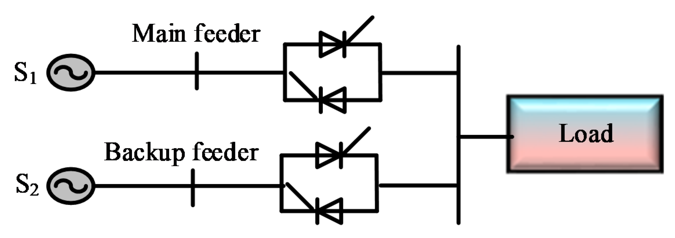
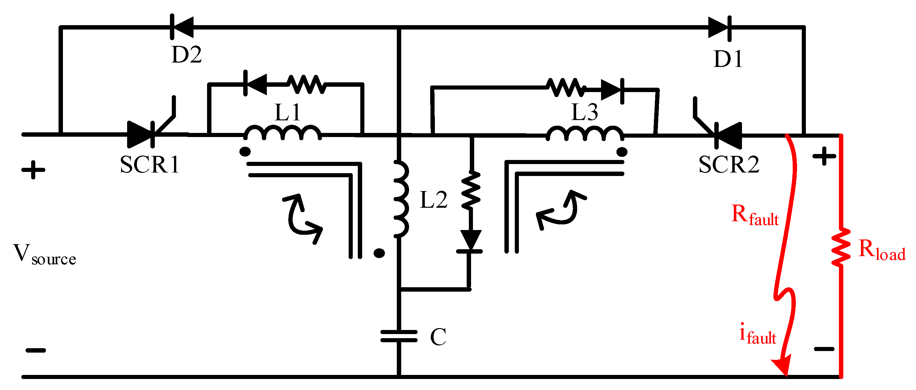
3.1. Forced Current Commutation Based SSTS in Improving Power Quality and Reliability

To ensure the superior characteristics with higher reliability, faster response time, and strong protection capability, intelligent microprocessor-based forced current commutation technique has been studied in [1]. The proposed topology is presented in Figure 5 [1]. The advantage of this topology is that it can reduce the switching loss, and has the characteristics of high reliability, low loss, and fast switching, which will greatly solve the problem of power supply voltage drop and instantaneous power interruption, improving the reliability of power supply and power supply quality, thus ensuring the continuity of power supply of important power places.
To explain the operation of the proposed system under normal mode, initially, the main switch remains closed keeping the alternate one disconnected. Current flows through the mechanical switching branch. Here, the resonant capacitor C is pre-charged with a certain voltage. The switching operation of the switches is reversed if any fault occurs or the voltage drop becomes too high. Again, the switching command is sent to the mechanical switch. If the contact distance of the mechanical switches comes within 2–3 mm, then the SSTS is turned ON. Inductor L and capacitor C of the LC resonant circuit generate the resonant current, which is superimposed on the mechanical switch. The SSTS is turned OFF if the mechanical switch can withstand the corresponding transient recovery voltage. During this time, metal oxide varistor (MOV) absorbs the energy of the line and the current of the main switch is reduced to zero.
Application of thyristor-based SSTS in the uninterrupted power supply has been studied in [3]. Advantage of the thyristor-based SSTS is that it can reduce the conduction loss. However, as natural commutation prolongs the overall transfer process, forced commutation technique is used in this study. Figure 6 shows the forced commutation-based transfer process of the proposed system. The rectifier is taken as a dc source to meet the demands of the inverter. In the normal grid, the loads are directly powered from the grid via the SSTS, vSSTS = 0, and SSSTS = 1, and the inverter is on standby. Once the grid fault is detected, the control unit turns off the gate-signal of the SSTS and activates the forced commutation, SSTS = 0 and FC = 1, and the inverter fast takes over the load current.
Where vSSTS and iSSTS are the voltage and the current of the SSTS, and i1, i2, and iL are, respectively, the currents of the rectifier, the inverter, and the loads. Besides, SSTS stands for the gate signals of the SSSTS, and FC is the state signals of the forced commutation.

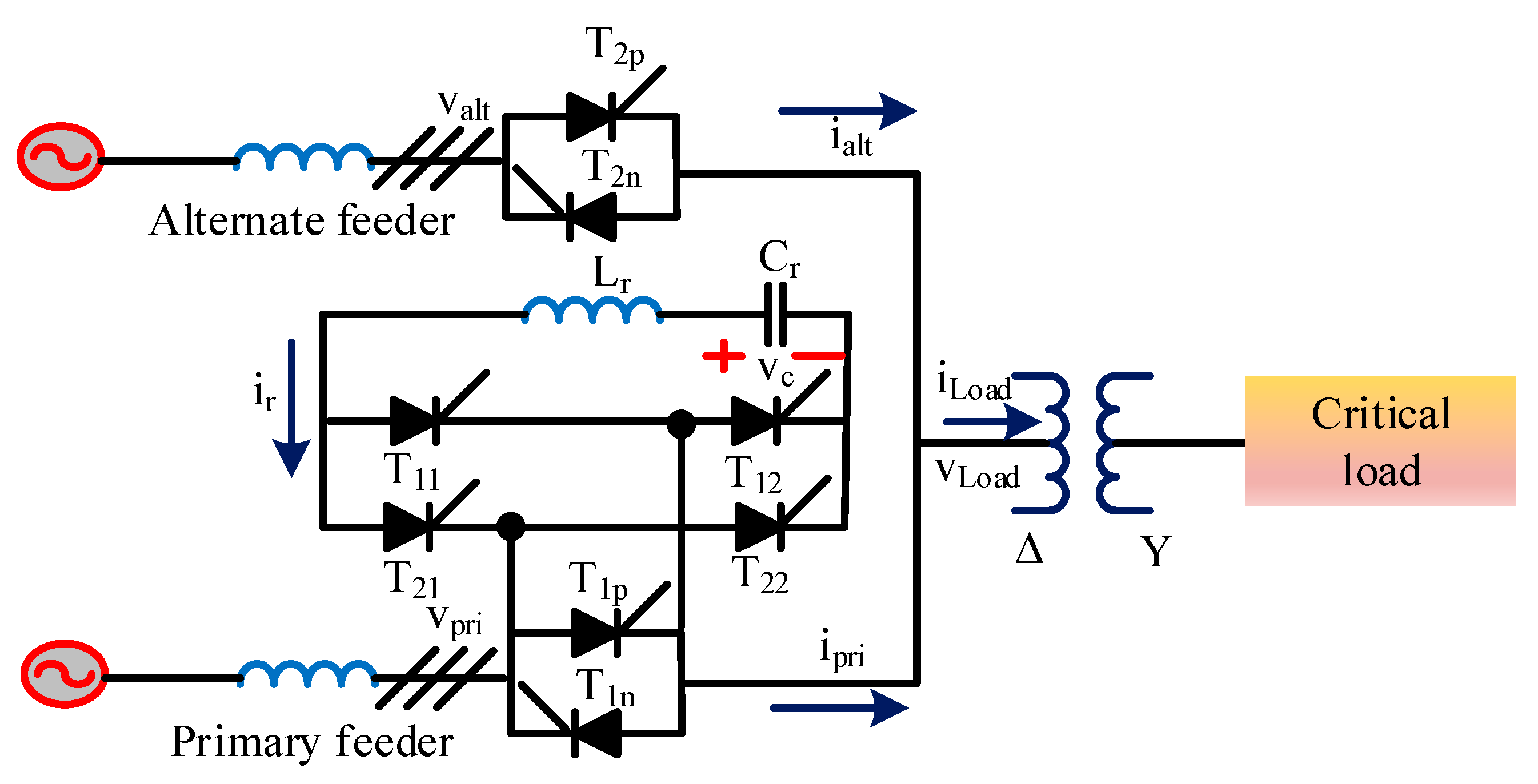
3.2. Simplified Forced Commutation Based SSTS for Commutation BRIDGE Using Flux Estimation Scheme

In [26], an impulse commutation bridge (ICB) SSTS system is proposed to further simplify the forced commutation technique (Figure 7). Using one set of LC resonant circuit in each phase, the desired outcome can be achieved. In the proposed technique, during the normal operating mode, the main thyristors—indicated as T1p, T1n, T2p, and T2n—take the overall load current, while the auxiliary thyristors (T11, T12, T21, and T22) perform this task when the forced commutation method comes into operation.
As indicated in the figure, ir denotes the resonant current. Lr (resonant inductor) is responsible for preventing the rate of rising of resonant current in auxiliary thyristors. Thus, the condition for Lr can be written as
L r V C 0 ( d i r d t | c r i t i c a l ) 1 ,
where VC0 denotes the pre-charge voltage, (dir/dt)|critical represents the critical rate of rising of the auxiliary thyristor current. After determining the inductor current, taking the stored charge Qrr as considering factor, condition for capacitor sizing (Cr) can be expressed as
C r L r 2 ( I p e a k V C 0 ) ( 1 + 1 + ( 2 L r ( Q r r I p e a k + t q ) V C 0 I p e a k ) 2 ) ,
Now, the peak resonant current ir,peak which the auxiliary thyristor must withstand during the commutation process, can be expressed by
i r   ,     p e a k I p e a k + Δ i r r ,
Δ i r r = 2 Q r r t r r = 2 Q r r d i r d t ( 1 + s ) ,
where Δirr is the reverse-recovery current, and the S is the snappiness factor of the main thyristor.
The operation of the proposed system can detect voltage sags within a quarter cycle, and then it engages the impulse commutation for fast line transfer to meet the industrial standard SEMI F47. However, the main drawback of this research is that the proposed system is not suitable for high-voltage industrial applications.

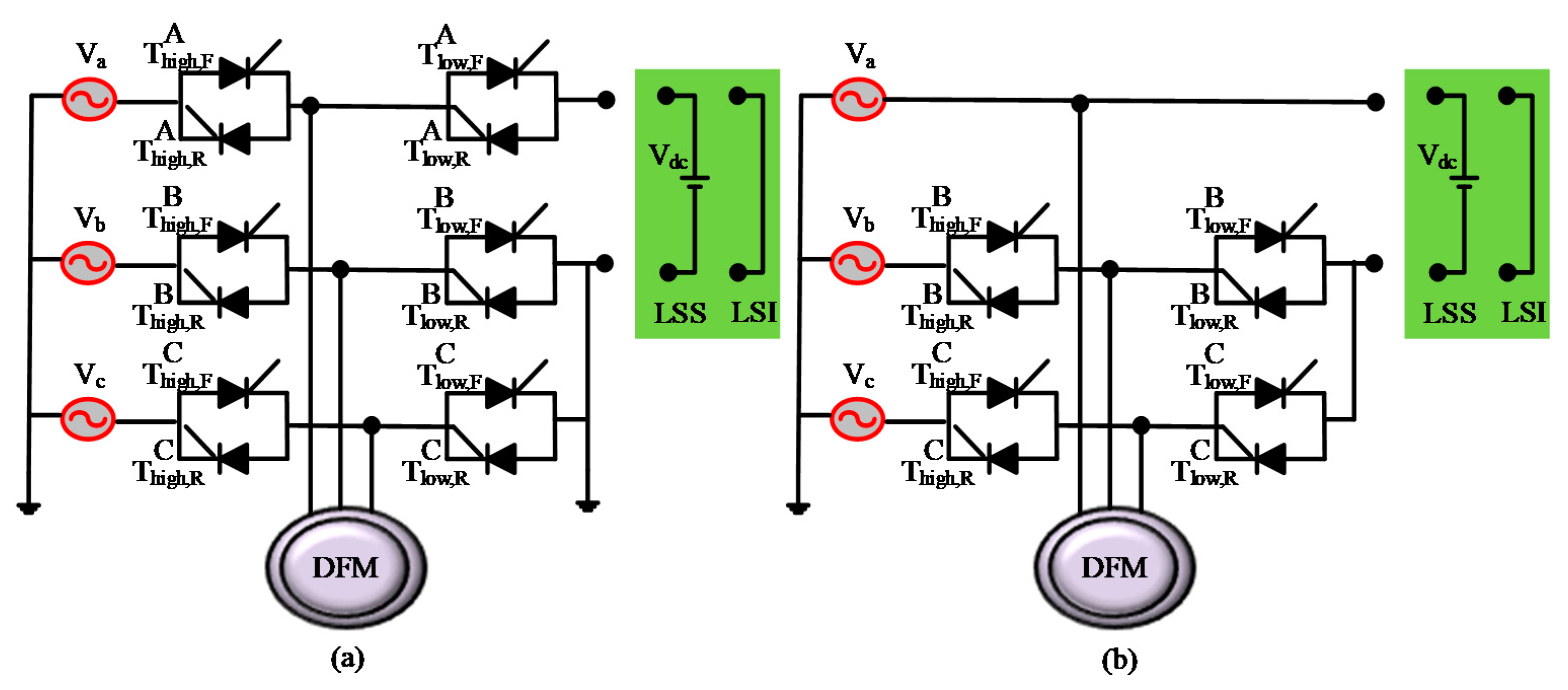
3.3. SSTS Topologies for a Switched Doubly-Fed Machine Drive

Various researches on SCR-based transfer switch topology with a different number of thyristor switches have been described in [19]. Figure 8 depicts such topology for the application in a double fed machine (DFM) where Figure 8a represents the 12-thyristor based (TTB) transfer switch that can be used in both the low-speed induction topology (LSI) and low-speed synchronous topology (LSS) topology [41]. The transfer switch topology resembles a conventional static transfer switch used in providing back-up power to critical loads from multiple ac sources [28,42]. Each of the anti-parallel SCR modules-per-phase confirms the bidirectional current carrying and bidirectional voltage blocking capability as required by the transfer switch. The SCR commutation requirements during mode transitions are based on the neutral of the ac source as the reference potential. SCR voltage rating should be sufficient to withstand the ac source phase voltages. The proposed eight-thyristor-based (ETB) transfer switch is shown in Figure 8b. According to the figure, the A phase of both the DFM and ac source voltage is connected permanently. When DFM operates in high-speed, SCRs TBhigh,F, TBhigh,R, TChigh,F, and TChigh,R are turned ON to connect the rest two phases of the DFM stator to the ac source. Each of these SCRs conducts for half of the time, corresponding to the ac source fundamental frequency. However, during the low-speed mode of operation, SCRs TBlow,F, TBlow,R, TClow,F,and TClow,R are turned ON either to connect the stator to the dc source in the LSS topology or to short them together in the LSI topology. Similarly, the B phase and C phase of the ac source also can be taken as the reference for the transfer switch operation. The future scope of this research is that it can be extended to other arrangements to provide convenient transfer switch properties for any application.

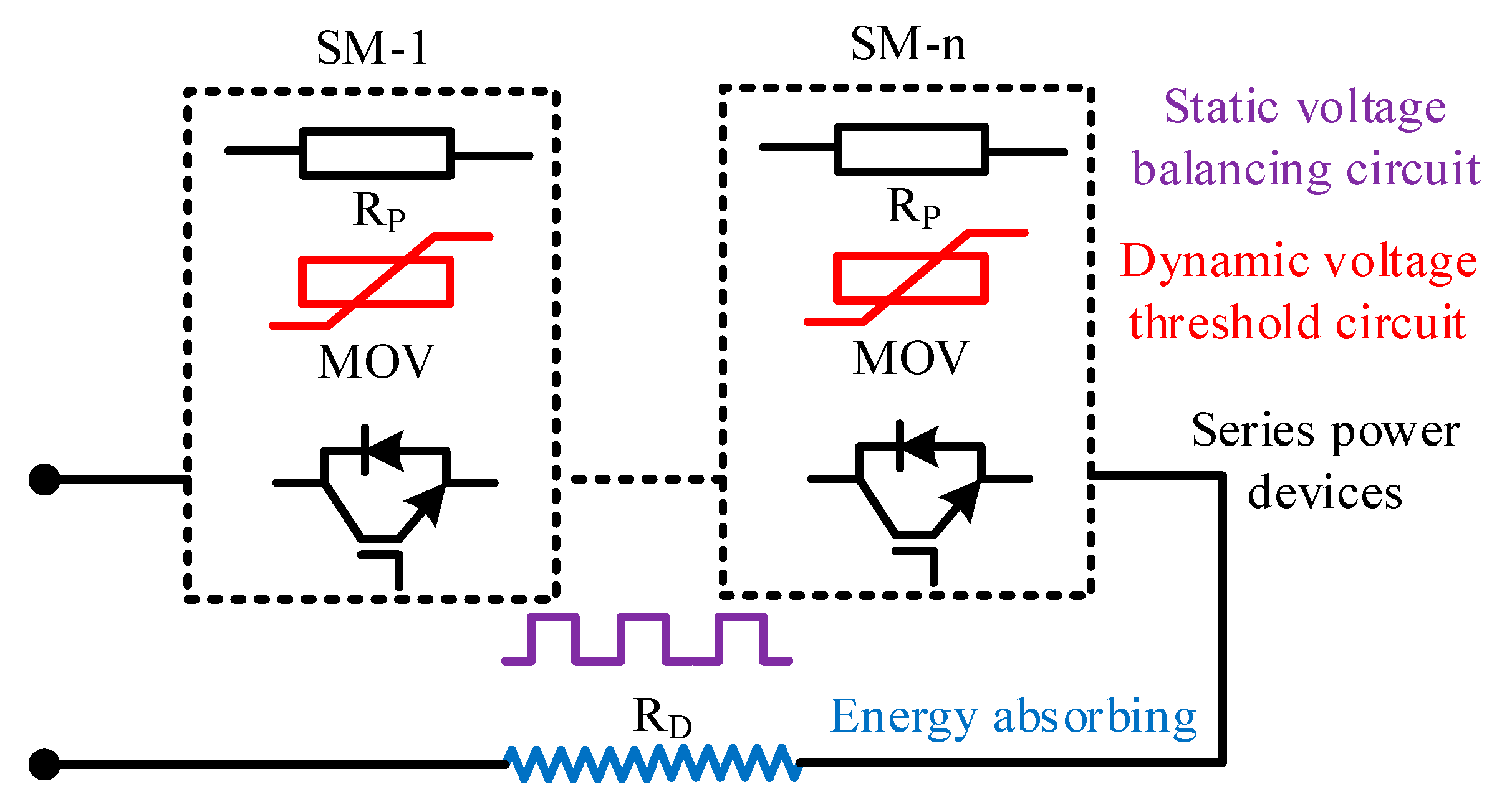
3.4. MOV-Based Modular SSTS Topologies in DC Chopper

According to [43], in case of AC chopper, the required number of semiconductor devices increases with the increase of the voltage in a wind farm, causes the serious voltage equalization problem due to the inconsistent turn-off transient process of the series-connected devices. Addressing this issue, authors in this paper proposed the modular DC chopper (DCC) which contains the fully controlled power devices. However, the reliability of the proposed method is reduced due to the use of a water-cooling system. To overcome this problem, a novel direct current chopper (DCC) with modular solid-state switches and a concentrated resistor (MC-DCC) is demonstrated in [32] for an Offshore Wind VSC-HVDC System (Figure 9).
In this research, the energy dissipation resistor (RD) adopts a concentrated design to mitigate the heat diffusion problem and replace the water-cooling system. Each submodule (SM-1 to SM-n) contains MOV and static equalizing resistor (RP) which modularize the series-connected solid-state switches [34]. With this MC-DCC system, the voltage unbalance problem in traditional DCC can be overcome as the MOV exhibits a voltage threshold characteristic, and it can effectively replace the storage DC capacitor. Moreover, the size of this proposed MC-DCC is estimated about one-half from the previous traditional modular DCCs, which further reduces the cost of the overall system with increased reliability. Study shows that the modular solid-state switches are designed such that they must turn ON and OFF continuously at a specific frequency within 1.5 s by using MOV. When switches turn OFF, the voltage threshold characteristic of the MOV turns the overvoltage of the integrated gate commutated thyristor (IGCT) under the breakdown voltage. The MOV voltage EMOV can be calculated by
E M O V = 2 T d f V r e s I s ,
where, Td represents the time for asynchronization of switches, f is the operating frequency of modular DCC, Vres and Is are the residual voltage of the MOV and operating current of the modular DCC, respectively.
However, the main drawback of this MC-DCC is that one of the solid-state switch modules fails to operate in the proposed model during a fault condition. Therefore, a dual trigger unit in the gate driver of IGCT has been proposed to mitigate the communication failure of the control system.

3.5. SSCB as SSTS to Ensure High Operating Efficiency in DC Microgrid

Considering both ac and dc microgrid system, the dc microgrid is advantageous with having better economic performance, bidirectional power flow capability and easier ‘plug and play’ operation with various distributed power generation and loads. However, there are still some issues limiting the improvement of the dc microgrid considering fault detection, isolation of failures, and arcs in fault isolation devices [44,45]. Various studies on Z-source circuit breaker are highlighted in [35]. However, these bidirectional topologies suffer from a large number of components, complex circuit structure, substantial current feedback to the source, and no common ground between the load and power supply. To mitigate those problems, a novel bidirectional dc solid-state circuit breaker is proposed in [35] to realize the bidirectional flow of energy, which ensures the higher operating efficiency of the dc microgrid (Figure 10). In this research, turn OFF time of thyristor is chosen as 50 us. The advantage of this proposed topology is that it can be applied as the protective circuit and improving the power quality.
Here, thyristor SCR1, primary coil L1 and Diode D1 constitute the forward flow of energy, wheras, thyristor SCR2, primary coil L3, diode D2 constitute the reverse flow of energy. When the fault occurs, capacitor C is discharged, current generated by the capacitor flows through the secondary coil L2 of the transformer to compensate the fault current. At the same time, the primary coil causes the thyristor current to be zero due to the mutual inductance and induced current opposite to the original current, so that the thyristor is turned OFF by the reverse voltage. The inductor voltage across L2 can be considered equal to the power supply voltage, applying KVL equation of Vsource can be expressed by
V s o u r c e = i f a u l t R f a u l t + L 2 d i f a u l t d t ,
where ifault and Rfault are the fault current and fault resistance, respectively.
To solve the above differential equation under the initial condition: t = 0, ifault = 0
i f a u l t = V s o u r c e R f a u l t ( 1 e t L 2 ) ,
Based on the first-order Taylor expansion
i f a u l t = V s o u r c e R f a u l t L 2 t   ,
From the Taylor expansion, it can be seen that the value of the fault current is proportional to the time ‘t’. When a fault occurs, capacitor C is discharged. The current generated by capacitor C flows through the secondary coil of the transformer to compensate the fault current.
Now, considering the equivalent circuit of the proposed topology, the transfer function of the input and output voltages of the circuit can be derived
V 0 V i = ( L 2 k L 1 L 2 ) C s 2 + 1 L 1 L 2 R l o a d ( 1 k 2 ) s 3 + ( L 1 + L 2 2 k L 1 L 2 ) C s 2 + L 1 R l o a d s + 1 ,
where, Vi and V0 are the input and output voltage of the equivalent circuit, k is the coupling coefficient of the two coupling coils; it is assumed the coupling resistance of the inductor is zero, which is the limitation of this study.

3.6. Commutation Based CS-MCT Evaluation to Interrupt the Fault Current in SSCB Applications

Compared with commonly used semiconductor devices, metal oxide-semiconductor (MOS)-controlled thyristor (MCT) features an ultra-low on-state resistance high surge current capability, which could be a potential candidate for SSCB applications. In [36], SSCB based on cathode-short MOS controlled thyristor (CS-MCT) has been described which can successfully interrupt the fault current for a targeted dc protection application. Corresponding results reveal that SSCB based on CS-MCT attains a 30% reduction in energy loss compared with another semiconductor device, such as insulated gate bipolar transistor (IGBT). Also, it is stated that the fault current interruption capability of SSCB can be enhanced by suppressing the mistriggering of CS-MCT. The excellent device performances coupled with the inherent reliability of solid-state power switch make CS-MCT a good candidate for future dc SSCB applications.
Figure 11 reflects the SSCB topology developed in MEDICI TCAD software. Here, Ca and La denote the pre-charged capacitor and loop inductance in commutation path, respectively. D1 acts as a free-wheeling diode, and D2 as a rectifier to avoid long-term resonance process in commutation path. In this configuration, considering the high surge current performance and inherent low turn-off capability of CS-MCT under hard-switching condition, a force commutation circuit is adopted in the SSCB to interrupt the fault current. According to this study, with a larger Ca, duration of fault current through the dc power supply will be longer, which causes a more serious electrical stress. On the other hand, a higher triggering current can also be employed to enhance the fault current interruption capability. However, this may increase the on-state resistance, leading to high power loss in SSCB. In this SSCB, both device M1 and M2 are CS-MCTs. Specifically, M1 is used to deliver a low energy loss in the main path, and M2 is adapted to provide a high current increase rate (di/dt) performance in commutation path, which is beneficial for the fast elimination of fault current through the loads. Thus, CS-MCT can be a promising candidate as a power switch in an SSCB with high energy efficiency and fault current interruption capability. However, SSCB has a large inherent on-state resistance, and hence suffers from large energy loss and finite fault interruption capability. Therefore, an advanced controlling mechanism of SSTS is required to overcome this limitation.

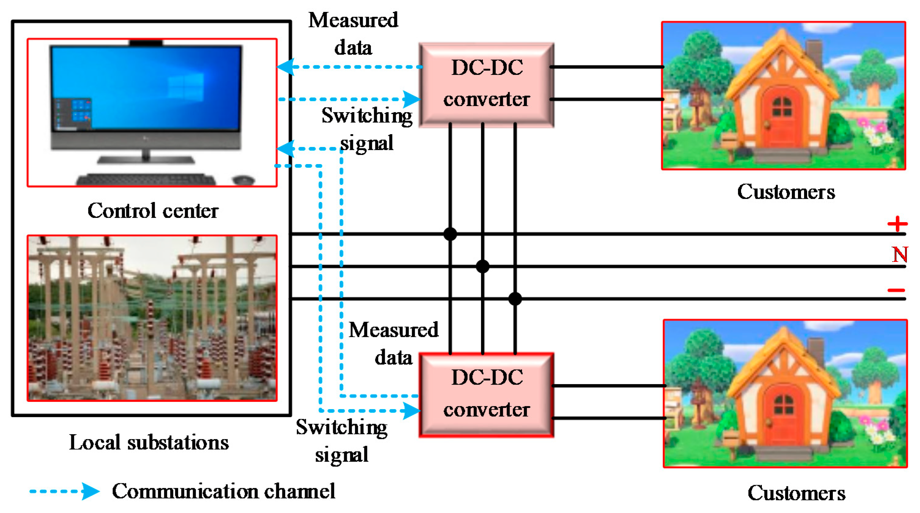
3.7. Static Load Transfer Switch in Bipolar Low Voltage DC Distribution System

Authors in [20] proposed the centralized mode of load transfer by using a static switch from a DC-DC converter. Figure 12 represents the schematic illustrating the operational concept of the static load transfer switch (SLTS) method. Here, the local substation collects the measured data from each DC-DC converter that measures voltage and current to control the internal switch in buck mode. The control center carries out decisions regarding the proper load configuration and SLTS signal generation for reconfiguring unbalanced loads. Then, SLTSs within the DC-DC converter are triggered according to the switching signal transmitted by the substation.
Figure 13 illustrates the flow diagram of the proposed method to decide the initiation of the SLTS method and to generate the control signals of the SLTSs at all load points. First, the control center, acquires load voltages and currents from DC-DC converters, which are placed at all load points. In addition, the limit of percent voltage unbalance (%VU), and the number of load points is set. Since voltage and current have a ripple component, the mean of voltage and current is calculated, and %VU at each load point is computed using the mean value. If any %VU exceeds the limit value defined by the system operator, then the value of IN and IN-k are calculated. IN and IN-k is the sum of load currents of two poles at N-th and (N-k)-th LPs, respectively.
Considering the number of load points (LPs) is equal to 3, i.e., N = 3, and k is integer (0 ≤ k < N), SLTS operation at the second LP (3-k, k = 1) is determined. Then, the trends of increasing or decreasing of neutral current are decided. In the latter case, the control signal to operate the SLTS at the second LP should be generated. Next, the same process is repeated at the first LP (3-k, k = 2). Since this computing process is repetitive, the head and tail parameters with respect to the input current of each DC-DC converter have been used, and the values of two parameters are changed according to the value of k. The current which was calculated at the first LP becomes the current of the head (Ihead), and the neutral current at the second LP becomes the current of tail (Itail). Following this, all control signals are transmitted to each DC-DC converter to operate the SLTS. The proposed SLTS method can be applicable where rapid load variations and disturbances exist. The outcome of this study reveals that additional switch gears to transfer the load connection are not required, and the neutral current with this technique also would be reduced greatly to ensure the low cost, high efficiency, and improved power quality for LVDC distribution system.

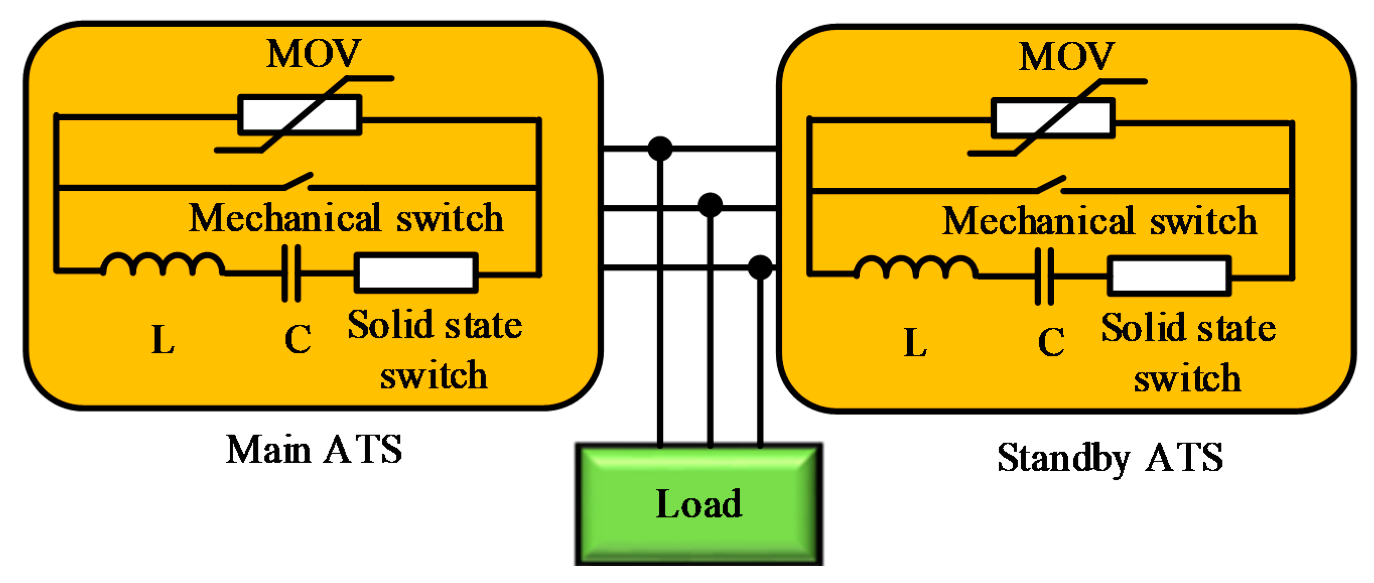
3.8. SSTS to From Hybrid ATS in Identifying the Fault Location

A 400 V/1000 kVA hybrid ATS (thyristor switch in parallel with mechanical switch) (HATS) to realize low power consumption under the normal situation with fast transfer characteristics has been proposed in [2] The proposed HATS has the contribution in realizing the overlapping transfer of the neutral wire, and deciding on source or load side transfer according to the fault locations. According to this study, conventional SSTS usually does not transfer the neutral wire, but it may not be suitable when the system contains a single-phase load. From the safety point of view for both equipment and the operator, it is not recommended to cut-off the neutral. Hence, to ensure the proper grounding, the overlapping transfer of the neutral wire is mandatory. Therefore, the faster transfer of neutral wire needs to be guaranteed in the source side.
The structure of the HATS is illustrated in Figure 14. Here, the thyristor switches, TS1 and TS2 are connected in an anti-parallel system with both the preferred source and alternate source, respectively. ATS1 is a mechanical switch with three contacts; two static contacts are connected to each source, while the moving contact is connected to the load. QS1, QS3, and QS5 are isolating switches. QS2 and QS4 are bypass switches.
The block diagram of the proposed HATS (Figure 15) consists of a voltage sag detection module, a current swell detection module, a power calculation module, a parameter management module, a decision logic module, a transfer logic module, and an event record module. The decision logic module decides the decision for transfer based on the parameters and signals given by corresponding modules. If the transfer signal given by the decision logic module is valid, the transfer logic module starts the transfer and control process. The event record module records the real-time data during the transfer process and sends the data to the host computer for further analysis. After this, a completed signal is sent to the decision logic module, and the system prepares for the next transfer.

4. SSTS Control Methods

The detailed control scheme for the operation of the SSTS has been illustrated in [18]. As shown in Figure 16, the control methods can be categorized into four parts. They are, (a) voltage detection transfer signal, (b) current direction and zero-crossing detection signal, (c) synchronizing signal, and (d) firing control logic.
This SSTS control scheme is a modification of the IEEE Benchmark STS-1 control system (IEEE PES TF 2001) where both the Park’s transformation and the three-phase PI controlled phase-locked loop (PLL) are considered. PLL is used to get the fast synchronizing and accurate firing logic signals which makes the transfer process faster.

4.1. Voltage Detection

Figure 16a depicts the voltage detection circuit where the logic depends on Park’s transformation theory. The ac system voltages are used as the input into the PLL to produce synchronizing signals which are fed into the abc to dq transformation block. The output of the transformation block (Vdq) is the voltage vector which is compared with the dc reference (Vref) to calculate the error. The error signal is then passed through a first-order low pass filter to attenuate the impact of voltage transients. The filter output is then compared to the voltage tolerance limit, VTL to determine the comparator output, which is considered as the voltage detection transfer signal. The obtained signal is used to initiate a feeder transfer process if the main feeder fails.

4.2. Current Detection

Figure 16b demonstrates the current detection and zero-crossing circuit which is responsible for turning ON/OFF the thyristor switches and selects the correct switch to trigger which further prevents the source paralleling during the transfer process. To accomplish this task, firstly, the system current is passed through the smoothing first order low pass filter, and subsequently, the output of the filter is compared with the zero current crossing threshold limit to generate the current detection signal.

4.3. PLL Synchronizing Scheme

The system voltages are fed to the three-phase PI controlled phase locked loop (PLL) as shown in Figure 16c. The aim to use the PLL is to generate the synchronizing signal (alpha value) that synchronize the voltage between the load and the feeder.

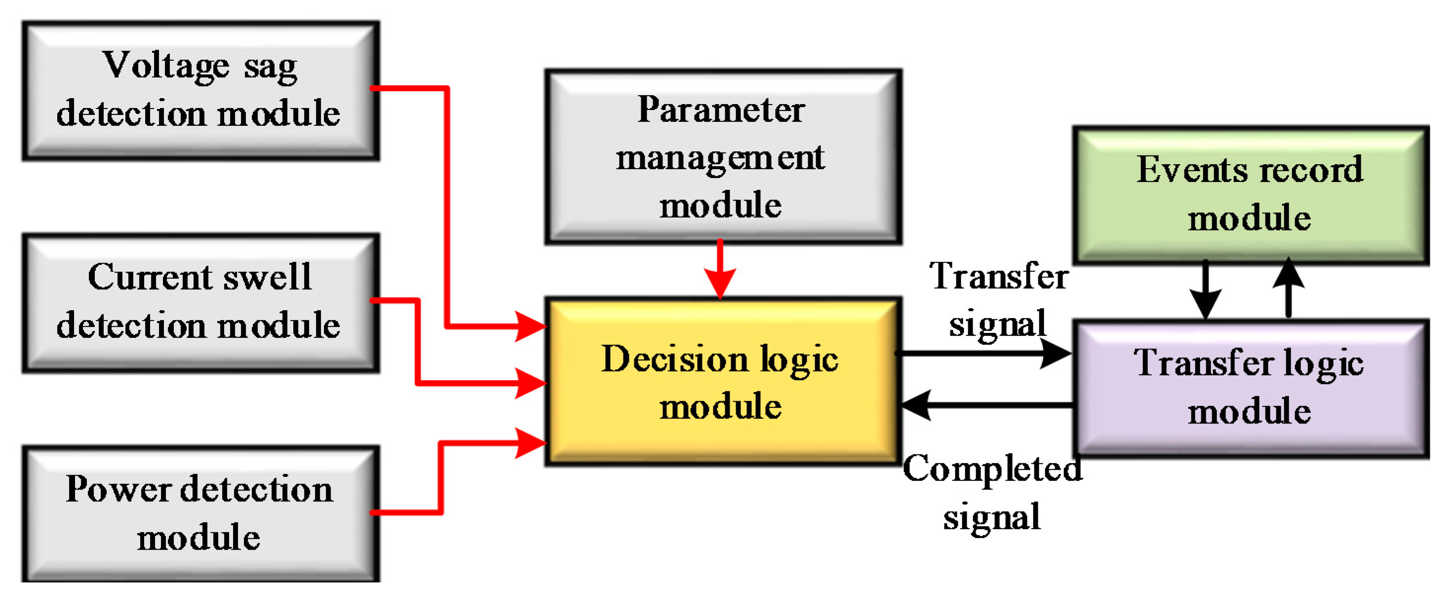
4.4. Firing Control Logic

Aiming to faster load transfer and preventing source paralleling, the switching strategy of the firing control block, as shown in Figure 16d, provides the selective switching signals to the thyristor switches depending on the current direction. The switching signals are generated for both the main and back-up feeder depending on the current direction. In case of faults in the main feeder, the thyristor switches of the main feeder are turned OFF, and thyristor switches of the back-up feeder are turned ON. If one switch of the main feeder remains conducting during the time of fault detection, one switch of the back-up feeder is gated, and the transfer process starts. If the commutation occurs and main feeder current drops below the certain limit, and back-up feeder current exceeds the zero current threshold limit, then both switches of the main feeder turned OFF and the second switch of the back-up feeder is gated. Thus, the transfer process is completed.

5. Transfer/Switching Strategies

The SSTS control system transfers the loads from the main feeder to the back-up feeder when a fault occurs. Based on the literature, two ways of transferring loads: make-before-break (MBB)/closed transition and the break-before-make (BBM)/open transition transfer process are widely available. Depending on the SSTS control method, it is possible to gate the alternate-side thyristors before the zero-current crossing on the preferred side is reached, thus allowing the alternate side to ‘force’ the preferred side to commutate (turn off). This transfer is known as a make-before-break transfer. In typical emergency systems, there is an inherent momentary interruption of power to the load when a load is transferred from one source to another. In most cases, this outage is inconsequential, particularly if less than one-sixth of a second. MBB is also known as parallel transfer or hot transfer. This strategy has gained wide acceptance because the transient on the load bus is eliminated. However, the cross-current, determined by the voltage difference between the two sources, may be very high and exceed the short-term withstand ratings of the transformers and switches, so this transfer strategy demands that two sources are in phase. The MBB strategy also satisfies the seamless transfer demand of the loads [2]. On the other hand, an SSTS can be operated to perform a ‘break-before-make’ transfer, which means that during the transfer process, the preferred and alternate sources are never paralleled. This type of transfer allows the current to go to zero in each phase of the preferred-side thyristors before the alternate side begins conducting. In this process, the electrical load will be interrupted during the shift from the normal source to the emergency source. A break-before-make switch breaks contact with one source of power before it makes contact with another with a momentary interruption of power.

5.1. MBB Transfer Strategy

The SSTS model based on MBB transfer method is proposed in [8], which consists of two modules: the voltage detection module and the transfer strategy gating module. The former is responsible for detecting the voltage sags, while the task of the latter is to execute the load transfer from the primary feeder to the alternative feeder upon detection of sag. It is shown that the longest delay caused by the MBB controller is no longer than half a cycle. Hence, MBB’s transfer time is much shorter than that of BBM’s. Successful implementation of the MBB algorithm requires accurate, current direction measurement and, consequently, proper thyristor triggering. Due to the low impedance between the two feeders, the resulting current surge can reach an unsafe level and may cause damages. This problem is defined as the cross current phenomena. Therefore, this limitation needs to be overcome by proper selection of the gating instant, tk. The following criteria are proposed to perform this task:
  • The voltage difference, Δvpa(t), in the vicinity of tk keeps decreasing, which can be expressed by
    | Δ ν p a ( n ) | > | Δ ν p a ( n + 1 ) | ,
    here Δvpa(n) and Δvpa(n + 1) are the voltage differences between two feeders, Δvpa(t), at instants t = nTss, and t = (n + 1)Tss, respectively, and Tss is the controller’s sampling time.
  • Condition for determining the upper limit of tk, (tkmax): The voltage difference, Δvpa(tk), should be smaller than the voltage difference threshold, ΔVth, which can be written as
    | Δ ν p a ( t k ) | Δ ν t h = 2 R p I c t h ( 1 e ( T s / 4 τ ) ) ,
    Here, the threshold voltage, ΔVth, is determined by the maximum allowed cross current, Icth. Here τ is the time constant, Rp is the equivalent resistance of the proposed model.
  • Condition for determining the lower limit of tk, (tkmin): The voltage difference, Δvpa(tk), needs to be larger than a certain value to allow sufficient time for successful commutation.
To ensure the successful transfer, SSTS have to possess a fired-based on the line current polarity. The polarity can be determined based on the difference between the line current and the zero-current threshold (ZCT) [46]. Study shows that SSTS performance can be improved and the cross current problem limited by enhancing the traditional make before break (MBB) strategy with the safe-triggering region (STR) approach.

5.2. Communication Strategy

To illustrate the commutation process, authors in [10] proposed an SCR-based three-phase transfer switch connected to the stator of the doubly-fed-machine (DFM) as shown in Figure 17. Two kinds of sources, one and ac, are used in this topology. The positive side of the only dc source (Vdc) is connected to A-phase, and it is then grounded by connecting all the other phases. The three ac sources (Va, Vb, and Vc) are connected in three phases, A, B, and C, respectively.

5.2.1. Transition from DC to AC Source

To accomplish the transition of the source from DC to AC, initially, the stator of DFM is assumed to be connected with the dc source. In the steady-state condition, the stator current in A phase is positive, while in the B and C phases, the stator current is negative. Taking the A-phase as a reference, a commutation diagram can be portrait as depicted in Figure 18. According to the diagram, the dashed line represents the magnitude of the dc source voltage. Prior to the transition, the stator voltage vector ( V d c ¯ , where, | V d c ¯ | = (2/3)Vdc) and the stator current vector ( I s ¯ ), both remain stationary and aligned toward the reference axis. On the other hand, the incoming ac voltage vector shows the rotating characteristics at the frequency, ωac.
Considering A phase, if the ac source voltage becomes higher than the dc voltage, the gate signal of SCR TAdc,F is turned OFF, while the firing of SCR TAac,F is activated. This condition shows by the arc PP’, which means that the ac source voltage vector must be within this arc to confirm the natural commutation of SCR TAdc,F. A similar operation is valid for B and C phases in the negative half cycle, where the arc can be represented as QQ´ and RR´, respectively.

5.2.2. Transition from AC to DC Source

In this transition, the assumption of connecting the stator of DFM is reversed, it means, the stator is assumed to be connected with ac source. The ac side SCRs (TAac,F, TAac,R, TBac,F, TBac,R, TCac,F, and TCac,R) operate on 180° conduction mode, based on the magnitude of voltage and current of the stator. In case of the A phase, when the ac source voltage becomes lower than the dc voltage, the gate signal of SCR TAac,F is turned OFF, while the firing of SCR TAdc,F is activated. The natural commutation of stator current occurs from ac to dc source. This condition shows by the arc PP´. which means that the ac source voltage vector must be within this arc to confirm the natural commutation. A similar operation is valid for B and C phases in the positive half cycle, where SCRs TBac,R and TCac,R can naturally commutate the stator current to SCRs TBdc,R and TCdc,R. The arcs can be represented as QQ´ and RR´, for B and C phases, respectively, as illustrated in Figure 19.
Table 4 concludes the characteristics of SCRs mentioning the conducting and succeeding banks at the instant of transition depending on the stator-current polarity. The angle ε in Table 4 depends upon the magnitudes of the dc- ( | V d c ¯ | ) and the ac-source voltage ( | V a c ¯ | ) vector, which can be expressed by
ε = cos 1 | V d c ¯ | | V a c ¯ |
According to the information in the table, the common requirement for simultaneous natural commutation of the ac-side SCRs is that the stator power factor angle θ must be between 120° and 240° irrespective of the location of the stator current vector. It is also seen that the complementary region of natural commutation of the conduction bank SCRs between the two-mode transitions, i.e., dc-to-ac and ac-to-dc, is due to the relative magnitude of the source voltages.

5.3. BBM Transfer Strategy

The BBM transfer strategy has been illustrated in [2]. During the transfer process of BBM, the load current had been cut off by thyristor in the preferred source, so there is no arc between the mechanical switch contacts; this is very helpful for increasing the life span of the switches. Furthermore, paralleling of the sources can be avoided strictly in this method, so it exhibits good safety to the feeders. This strategy is suitable for the loads which can endure a long transfer time (about 30–40 ms). It means the transfer process through BBM strategy is slower, which is the main limitation of this technique. BBM strategy for CMOS inverter to reduce short circuit current and power overhead has been studied in [47], where the delay is considered for low to a high transition period with NAND type edge detection technique. In this research, the time-skewed input signals are merged back into a signal output signal by this BBM process. This strategy saves 50% switching energy. The final propagation delay (TP) calculated in this study can be expressed by
T p = ( k 6 β 1 V D D + k 8 R D ) C L P + C L N 2 ,
This equation can be used to obtain the charge consumption of the transfer switch. It is noted that charge consumption has a linear relationship with propagation delay. Equation of charge consumption (Q) can be shown as
Q = 2 β 1 V D D 2 k 6 + k 8 R D β 1 V D D T p ,
where VDD id the supply voltage, RD is bidirectional relay resistor, β1 denotes the gain factor of the first stage, k6 and k8 are constants, CLP and CLN are the charging and discharging capacitive loads.
According to the study, BBM strategy is suitable for low power low precision delay elements due to its combined delay and direct path current elimination properties in one single stage. However, the transfer time of the transfer switch needs to be reduced to protect the system with improved performance and reduced cost. Hence, this strategy has limited application in the current study of the solid-state transfer switch.
Based on rigorous studies, a comprehensive review of control and switching strategies of the transfer switches has been tabulated in Table 5. It has been seen that the SSTS is mostly performed in reducing the power loss [20], overcoming the limitation of voltage sags [26,48] to improve the voltage stability [49]. Moreover, it is also observed that the hybrid transfer system is demonstrated in various studies to improve the transfer time of SSTS [2].

6. Issues and Challenges

6.1. Selection of Transfer Switch

Selecting the right transfer switch is difficult yet challenging as each installation has many variables such as switching delay, correct grounding, and neutral bonding for proper ground fault protection, contact rating/mechanical structure, maintenance, and testing with minimal power system disruption. Wrong bonding and wrong grounding in the power system can cause unwanted transients or multiple hazardous grounds based on the selection of transfer switches. Typically, when selecting a transfer switch, the main concerns are the power disturbance time versus the cost of the transfer equipment. Local authorities via standards, like the IEC 60947-6-1 standard, National Electrical Code (NEC) [56] also specify the manner of switching for particular applications. The application’s sensitivity to a power interruption during switching helps determine the transfer-switch selection. The transfer switch can be contactor or circuit breaker based, or it can be a bypass design. From less costly break-before-make switches to more expensive paralleling and synchronized transfer switches, power system protection methods must safeguard both the load and the generation system. At medium voltage, special requirements must be considered. Therefore, a transfer switch must be chosen for robust operation and maintenance at the beginning of the design process [28].

6.2. Grounding Location and Neutral Bonding

The correct arrangement of transfer switch must be chosen depending upon grounding locations and neutral bonding. Incorrect power system bonding and grounding can cause unwanted transients or multiple hazardous grounds (improper ground-fault protection) depending upon the transfer-switch selection. Improper design can create unintentional current paths and defeat ground-fault protection [28]. Hence, steps must be taken for grounding location and neutral bonding in designing the transfer switch.

6.3. Safety and Reliability

To avoid the damage of both human health and equipment, the delay in ground fault protection is not entertained. To be specific, systems with line-to-neutral loads and solid grounding, for quick operation of SSTS, ground-fault protection must be ensured [57]. Thus, human life is kept safe, and the maintenance of costly equipment are avoided. Besides, all motorized and automatic switches can also be operated manually in emergency situations and may require to be padlocked to protect it from unwanted manual or remote operations or enable safe maintenance work. It is also important to have a time delay or zero crossing detector during the transfer phenomena to check the availability of new connections. According to [16], no system is currently available which has all these safety features. On the other hand, the inclusion of transfer switch controller replacement process may improve the reliability of the transfer switch operation. Therefore, including all these features, a new generation SSTS can be designed for improved reliable SSTS operation.

6.4. Testing

Testing of the SSTS is important to check the code compliance and maintenance of the switch. The test can be of three types: integral test switch chooses the testing feature; dry contact test can be used for remote testing, and auto testing provides the monthly or annual test options to keep the record of the data in the memory. The testing does not hamper the life expectancy of the switches.

6.5. Phase Difference, Fast Commutation, and Transfer Time

Study on the impact of a phase difference between the sources of transfer switch has been studied in various researches [15]. From the literature, it was discovered that a 25° phase difference increases the load transfer time by about 2 ms. Besides, a fast commutation gating strategy also has a significant impact on reducing the transfer time where the control system does not wait for the current zero-crossing. Hence, proper adjustment of phase difference and commutation need to be adjusted for fastening the transfer process.

6.6. Memory, Materials and Costs

A memory configuration can be added with the transfer switch to keep the transfer record of the transfer switches. The memory can be interfaced with external communication tools [58]. Besides, all switches need to be designed for easy and cost-efficient installation, maintenance, and use. Modular design and smaller dimensions save precious space and significantly reducing material, handling, and installation costs.

6.7. Fault Location Identification

Fault location identification is also important because the transfer switches have to decide to transfer or not according to the different fault locations. If the fault happens on the source side, the transfer operation is required immediately, and on the other hand, if the fault occurs on the load side, the transfer operation should be forbidden. According to different load types, different phenomena will be observed to identify the fault location [2].

6.8. Uncertainties

Parameter uncertainties of switching devices have strong influence on the performance of SSTS [59]. Innovative and careful design of SSTS can result in exceptional isolation of the system, reducing the sources of random errors in the measurement path, and thus improves the measurement uncertainties of the transfer switches. Switching ratio of thermal SSTS needs to be adjusted for the application in a wide temperature range [60]. Uncertainties of the load resistance, load inductance, and load capacitance also need to be minimized by controlling the switching devices of the converter. Furthermore, SSTS should have strong fault clearing capabilities to protect the system from any mechanical or electrical damages. Although various strategies including the top-level differential protection strategy have been proposed to block the short circuit current, response time, size of SSTS, and the switching losses can further be reduced by developing the improved optimized neuro-fuzzy controlling mechanism of SSTS. However, the effect of uncertainties of the environmental impacts still have not been solved with the present existing technologies. Therefore, to obtain the combined advantages of high surge ability, strong turn-off ability to control the short circuit current, the high capability to withstand the overvoltage (according to voltage tolerance standard IEEE 1346), low weight, and increased performance of transfer switches with a faster response time under various environmental conditions, optimal hybrid SSTS topology can be a feasible solution in the future scope of small-, medium-, and large-capacity household and industrial applications.

7. Conclusions and Recommendations

This paper gives a comprehensive idea for SSTS design requirements, standards, and available specifications towards achieving the goal of mitigating the power quality issues, reducing the transfer time and losses. Available control strategies and switching mechanisms also have been discussed in this paper. From the rigorous studies on SSTS, many variations on the transfer switch are possible in different applications to reduce steady-state power consumption. Using semiconductor devices to construct the transfer switch, while allowing instantaneous transition without shorting the sources or impairing the load currents, enables significant reduction of controlled power electronics and associated passive-auxiliary components. The implementation of SSTS reduces the size of the controller, thus providing a suitable solution for low-, medium-, and high-power applications. From the analysis of the topologies, it is apparent that the magnitude and duration of the cross current can be controlled by proper timing of triggering signals, according to the voltage difference and its position. However, very few studies have been found on hybrid SSTS topologies which can reduce both the cost and transfer time. Thus, progressive research is essential to improve and implement hybrid SSTS technologies in future applications. Overall, this research can provide future researchers and industrialists with a pathway for the future development of SSTS.

Author Contributions

Conceptualization, M.A.H.; Data curation, M.F. and P.J.K.; Formal analysis, M.F.; Funding acquisition, M.A.H., P.J.K., M.S.B.A.R., M.B.M.; Investigation, M.F. and M.A.H.; Methodology, M.F. and M.S.M.; Project administration, M.A.H. and P.J.K.; Resources, M.F. and M.S.M.; Supervision, M.A.H; Validation, M.A.H and M.B.M; Visualization, M.A.H.; Writing—original draft, M.F.; Writing—review and editing, M.A.H. All authors have read and agreed to the published version of the manuscript.

Funding

This research received funded by the Tenaga Nasional Berhad under UNITEN R & D Sdn Bhd, Universiti Tenaga Nasional using grant no. U-TD-RD-19-20.

Conflicts of Interest

Authors declare no conflict of interest.

References

  1. Lu, Q.; Zhanqing, Y.; Tianyu, W.; Zhengyu, C.; Bin, L.; Rong, Z. Study on the operating characteristics of a compound automatic transfer switch based on forced current commutation. J. Eng. 2019, 2019, 3329–3332. [Google Scholar] [CrossRef]
  2. Tian, B.; Mao, C.; Lu, J.; Wang, D.; He, Y.; Duan, Y.; Qiu, J. 400 V/1000 kVA hybrid automatic transfer switch. IEEE Trans. Ind. Electron. 2013, 60, 5422–5435. [Google Scholar] [CrossRef]
  3. Tsai, M.-J.; Shen, Y.-Y.; Zhou, J.; Cheng, P.-T. A forced commutation method of the solid-state transfer switch in the uninterrupted power supply applications. IEEE Trans. Ind. Appl. 2020, 56, 1609–1617. [Google Scholar] [CrossRef]
  4. Wan, X.; Gan, Y.; Zhang, F.; Yu, Y.; Yuan, H.; Wang, H.; Zhao, C. Design of a Medium Voltage AC Fast Solid-State Transfer Switch. In Proceedings of the 2019 IEEE 10th International Symposium on Power Electronics for Distributed Generation Systems (PEDG), Xi’an, China, 3–6 June 2019; pp. 1036–1402. [Google Scholar] [CrossRef]
  5. Khan, I.; Zheng, J.; Koval, D.; Dinavahi, V. Impact of Manual Versus Automatic Transfer Switching on the Reliability Levels of an Industrial Plant. In Proceedings of the Conference, 2004 IEEE Industrial and Commercial Power Systems Technical, Clearwater Beach, FL, USA, 1–6 May 2004; Volume 41, pp. 109–115. [Google Scholar] [CrossRef]
  6. Hashim, M.H.; Megat Rasidin, M.A.F.; Adullah, S. Automatic Transfer Scheme (ATS) Experience in Tenaga Nasional Berhad Distribution Negeri Perak. 2008. Available online: http://dspace.unimap.edu.my/123456789/15688 (accessed on 3 August 2020).
  7. Urciuoli, D.P.; Ibitayo, D.; Koebke, G.; Ovrebo, G.; Green, R. A Compact 100-A, 850-V, Silicon Carbide Solid-State DC Circuit Breaker. In Proceedings of the 2016 IEEE Energy Conversion Congress and Exposition (ECCE), Milwaukee, IL, USA, 18–22 September 2016; pp. 1–5. [Google Scholar] [CrossRef] [Green Version]
  8. Yao, J.; Abramovitz, A.; Wang, Y.; Weng, H.; Zhao, J. Safe-triggering-region control scheme for suppressing cross current in static transfer switch. Electr. Power Syst. Res. 2015, 125, 245–253. [Google Scholar] [CrossRef]
  9. Mazumdar, J. Application of Transfer Switch in Mining Converters. In Proceedings of the 2010 IEEE Industry Applications Society Annual Meeting, Houston, TX, USA, 3–7 October 2010; pp. 1–5. [Google Scholar] [CrossRef]
  10. Banerjee, A.; Chang, A.H.; Surakitbovorn, K.N.; Leeb, S.B.; Kirtley, J.L. bumpless automatic transfer for a switched doubly-fed machine propulsion drive. IEEE Trans. Ind. Appl. 2015, 51, 1. [Google Scholar] [CrossRef]
  11. Sannino, A. Power Quality Improvement in an Industrial Plant with Motor Load by Installing a Static Transfer Switch. In Proceedings of the Conference Record of the 2001 IEEE Industry Applications Conference. Proc of the IEEE t36th IAS Annual Meeting, Chicago, IL, USA, 30 September–4 October 2001; Volume 2, pp. 782–788. [Google Scholar]
  12. He, N.; Shuai, Z.; Lei, Z.; Wang, W.; Yang, X.; Shen, Z.J. A SiC JFET-based solid state circuit breaker with digitally controlled current-time profiles. IEEE J. Emerg. Sel. Top. Power Electron. 2019, 7, 1556–1565. [Google Scholar] [CrossRef]
  13. Palav, L.; Gole, A.M. On Using the Solid State Breaker in Distribution Systems. In Proceedings of the IEEE Canadian Conference on Electrical and Computer Engineering, Waterloo, ON, Canada, 25–28 May 1998; Volume 2, pp. 693–696. [Google Scholar]
  14. Mische, W.; Stevens, R.A.; Lee, J.J.; MacGregor, M. US010491036B1: Solid-State Automatic Transfer Switch. Patent number 10491036, 26 November 2019. [Google Scholar]
  15. Mokhtari, H.; Iravani, M.R. Effect of source phase difference on static transfer switch performance. IEEE Trans. Power Deliv. 2007, 22, 1125–1131. [Google Scholar] [CrossRef]
  16. Hermans, L. Emergency Power Transfer Switch System. U.S. 2019/0067990; Application No. 16/111678, 28 February 2019. [Google Scholar]
  17. Da Silva, D.J.; Ventura, J.; Amaral, J.S.; Amaral, V.S. Enhancing the temperature span of thermal switch-based solid state magnetic refrigerators with field sweeping. Int. J. Energy Res. 2018, 43, 742–748. [Google Scholar] [CrossRef]
  18. Hannan, M.A.; Mohamed, A.; Hussain, A. A simulation model of solid-state transfer switch for protection in distribution systems. J. Appl. Sci. 2006, 6, 1993–1999. [Google Scholar] [CrossRef] [Green Version]
  19. Banerjee, A.; Leeb, S.B.; Kirtley, J.L.; Leeb, S. Solid-state transfer switch topologies for a switched doubly fed machine drive. IEEE Trans. Power Electron. 2015, 31, 5709–5720. [Google Scholar] [CrossRef]
  20. Gwon, G.-H.; Kim, C.-H.; Oh, Y.-S.; Noh, C.-H.; Jung, T.-H.; Han, J. Mitigation of voltage unbalance by using static load transfer switch in bipolar low voltage DC distribution system. Int. J. Electr. Power Energy Syst. 2017, 90, 158–167. [Google Scholar] [CrossRef]
  21. Langston, J.; Hauer, J.; Leonard, I.; Sloderbeck, M.; Steurer, M.; Dalessandro, D.; Fikse, T.; Borraccini, J. Demonstration of Solid State Circuit Breakers within Low Voltage DC Distribution System for Shipboard Applications. In Proceedings of the 2019 IEEE Electric Ship Technologies Symposium (ESTS), Arlington, VA, USA, 13–16 August 2019; pp. 460–467. [Google Scholar] [CrossRef]
  22. Niaki, S.A.N.; Fard, S.H. US010312684B2: System and Method for Intelligent Static Transfer Switch with Smart Home Power Management. Patent number 20190237970, 1 August 2019. [Google Scholar]
  23. Zhang, X.; Yu, Z.; Zhao, B.; Chen, Z.; Lv, G.; Huang, Y.; Zeng, R.; Lyu, G. A novel mixture solid-state switch based on igct with high capacity and IGBT with high turn-off ability for hybrid DC breakers. IEEE Trans. Ind. Electron. 2020, 67, 4485–4495. [Google Scholar] [CrossRef]
  24. Chen, Z.; Yu, Z.; Zhang, X.; Wei, T.; Lyu, G.; Qu, L.; Huang, Y.; Zeng, R. Analysis and experiments for IGBT, IEGT, and IGCT in hybrid DC circuit breaker. IEEE Trans. Ind. Electron. 2018, 65, 2883–2892. [Google Scholar] [CrossRef]
  25. Zhang, X.; Yu, Z.; Chen, Z.; Zhao, B.; Zeng, R. Optimal Design of Diode-Bridge Bidirectional Solid-State Switch Using Standard Recovery Diodes for 500-kV High-Voltage DC Breaker. IEEE Trans. Power Electron. 2020, 35, 1165–1170. [Google Scholar] [CrossRef]
  26. Cheng, P.-T.; Chen, Y.-H. Design of an impulse commutation bridge for the solid-state transfer switch. IEEE Trans. Ind. Appl. 2008, 44, 1249–1258. [Google Scholar] [CrossRef]
  27. UL Standards. UL Standard For Transfer Switch Equipment, 8th ed.; UL Standards: Northbrook, IL, USA, 2014; No. 1008. [Google Scholar]
  28. Ransom, D.L. Choosing the correct transfer switch. IEEE Trans. Ind. Appl. 2013, 49, 2820–2824. [Google Scholar] [CrossRef]
  29. William, P.; Risko, P.W. Considerations Involving the Application of Medium Voltage Subcycle Static Transfer Switches. EE Online Magazine 2002, 4, 1–3. [Google Scholar]
  30. IEC. LVDC: Electricity for the 21st century; International Electrotechnical Commission: Geneva, Switzerland, 2002. [Google Scholar]
  31. Comtech EF Data. RRS11: Solid-State Transfer Switch Installation and Operation Manual; Comtech EF Data: Tempe, AZ, USA, 2010. [Google Scholar]
  32. Xu, C.; Zhang, X.; Yu, Z.; Zhao, B.; Chen, Z.; Zeng, R. A Novel DC chopper with MOV-based modular solid-state switch and concentrated dissipation resistor for ±400 kV/1100 MW offshore wind VSC-HVDC system. IEEE Trans. Power Electron. 2020, 35, 4483–4488. [Google Scholar] [CrossRef]
  33. Nova Electric. Available online: https://novaelectric.com/wp-content/uploads/2014/01/Jupiter-Series-10-100-KVA-120-VDC-Pure-Sine-Wave-DC-AC-Inverters.pdf (accessed on 3 August 2020).
  34. Zhang, X.; Yu, Z.; Chen, Z.; Huang, Y.; Zhao, B.; Zeng, R. Modular design methodology of dc breaker based on discrete metal oxide varistors with series power electronic devices for HVdc application. IEEE Trans. Ind. Electron. 2019, 66, 7653–7662. [Google Scholar] [CrossRef]
  35. Wang, Y.; Li, W.; Wu, X.; Wu, X. A novel bidirectional solid-state circuit breaker for DC microgrid. IEEE Trans. Ind. Electron. 2018, 66, 5707–5714. [Google Scholar] [CrossRef]
  36. Chen, W.; Li, Z.; Zhang, B.; Tao, H.; Liu, C.; Xia, Y.; Shi, Y.; Liu, Y.; Liu, C.; Liu, J.; et al. Evaluation of CS-MCT in DC solid-state circuit breaker applications. IEEE Trans. Ind. Appl. 2018, 54, 5465–5473. [Google Scholar] [CrossRef]
  37. Comtech. Available online: https://www.comtechefdata.com/files/datasheets/ds-STS11_STS11L.pdf (accessed on 3 August 2020).
  38. LayerZero Power Systems Inc. LayerZero eSTS Static Transfer Switch. Available online: https://www.layerzero.com/Products/Static-Transfer-Switches/index.html (accessed on 3 August 2020).
  39. Socomec Innovative Power Solution. Transfer Switches; Socomec Innovative Power Solution: Archdale, NC, USA, 2001. [Google Scholar]
  40. Eaton. Cutler-Hammer Transfer Switches. Available online: https://www.eaton.com/ecm/groups/public/@pub/@eatonca/@elec/documents/content/pct_1606533.pdf (accessed on 3 August 2020).
  41. Banerjee, A.; Leeb, S.B.; Kirtley, J.L. Transient Performance Comparison of Switched Doubly-Fed Machine Propulsion Drives. In Proceedings of the 2015 IEEE Transportation Electrification Conference and Expo (ITEC), Dearborn, MI, USA, 14–17 June 2015; pp. 1–6. [Google Scholar]
  42. Liu, Z.; Liu, J. Indirect current control based seamless transfer of three-phase inverter in distributed generation. IEEE Trans. Power Electron. 2013, 29, 3368–3383. [Google Scholar] [CrossRef]
  43. Maneiro, J.; Tennakoon, S.; Barker, C.; Hassan, F.; Hassan, F. Energy Diverting Converter Topologies for HVDC Transmission Systems. In Proceedings of the IEEE 2013 15th European Conference on Power Electronics and Applications (EPE), Lille, France, 2–6 September 2013; pp. 1–10. [Google Scholar]
  44. Weilin, L.; Liang, L.; Liu, W.; Wu, X. State of charge estimation of lithium-ion batteries using a discrete-time nonlinear observer. IEEE Trans. Ind. Electron. 2017, 64, 8557–8565. [Google Scholar] [CrossRef]
  45. Ding, X.; Du, M.; Duan, C.; Guo, H.; Xiong, R.; Xu, J.; Cheng, J.; Luk, P.C.-K. Analytical and experimental evaluation of SiC-inverter nonlinearities for traction drives used in electric vehicles. IEEE Trans. Veh. Technol. 2018, 67, 146–159. [Google Scholar] [CrossRef]
  46. Mahmood, T.; Choudhry, M.A. Application of State Estimation Technique for Impedance Matching to Optimize Static Transfer Switch operation. In Proceedings of the IEEE 2007 International Conference on Emerging Technologies, Islamabad, Pakistan, 12–13 November 2007; pp. 269–273. [Google Scholar]
  47. Puhan, J.; Raič, D.; Tuma, T.; Árpád, B. Break-before-make CMOS inverter forp power-efficient delay implementation. Sci. World J. 2014, 2014, 1–12. [Google Scholar] [CrossRef] [Green Version]
  48. Moschakis, M.; Hatziargyriou, N. A detailed model for a thyristor-based static transfer switch. IEEE Trans. Power Deliv. 2003, 18, 1442–1449. [Google Scholar] [CrossRef] [Green Version]
  49. Cañizares, C.A.; Cavallo, C.; Pozzi, M.; Corsi, S. Comparing secondary voltage regulation and shunt compensation for improving voltage stability and transfer capability in the Italian power system. Electr. Power Syst. Res. 2005, 73, 67–76. [Google Scholar] [CrossRef]
  50. Mokhtari, H.; Dewan, S.; Iravani, M. Effect of regenerative load on a static transfer switch performance. IEEE Trans. Power Deliv. 2001, 16, 619–624. [Google Scholar] [CrossRef]
  51. Anaya-Lara, O.; Acha, E. Modeling and analysis of custom power systems by PSCAD/EMTDC. IEEE Trans. Power Deliv. 2002, 17, 266–272. [Google Scholar] [CrossRef]
  52. Mokhtari, H.; Dewan, S.; Iravani, M. Analysis of a static transfer switch with respect to transfer time. IEEE Trans. Power Deliv. 2002, 17, 190–199. [Google Scholar] [CrossRef]
  53. Kim, J.-H.; Ryu, M.-H.; Min, B.-D.; Shenderey, S.V.; Kim, J.S.; Rim, G.-H. High Voltage Pulse Power Supply Using Marx Generator & Solid-State Switches. In Proceedings of the 31st Annual Conference of IEEE Industrial Electronics Society, Raleigh, NC, USA, 6–10 November 2005. [Google Scholar]
  54. Wang, L.; Feng, B.; Wang, Y.; Wu, T.; Lin, H. Wang bidirectional short-circuit current blocker for DC microgrid based on solid-state circuit breaker. Electronics 2020, 9, 306. [Google Scholar] [CrossRef] [Green Version]
  55. Sannino, A. Static Transfer Switch: Analysis of Switching Conditions and Actual Transfer Time. In Proceedings of the 2001 IEEE Power Engineering Society Winter Meeting. Conference Proceedings (Cat. No.01CH37194), Columbus, OH, USA, 28 January–1 February 2001; pp. 120–125. [Google Scholar]
  56. NFPA. NFPA Codes and Standards: National Electrical Code; NFPA: Quincy, MA, USA, 2017; No. 70, Edition 2017. [Google Scholar]
  57. IEEE. IEEE. IEEE Standard Electrical Power System Device Function Numbers, Acronyms, and Contact Designations—Redline. In IEEE Standard C37.2-2008 (Revision of IEEE Standard C37.2-1996)—Redline; IEEE: Piscataway, NJ, USA, 2008; pp. 1–62. [Google Scholar]
  58. Ibrahim, M.; Siciliano, R.; Hayes, J. US009989948B2: Methods And Systems for Dynamic Memory Backup for Transfer Switch Controllers. Patent number 99899482018, 5 June 2018. [Google Scholar]
  59. Leyva-Ramos, J.; Morales-Saldana, J. Uncertainty models for switch-mode DC-DC converters. IEEE Trans. Circuits Syst. I Regul. Pap. 2000, 47, 200–203. [Google Scholar] [CrossRef]
  60. Adams, M.J.; Verosky, M.; Zebarjadi, M.; Heremans, J.P. High switching ratio variable-temperature solid-state thermal switch based on thermoelectric effects. Int. J. Heat Mass Transf. 2019, 134, 114–118. [Google Scholar] [CrossRef]
Figure 1. Schematic of ideal transfer switch in double-fed machine (DFM) [10].
Electronics 09 01396 g001
Figure 2. IEEE benchmark system STS-1 [11].
Electronics 09 01396 g002
Figure 3. Topology for fault detection in solid-state transfer switch (SSTS) [18].
Electronics 09 01396 g003
Figure 4. Requirements of the solid-state switch in hybrid circuit breaker.
Electronics 09 01396 g004
Figure 5. System scheme of ATS [1].
Electronics 09 01396 g005
Figure 6. Forced commutation topology of thyristor-based SSTS [3].
Electronics 09 01396 g006
Figure 7. One-line diagram of the ICBSTS system [26].
Electronics 09 01396 g007
Figure 8. SCR-based transfer switch topologies. (a) TTB—the neutral of the ac source voltage is the reference for the transfer switch operation; (b) ETB—A phase of the ac source is the reference for the transfer switch operation [41].
Electronics 09 01396 g008
Figure 9. MOV based modular solid-state switches and a concentrated resistor (MC-DCC) topology [32].
Electronics 09 01396 g009
Figure 10. Novel bidirectional dc circuit breaker [35].
Electronics 09 01396 g010
Figure 11. Schematic of SSCB based on CS-MCT using mixed-model simulation [36].
Electronics 09 01396 g011
Figure 12. Schematic of the static load transfer switch (SLTS) method [20].
Electronics 09 01396 g012
Figure 13. Flowchart of proposed SLTS method [20].
Electronics 09 01396 g013
Figure 14. The main circuit structure of HATS [2].
Electronics 09 01396 g014
Figure 15. Block diagram for HATS [2].
Electronics 09 01396 g015
Figure 16. Control scheme of SSTS signal (a) voltage detection; (b) current direction and zero-crossing; (c) synchronizing; (d) firing control logic [18].
Electronics 09 01396 g016
Figure 17. Schematic for three-phase SCR-based transfer switch connected to double fed machine [10].
Electronics 09 01396 g017
Figure 18. Commutation diagram during dc-to-ac source transition [10].
Electronics 09 01396 g018
Figure 19. Commutation diagram during ac-to-dc source transition [10].
Electronics 09 01396 g019
Table 1. Requirements for designing the SSTS
I. Constraints of General Requirements:
(i) Switch logic operationFunctions
Input selectionOne source needs to be select as the preferred source, and another source which will be deemed to an alternate source.
Voltage sensingDetection of undervoltage and overvoltage conditions.
Maintain the connection between a viable voltage source and critical load.
Follow the voltage level and timing setpoints.
Current sensingDetection of overcurrent, shorted and open circuit conditions in all phases and neutral for both sources
Phase and neutral transfer requirementsOrder of switching phase and neutral: (1) Failed phases OFF, (2) New neutral ON, (3) New phases ON, (4) Failed neutral OFF
Measurement, decision, and actionNoise immune and direct measurement system, digital logic switching for decision and action
AdjustmentPhase angle difference between preferred and alternate sources, overvoltage, undervoltage, overload for source, frequency detection, retransfer time to the preferred sources
(ii) ControlLamp test, reset, source selector, auto retransfer of the selector switch, control enable key switch, alarm
(iii) IndicatorSwitch status, availability of source and load, selection of preferred source
(iv) CommunicationSerial port having standard baud rate and no parity in the data, shunt trip capability
(v) Cooling requirementsFans, filters, over-temperature detection, convection cooling
II. Constraints of Environmental Requirements:
Storage temperature−40 °C to +70 °C
Operating temperature0 °C to 40 °C for cabinet operation and 0 °C to 45 °C for panel operation
Relative humidity0% to 95% (noncondensing)
Audible noiseNot greater than 55 dB outside a radius of 6 feet
Magnetic fieldsNo appreciable magnetic fields
SeismicShall be rated for installation in Seismic Zone 4.
III. Life Expectancy:
Mean time between failureMust be greater than 300,000 h of continuous operation without failure
Table 2. Standards in designing the SSTS.
Table HeadStandards
SafetyUL 1008 (Standard for transfer switch equipment) and UL924 for load control relay [16]
ElectricalNational Electrical Manufactures Association (NEMA) ICS 10, ANSI C62.41E, Low-voltage Switchgear and Control gear; Multifunction equipment; (IEC 947-6-1), National Electrical Code (NFPA 70) in collaboration with Emerge Alliance, Essential Electrical Systems for Health Care Facilities (NFPA 99), Emergency and Standby Power Systems (NFPA 110), IEEE Recommended Practice for Emergency and Standby Power Systems for Commercial and Industrial Applications (IEEE Standard 446), Fast Transient Immunity Severity Level 4 (EN61000-4-4), Surge Immunity Class 4 (EN61000-4-5), IEC Specifications for EMI/EMC Immunity (CISPR 11, IEC 1000-4-2, IEC 1000-4-3, IEC 1000-4-4, IEC 1000-4-5, IEC 1000-4-6, IEC 1000-4-8, IEC 1000-4-11), Limits and Methods of Measurement of Radio Interference Characteristics of Industrial, Scientific and Medical Equipment (EN55011).
SoftwareANSI, IEEE
Table 3. Specifications of various SSTS models.
SSTS ModelFeaturesSpecifications/Available Data
I. SSTS Model Developed/Applied for Academic Purpose
Model:
Not specified [1]
Influence of the fault on switching has been analyzed, designed for medium voltageResponse time: 2–3 ms
System capacity: 10 MVA
Rated voltage: 10 kV
Rated frequency: 50 Hz
Model:
5STP 45Q2800 [2]
Aluminum radiator is used to fix the thyristor and nature cooling system is used for cooling purpose.Rated voltage: 2800 V
Rated current: 5490 A
Designed capacity:1000 kVA
Model:
TBBQ-3-16/4P-III [2]
More common and satisfy the needs of neutral wireRated current: 1600 A
Short time withstand current:32 kA
Opening time: 17–20 ms
Closing time: 110–140 ms
Model:
5SNA 2000K452300 [23]
Although the gate driving power of IGBT is low, the complementary advantage of IGBT and IGCT can be obtained with the inverse relationship of surge capability and turn-off capability of IGBT. Voltage ability: 4.5 kV; IRMS: 2000 A; On-state voltage: 5.8 V; Surge ability: 14 kA; Turn-off ability: >13 kA; Cost: 1.6 p.u.
Model:
5SHY 42L6500 [23]
Have enhanced conductivity modulation effect and a more preferred technology for large capacity applications. IGCTs is simple, low cost and maintain a high degree of reliability and can be turned ON and OFF by gate control.Voltage ability: 6.5 kV; IRMS: 2030 A; On-state voltage: 3.8 V; Surge ability: 26 kA; Turn-off ability: 3.8 kA; Cost: 1 p.u., System capacity: 25 kV/20 kA
Diode-bridge bidirectional switch [25]IGBT based switch and cost reduced significantlySystem capacity: 500 kV/25 kA
Modular solid state switch [32]IGCT based transfer switch Voltage rating: 4.5 kV
Current rating: 2 kA
System capacity: 1100 MW
Model:
Static switch [33]
-Voltage rating: Same as AC output; Temperature: 0–50 °C; Humidity:0–95%, noncondensing; Altitude: Up to 1500 m above sea level; Communication interface: RS-232, RS-485; Frequency: 50 Hz/60 Hz
Modular transfer switch [34]Balancing circuit and series power devicesSystem capacity: 100 kV/25 kA
SCR based Bidirectional circuit breaker [35]Ensure higher operating efficiencu in dc microgridResponse time: 50 us
Voltage rating: 400 V
Current rating: 100 A
Thyristor based switch [36]30% reduction in energy loss compare to IGBT based topologyVoltage rating: 400 V
II. Commercially Developed SSTS Model
Model:
STS11(70/140 MHz)/STS11L(L-Band) Solid-State Transfer Switches [37]
IF or L-Band switching for DM240XR modulators. Easy access to connectors and LEDs. The small size makes installation easy and convenient with included bracketsPrime power: +12 VDC
Operating temperature: 0 to 50 °C, 95% humidity, non-condensing
Storage temperature: −20 °C to +40 °C, 99% humidity, non-condensing; Switch time: 50 ms maximum; IF: 20 dB; L band: 14 dB
Model:
eSTS [38]
Provides solid-state transfers between two in-phase AC sources in quarter cycles. Performs open-transition transfer as well.No. Of inputs: 2/3; No. Of poles: 3; Frequency: 50 Hz/60 Hz; Phases: 3 phases, 3 or 4 wires; Transfer time: Nominal 1/4-cycle for in-phase sources; Cooling: Convection
Model:
LX-450 [39]
Monitors voltage and controls the transfer to and from the normal and emergency sources.No. of poles: 2, 3, 4; Short circuit rating: 100 A, 200 A, 260 A, 400 A, 600 A, 800 A, 1000 A, 1250 A; Control voltage: 120 V AC; Pick up voltage: 90% of both normal and emergency source voltage; Drop out voltage: 84% of both normal and emergency source voltage; Auxiliary contact: 10 A,125/250 V AC
Model:
RRS11 [31]
Offers IF or L-Band redundancy in a simple straight forward plug and play design. Allows the user access to the online and offline ports. No external power source required.Frequency: 70/140 MHz (L-band system)
Switch time: 50 ms maximum; Prime power: +12 V DC; Operating temperature: 0 to 50 °C, 95% humidity, non-condensing; Storage temperature: −20 to +40 °C, 99% humidity, non-condensing
Model:
Cutler-Hammer Transfer Switches [40]
Sector: Commercial
Reliable, rugged, versatile, self-protected.No. Of poles: 2, 3, 4; Frequency: 50 Hz/60 Hz
Voltage rating: 120–600 V; Current rating: 30–1000 A
Fuse type: J, T, L (based on ampere rating)
System capacity: 100 kVA
Model:
P9400A
Superior performance in terms of isolation, insertion loss and return loss across a broad operating frequency range. Suitable for high-speed radio frequency and microwave switching applications. Frequency: 100 MHz to 8 GHz; Isolation (dB): 80
Insertion loss (dB): 3.5; Return loss for ON port (dB): 15; Switching speed rise/fall: 200 ns; Input power (average) (dBm): 23; Driving voltage (VDC): 5
Model:
P9400C
-Frequency: 100 MHz to 18 GHz; Isolation (dB): 80
Insertion loss (dB): 4.2; Return loss for ON port (dB): 10; Switching speed rise/fall: 200 ns; Input power (average) (dBm): 23; Driving voltage (VDC): 5
Model:
U9400A
-Frequency: 300 kHz to 8 GHz; Isolation (dB): 100; Insertion loss (dB): 3.5; Return loss for ON port (dB): 15; Switching speed rise/fall: 4/0.5 µs; Input power (average) (dBm): 29; Driving voltage (VDC): 11 to 26 V
Model:
U9400C
-Frequency: 300 kHz to 18 GHz; Isolation (dB): 90; Insertion loss (dB): 6.5; Return loss for ON port (dB): 10; Switching speed rise/fall: 5/1 µs; Input power (average) (dBm): 27; Driving voltage (VDC): 11 to 26 V
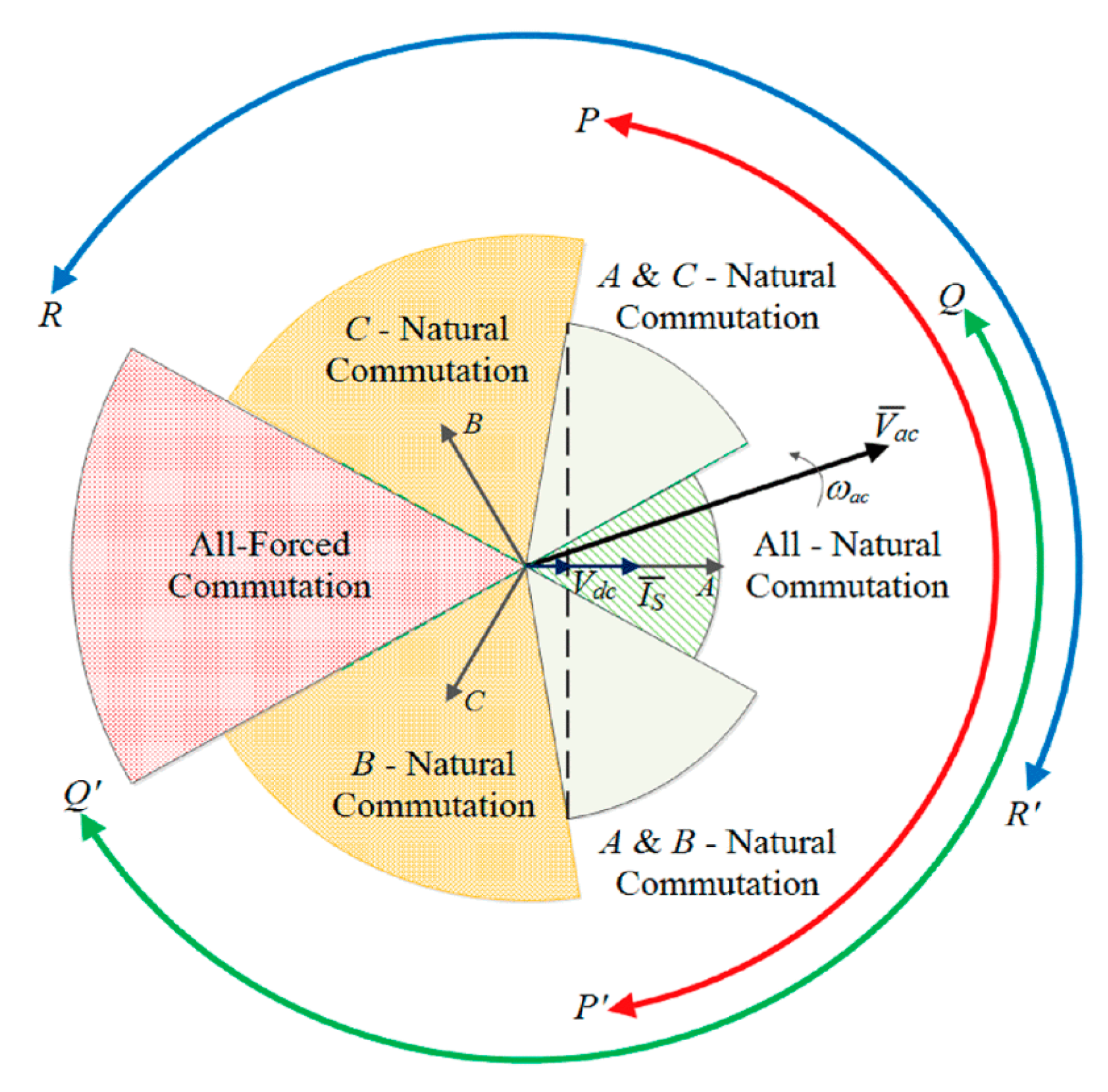
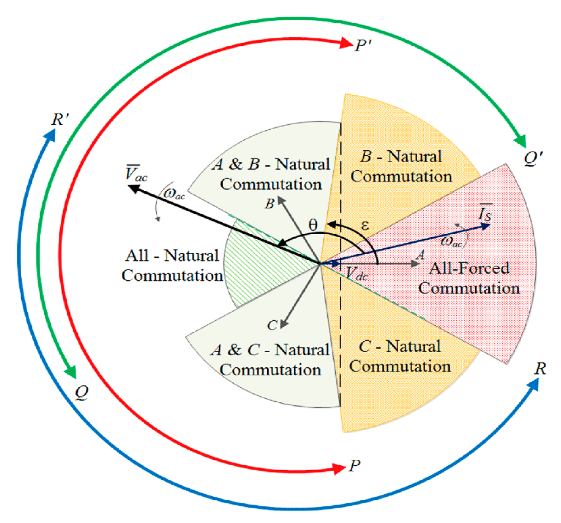
Table 4. Classification of outgoing AC-side and incoming dc side SCRs for an AC to DC source transition based on the stator current vector location
Location of Stator Current VectorConducting Bank (AC Side)Succeeding Bank (DC Side)Required AC Source Voltage Vector
−30° < I S ¯ < 30° T a c , F A , T a c , R B , T a c , R C T d c , F A , T d c , R B , T d c , R C 150° < V a c ¯ < 210°
30° < I S ¯ < 90° T a c , F A , T a c , F B , T a c , R C T d c , F A , T d c , F B , T d c , R C 210° < V a c ¯ < 360° − ε
90° < I S ¯ < 150° T a c , R A , T a c , F B , T a c , R C T d c , R A , T d c , F B , T d c , R C 360° − ε < V a c ¯ < 330°
150° < I S ¯ < 210° T a c , R A , T a c , F B , T a c , F C T d c , R A , T d c , F B , T d c , F C −30° < V a c ¯ < 30°
210° < I S ¯ < 270° T a c , R A , T a c , R B , T a c , F C T d c , R A , T d c , R B , T d c , F C 30° < V a c ¯ < ε
270° < I S ¯ < 330° T a c , F A , T a c , R B , T a c , F C T d c , F A , T d c , R B , T d c , F C ε < V a c ¯ < 150°
Table 5. Comprehensive review on SSTS control and switching strategies.
PurposeControl SchemeFeaturesRef.
Identifying the fault location and fast transfer processRealizing the overlapping transfer of neutral wire in HATSCost-effective solution for maximum power transfer reliability. Reduce the forward voltage drop of thyristors. BBM, natural communication, mechanical switch breaking the circuit and MBB strategies are possible[2]
Suppressing cross current in static switch with less than one cycle transfer time Safe-triggering region control scheme with MBB techniqueLimit the cross current surge and minimise the current stress in the system. Enhance system reliability, and it does not require any additional components.[8]
Alter the connection between ac and dc source based on speedSCR control schemeCurrent commutation of SCRs and bumpless transition in shaft behavior are both controlled from the rotor [10]
Using the solid-state breaker as a transfer switch in the distribution systemFiring logicDetect a voltage disturbance within one-fourth of a cycle. Mitigating the effect of voltage sags on sensitive loads.[13]
Reduce the power loss and mitigate voltage unbalance by using SLTSModified percent voltage unbalance system and EMTP are used.SLTS algorithm is used to determine the position of the load considering the neutral current at each load point. Reconfigure the structure of loads on the basis of data measured by a dc-dc converter[20]
Reducing voltage sagForced commutation techniqueControl the phase difference between feeder voltage
Hardware reconfiguration is difficult
[26]
Reducing voltage sagSafe gating strategyPhase voltage and line current in both feeders are of the same sign. No evaluation of the worst-case time was given[48]
Improving voltage stability and transfer capability of a transfer switchEliminate the voltage difference by adding shunt capacitorsControl the phase difference between feeder voltage
Application is difficult as hardware reconfiguration needs to match with system parameters
[49]
Effect of regenerative load on the static transfer switchVoltage detection and gating strategyCurrent direction and zero-crossing detection logic, gating pattern logic, zero voltage back up transfer logic are considered[50]
Performance evaluation of SSTSThe peak value of voltage waveformAbnormal condition is detected if the peak value exceeds the prescribed range and thyristor is activated to transfer the load to a healthy feeder[51]
Analysis of the static transfer switchPark’s transformationDoes not have an impact on the operation of the distribution system[52]
High voltage pulse power supplyVoltage balancingIGBT based 12 stages Marx generator is reduced to 3 stages[53]
Blocking the short circuit current within 4 ms in dc microgridCurrent differential protection strategyEliminate the short circuit current
Limit the overvoltage
Does not require an additional power supply
Reduce the cost and size
[54]
Analyzing the switching condition of a transfer switchMBB strategy with voltage and current conditionsWhen current direction detection errors occur, the voltage condition prevents false triggering of thyristors. The system reverts to BBM if both voltage and current conditions do not satisfy[55]

