Article

Switch Open-Fault Detection for a Three-Phase Hybrid Active Neutral-Point-Clamped Rectifier

1
Department of Electrical and Computer Engineering, Ajou University, World cup-ro 206, Yeongtong-gu, Suwon 16499, Korea
2
Department of Electronic and Electrical Engineering, Hongik University, Sejong-ro 2639, Jochiwon-eup, Sejong 30016, Korea
*
Author to whom correspondence should be addressed.
Electronics 2020, 9(9), 1437; https://doi.org/10.3390/electronics9091437
Submission received: 15 August 2020 / Revised: 31 August 2020 / Accepted: 1 September 2020 / Published: 3 September 2020
(This article belongs to the Special Issue High Power Electric Traction Systems)

Abstract

:
This paper proposes a fault-detection method for open-switch failures in hybrid active neutral-point-clamped (HANPC) rectifiers. The basic HANPC topology comprises two SiC-based metal-oxide-semiconductor field-effect transistors (MOSFETs) and four Si insulated-gate bipolar transistors (IGBTs). A three-phase rectifier system using the HANPC topology can produce higher efficiency and lower current harmonics. An open-switch fault in a HANPC rectifier can be a MOSFET or IGBT fault. In this work, faulty cases of six different switches are analyzed based on the current distortion in the stationary reference frame. Open faults in MOSFET switches cause immediate and remarkable current distortions, whereas, open faults in IGBT switches are difficult to detect using conventional methods. To detect an IGBT fault, the proposed detection method utilizes some of the reactive power in a certain period to make an important difference, using the direct-quadrant (dq)-axis current information derived from the three-phase current. Thus, the proposed detection method is based on three-phase current measurements and does not use additional hardware. By analyzing the individual characteristics of each switch failure, the failed switch can be located exactly. The effectiveness and feasibility of the proposed fault-detection method are verified through PSIM simulations and experimental results.

1. Introduction

The demands for higher efficiency and power have increased the research on topics related to power converters, in various industrial areas and energy-conversion fields [1,2,3,4]. A multilevel power converter has several advantages such as low power loss, high power output, and higher voltage capability [5,6,7,8]. Among the various multilevel converters, the three-level voltage-source converter (3-L VSC) has the advantages of bidirectional power-flow capability and low voltage stress for each switching device. The 3-L VSC uses pulse-width modulation (PWM) techniques for controlling the output power when performing DC-AC or AC-DC conversions [9,10,11,12,13,14]. A typical topology of the 3-L VSC is of a diode-clamped type, which has a clamped-diode at the neutral point of each leg. The diode neutral-point-clamped (DNPC) inverter was proposed in the 1980s; however, it has disadvantages such as the need for capacitor voltage balancing and relatively high switching losses [15]. The 3-L DNPC topology involves asymmetrical loss distribution on each power semiconductor, and thus, the switching frequency of the power converter is limited to a moderate level [12].
The DNPC-type inverter was often used to replace the clamping diodes with active switches, to overcome the uneven power loss between each switching device. Another 3-L VSC, also known as active neutral-point-clamped (ANPC), was proposed, which exhibits better performance in terms of loss distribution and lower junction temperature [16]. However, the loss distribution determination procedure requires several steps to calculate the power loss and estimate the temperature data in each switch, which increases the calculation stages and computation burdens. Instead of a complex loss distribution solution, a wide bandgap (WBG) device was adopted for next-generation power semiconductors in [17,18,19,20]. SiC is a representative candidate for WBG materials, with high voltage operation and fast electron velocity when compared to traditional silicon (Si) power devices. Additionally, the SiC devices show extremely high speeds and low losses when they change their state from on to off or vice versa. By using SiC devices, the ANPC topology is changed to a hybrid ANPC (HANPC) topology [19].
Despite the numerous merits of HANPC topology, a high probability of switch failure exists because of the increased number of switches in HANPC VSC. There is a growing interest in reliability and safety as research topics [20,21,22,23,24]. Based on industrial surveys and research conclusions, the failure of power electronics systems has been an important issue in miscellaneous applications such as vehicle dynamics and renewable energy generation. A fault is defined as a state of deviation from the standard and usual conditions. Among the power electronic components, power semiconductors are regarded as some of the weakest and most fragile parts [25] (Figure 1). For this reason, fruitful research had been conducted on switch fault diagnosis and post-fault control methods during the past few decades. However, the previous studies focused on switch faults of machine drives or three-phase (3-P) two-level rectifier systems [26,27,28].
In power semiconductors, the power loss appears as a thermal effect, such as a junction temperature change or thermomechanical stress accumulation [21,29]. As the power switch is subjected to harsh environments, the bond wires lift and cracks may be caused inside the switch, which finally result in switch failures such as an open-circuit faults [30]. The open faults disconnect the solder connections of the transistor chips and degrade the quality of the output voltage. On the other hand, a short-circuit fault causes more uncontrollable and catastrophic results such as overcurrent or overvoltage, which exceed the rated value of the electronic components [31]. Thus, a short switch fault requires instant shutting down of the power converter because a short fault can cause the entire system to collapse. Although open faults aberrate the power electronics system into unusual states, the open fault condition can be handled through special control schemes instead of applying emergency stop protocols. Therefore, many methods for open-fault detection have been studied and reported [32,33,34].
Several collaborative works on switch fault-detection methods, using neural-network techniques, have been conducted such as [35,36]. However, the neural-network approach requires learning and test processes involving large amounts of data including feature information. Therefore, online diagnosis methods are good solutions for achieving fast and intuitive outcomes of fault detection in VSCs [32]. The online diagnosis methods of transistor open-circuit faults are classified into three categories: model-based, voltage-based, and current-based methods. The model-based methods use a mathematical current model or observer model to detect an open-switch fault [31]. The voltage-based methods are based on voltage signals such as the pole voltages of the leg, pole-to-pole voltage data, DC-link voltages, or gate-signal monitoring [37]. Generally, voltage-based methods require high sampling frequencies or hardware circuits for implementation, which increase the calculation burden. The current-based methods use the phase current signals of the VSC to detect faults and identify the exact faulty switch locations [38,39,40,41,42]. The employed current information is used in a stationary reference frame or average value. There are previous fault diagnosis researches using current-based method for open fault in the DC-AC inverters such as DNPC or HANPC-type [43,44]. In the open fault of inverters, upper or lower two switches had same characteristics in the faulty condition, so the zero switching state is employed to distinguish ambiguous faulty location. But in the AC-DC rectifier, the faulty waveforms have distinctive features and a slightly different fault detection method is used. In addition to the aforementioned methodologies, other fault detection strategies using additional sensors or circuits have also been proposed; these methods provide simple processes but involve additional cost and maintenance problems [45,46,47].
In this paper, an open-switch fault detection method is introduced for HANPC rectifier systems. The proposed detection method utilizes direct-quadrant (dq) axis currents on a stationary reference frame, and are derived using a coordinate transform. When an open fault occurs in a single switching device, a distortion is produced in the dq current signal. However, the current distortion alone is not sufficient to identify the faulty location in a 3-P HANPC rectifier. Additional switching state injection is necessary to resolve ambiguous diagnosis results. Several simulation and experimental results support the effectiveness of the proposed fault detection algorithm.

2. HANPC Rectifier Comprising Si and SiC Switches

2.1. Basic Circuit Topology

The voltage and power capacities are increasing in the power electronics field [48,49]. Expanding upon the conventional topologies is not a good solution, and results in designs with excessive filter size or heat dissipation. Several studies have been conducted on the development of a superior material and novel topology such as a modular cascaded structure [50,51]. Wide-bandgap devices with high-voltage capabilities and smaller filter size and low loss characteristics, which indicates higher power density per volume and weight, are being researched in particular. SiC and GaN semiconductors are at least thrice as expensive as the same-capacity Si IGBTs because of technological difficulties. Guan et al. proposed a highly efficient power converter comprising SiC and Si switches in a leg of an ANPC inverter [20]. By combining two different switching devices, the HANPC topology takes advantage of the SiC MOSFET and competitiveness in the power converter cost.
Figure 2 presents the one-leg circuitries of DNPC, ANPC, and HANPC-type VSCs. As shown in Figure 2a, the DNPC-type VSC has two neutral-point diodes and four Si IGBTs (S1S4). The ANPC-type VSC consists of six active switches, as shown in Figure 2b. Figure 2c presents the HANPC topology, which uses SiC devices as a part of the VSC (Q1 and Q2). The remaining switches are the Si IGBTs (S1S4). The HANPC realizes good quality of loss diminution and high power-conversion efficiency despite the high-switching-frequency operation. In addition, the HANPC design is advantageous in terms of the heat dissipation and filter size because of the aforementioned features. The HANPC topology achieves equal power-loss profiles for each power transistors more easily than other types of 3-L VSCs [52]. The power-loss profile is almost the same when the HANPC inverter delivers power from DC to AC and from AC to DC. In other words, the HANPC-type rectifier converts electrical energy with higher efficiency than the DNPC or ANPC-type rectifiers.

2.2. Modulation Scheme for Si and SiC Switches

The HANPC topology uses two different modulation signals as a basic switching scheme. The two modulation signals have different frequencies: a low-speed frequency (LF) and a high-speed frequency (HF). The LF modulation signal is applied to the IGBTs to turn them on and off (~Hz), and the HF signal is used in the SiC MOSFETs as a relatively high-speed switching frequency (~kHz). As shown in Figure 3, a sinusoidal reference signal is used to generate two LF/HF modulation signals, which are implemented by a carrier-based PWM technique.
In a 3-P HANPC rectifier, first, three sine-wave reference signals (Vxs, x = a, b, c) are generated and used to calculate the offset voltage (Voffset), as presented in Figure 3a. Next, the offset voltage signal is injected into the sinusoidal reference voltage (Vxn = Vxs + Voffset) and normalized as a value of zero to one (Vxn,norm). The frequency of the LF signal is the same as that of the reference voltage, which means that, if the reference voltage is positive, the IGBT gate voltage (VGE) will be equal to the turn-on level, as presented in Figure 3c. On the other hand, the IGBT will be turned off when the reference signal is negative, and thus, the switching frequency of the IGBTs will be equal to that of the reference voltage signals. The modulation scheme for the SiC MOSFET is correlated with a triangular wave, as shown in Figure 3c. The normalized voltage reference signal (Vxn,norm) is compared with the triangular carrier wave, to determine the turning on and off of the MOSFET switches. The carrier wave repeats counting up and down its steps between zero and one band, if the normalized reference signal becomes greater than the carrier wave, in which case, the turn-on gate voltage is applied to the MOSFET. The MOSFET is turned off when the normalized voltage signal becomes smaller than the triangular wave. With carrier-based PWM, the MOSFET turns on and off at a very fast switching frequency. Figure 3d presents a 3-L output pole voltage of the HANPC, produced by applying the LF/HF modulation scheme. The value of the pole voltage oscillates between +VDC/2 (positive state, P) and 0 (zero state, O+) in a half cycle of the fundamental period; in the other half cycle, the pole voltage value oscillates between −VDC/2 (negative state, N) and 0 (zero state, O−). The switching frequency of the output pole voltage is defined as HF, which is the switching frequency of the SiC MOSFET. This implies that the HANPC topology can increase the switching frequency of the output voltage by adopting a high switching frequency in the SiC MOSFETs while the Si IGBTs operate at a lower frequency. In other words, the HANPC topology facilitates high-frequency operation easily and has high power efficiency for bidirectional operation (inverter and rectifier modes).
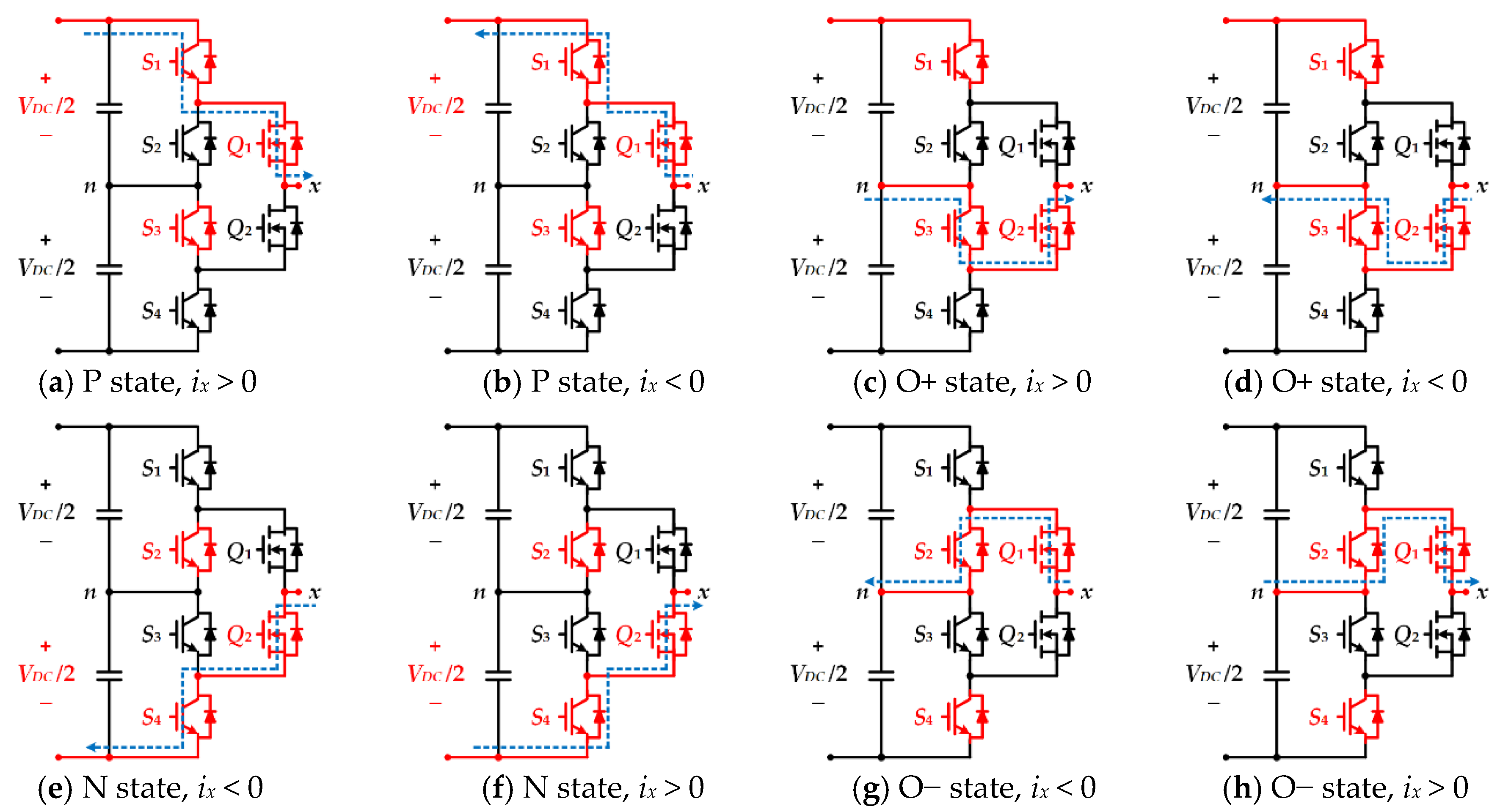
Figure 4 and Table 1 show the switching states of the HANPC topology, according to the on-off state of the transistor and direction of current conduction (ix). In a positive (P) switching state, switches S1, S3, and Q1 are turned on and the other switches are turned off, as presented in Figure 4a,b. In these cases, the output pole voltages are +VDC/2. The current conduction is differentiated by the power flows. When the switching state is P and positive current flows through the S1 transistor, active power flows from DC to AC. When negative current flows, the anti-parallel diode of switch S1 will turn on. Figure 4c,d show the zero (O+) switching state with switches S1, S3, and Q2 turned on. The HANPC-type VSC triggers the O+ state by changing only the switching state of the MOSFETs complementarily to the P state. When the switching state is the O+ state, the AC output pole (node x) is connected to the DC neutral point (node n), and the pole voltage will be 0. In this case, the MOSFET Q1 will be turned off and the Q2 switch turned on so that current flows through switches S3 and Q2. As shown in Figure 4c, positive current flows through the transistors S3 and Q2. In contrast, negative current flows through the diode part of switch S3; Figure 4d shows this current path.
Figure 4e,f indicate the negative (N) switching states of the HANPC rectifier. The N switching state generates −VDC/2 output voltage, and switches S2, S4, and Q2 are turned on. In the N switching state, the lower-side IGBT switch operates and current conducts through switches S4 and Q2; the current directions differ as shown in Figure 4e,f. As shown in Figure 4e, the current flows from the AC to the DC side, and the transistors Q2 and S4 are in the conduction mode. In the other N state (Figure 4f), current flows from the DC to the AC side, and the anti-parallel diode of switch S4 conducts electricity. Figure 4g,h present the other zero (O−) switching states, which are opposite to O+ states. In the O− states, switches S2, S4, and Q1 are turned on and the output pole is linked to the neutral point. Figure 4g depicts the switching state and current path of the O− state during negative current flow. In Figure 4h, the direction of current flow is positive and the current conduction occurs through the anti-parallel diode of the S2 switch.

3. Proposed Open-Fault Detection Method for Single Switch Failure

3.1. Feature Analysis of Switch Open Fault

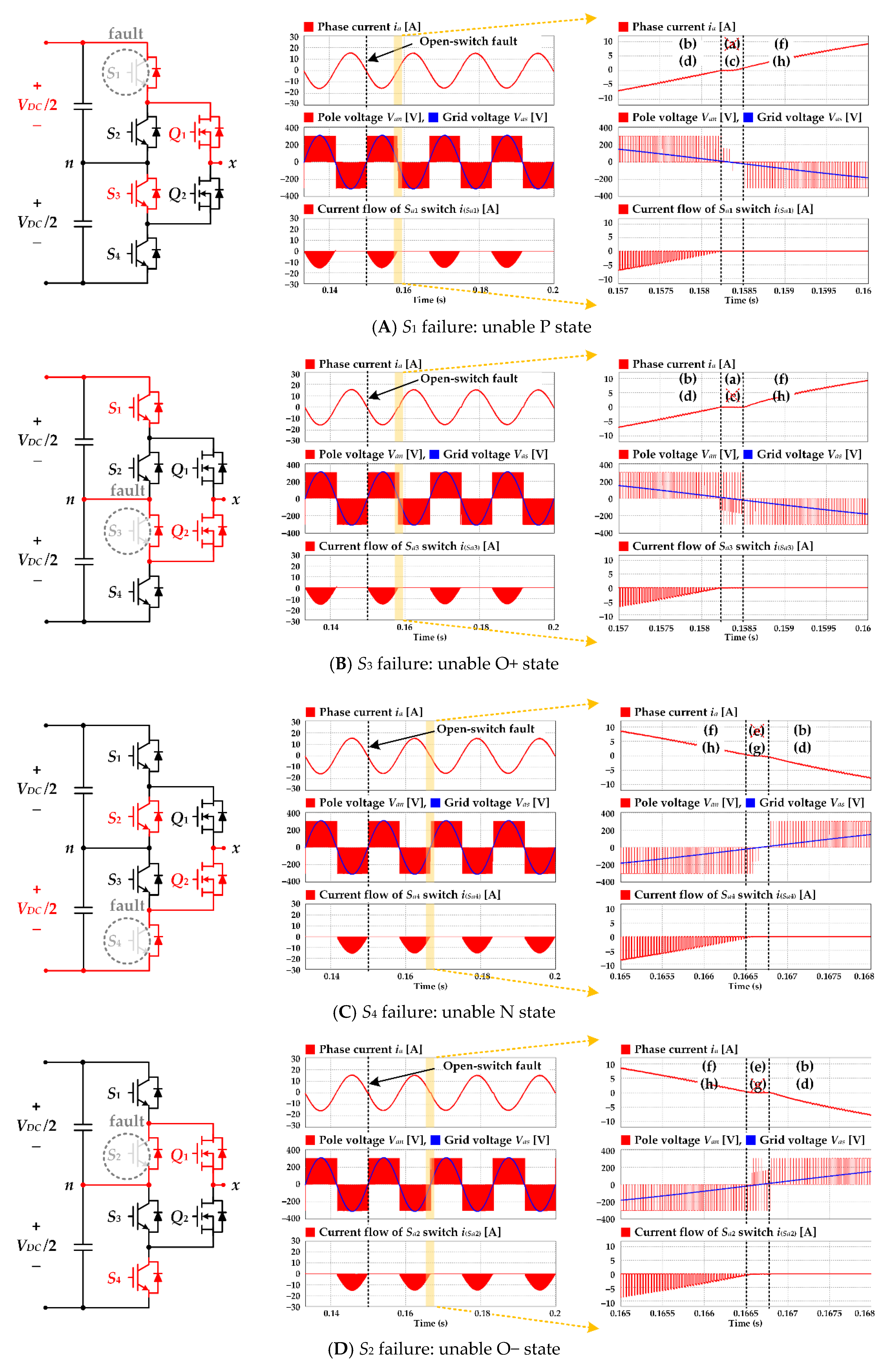
One leg of the HANPC rectifier is composed of six active switches, and the possibilities of a single open-switch failure are 18 cases in a 3-P system [43]. Figure 5 shows the phase current, output pole voltage, and AC grid voltage for each A-phase IGBT open fault (four cases). In the unity power factor condition, the open fault in the IGBT switches does not make any remarkable difference in the phase current when compared to the normal state. Figure 5A shows the case of an open-switch fault in IGBT S1. In this case, there is a short section in which the output pole voltage oscillates between +VDC/2 and 0, and the current is very small. The S1 switch fault disturbs that the faulty leg generates a P switching state in a very short time. This phenomenon is similar to the S3 open fault and is described in Figure 5B. The inner switch S3 fault blocks not to make the O+ switching state and current flows through the S3 switch. In other words, an open fault in S1 or S3 creates an open circuit and the phase current will be obstructed for a short time. Thus, the near-zero current becomes a complete zero current, because of an IGBT open-switch fault, and the so-called zero-crossing section appears.
Figure 5C shows the output pole voltage and phase current under switch S4 fault conditions. A fault in the IGBT switch S4 influences the negative current conduction when the output voltage is −VDC/2. In this section, the switching state changes between the N and O− states, as shown in Figure 4e,g. Because of an open fault in switch S4, conduction occurs as shown in Figure 4e. Similar to the S4 fault, a small current distortion occurs because of the S2 switch fault, as presented in Figure 5D. Therefore, the phase current goes to zero in the zero-crossing section; however, this section is very narrow and short when compared to the fundamental current period. This is because almost all the current flows through the diode path even though the switch fails during the AC to DC conversion.
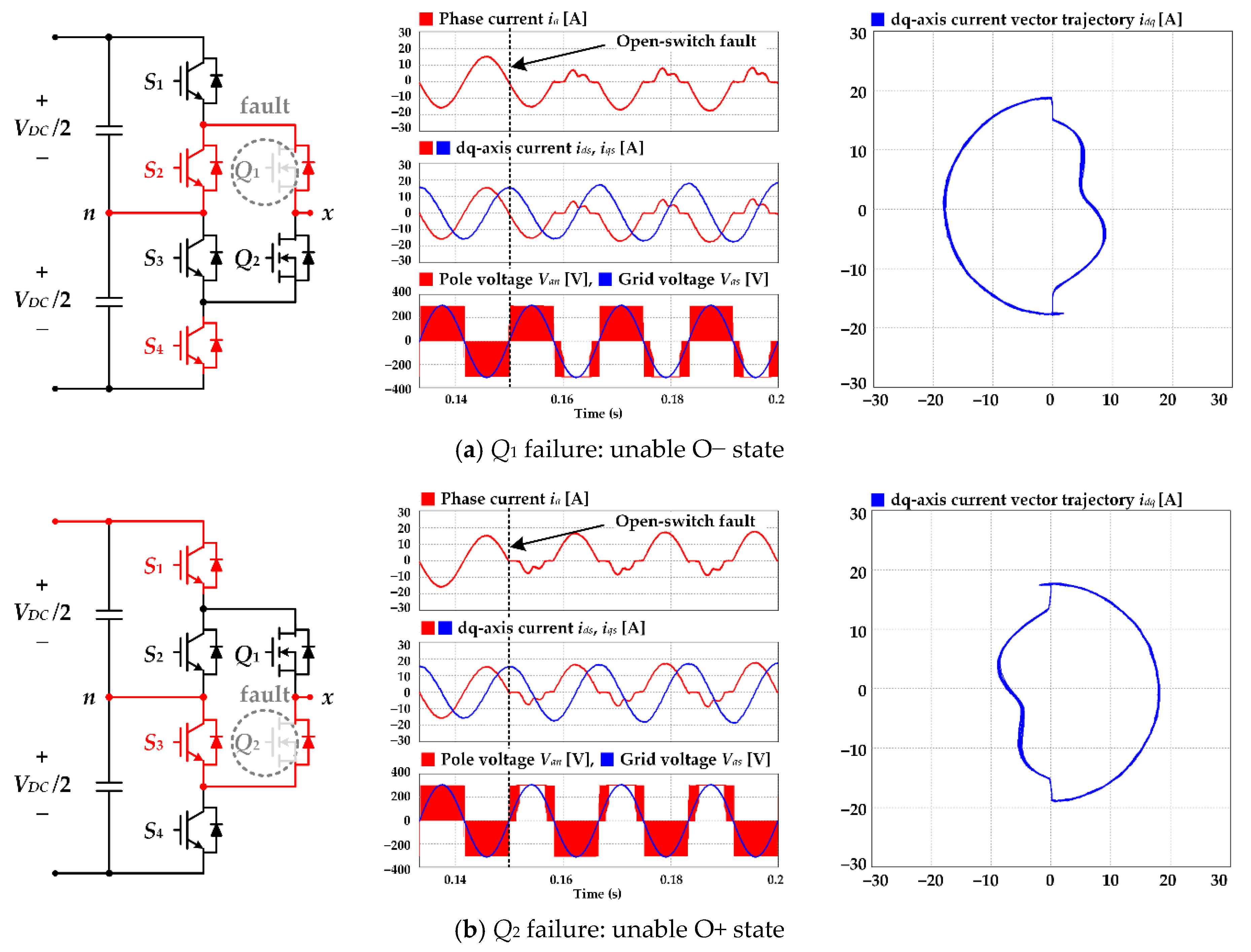
When a fault occurs in the MOSFET switches in the HANPC rectifier, the phase currents are distorted more severely. The shape of the faulty phase current deviates from a sinusoid and the zero-current section exists for a relatively longer time. As described in Figure 6, a positive or negative current does not flow as in a normal state, depending on the faulty location (upper or lower MOSFET, Q1, or Q2). The upper MOSFET Q1 fault blocks the current path in the positive current period of the fundamental cycle, and the lower side switch Q2 fault does not generate a negative current in the negative current cycle.
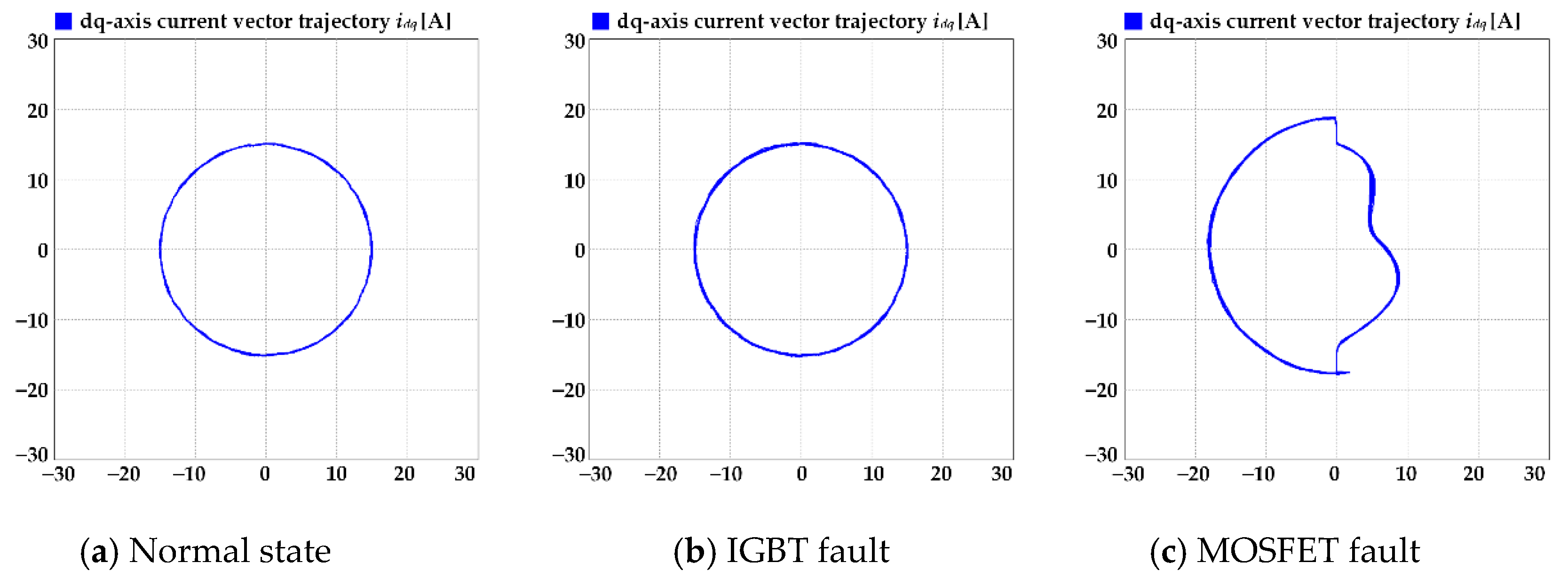
Figure 7 describes the dq-axis current vector trajectory under each condition (normal, IGBT fault, and MOSFET fault states). The vertical and horizontal axes represent the d-axis and q-axis currents, respectively, in the stationary reference frame. As shown in Figure 7b, the IGBT fault does not cause any difference from the normal state in the unity power factor condition.

3.2. Proposed Detection Method for Switch Open Fault

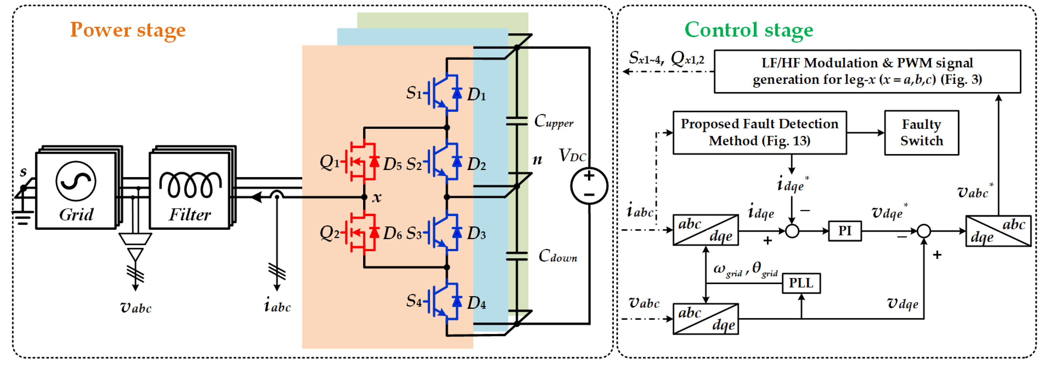
Figure 8 shows the overall control diagram for the 3-P HANPC rectifier. For grid-connected rectifier control, a phase-locked loop (PLL) algorithm is used, and a synchronous phase angle is estimated by using the 3-P voltage data [52,53,54,55,56]. Based on the estimated phase angle information, a coordination transformation is performed (Equation (1)). Using a coordination transformation (θgrid), the 3-P sinusoidal currents are converted into dq-axis currents. The dq-axis output currents are compared with the current reference signal. Next, an error is used to generate a voltage reference using a proportional integral (PI) controller [57]. Finally, PWM is performed with the voltage reference signal, and the on–off gate signals are applied to each switching device. In the synchronized dq-axis current control block, the d-axis current is used for reactive power control and q-axis current is related to active power control:
i d s = 2 i a i b i c 3 , i q s = i b i c 3
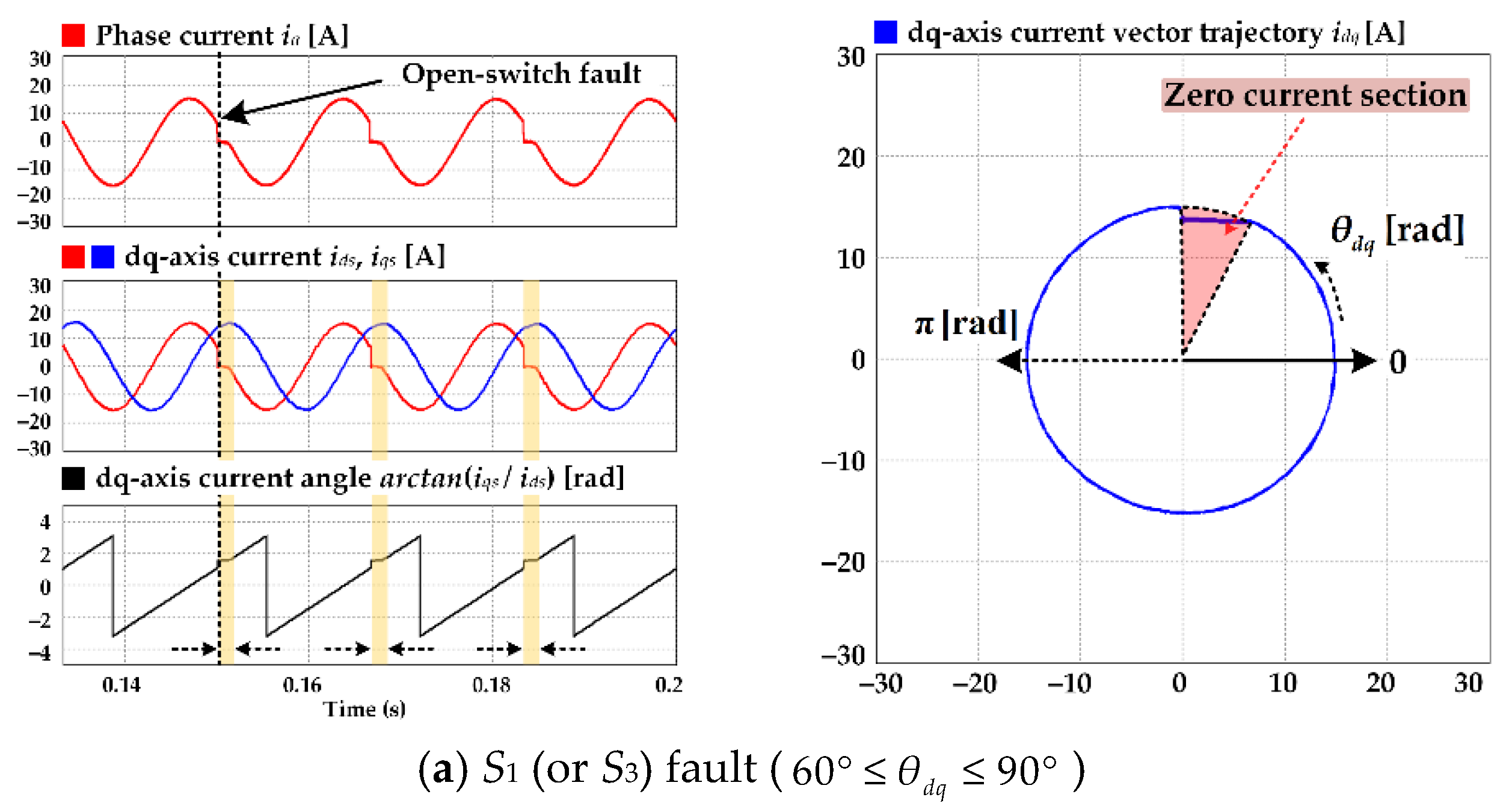
Figure 9 shows the current waveforms under the open-fault condition in each switch for the A-phase when the PF is approximately −0.7. By applying an effective value on a d-axis current (not zero), the reactive power increases, which means that the current flows through the transistor part of the IGBTs during rectification. However, the transistor path is opened because of an open fault, and the rectified phase current is clearly observed to be a zero value [58]. As presented in Figure 9, in the condition of PF = −0.7, the zero current section is longer than that during the unity PF condition. The current flows in the unity-PF condition are slightly different from those in the non-unity PF condition, and the difference is observed in the dq-axis current trajectory as well.
Figure 9 presents the Lissajous waveforms and zero-current sections under open-fault conditions for each IGBT. Some pairs have the same current shapes under a faulty condition, as shown in Figure 9a. Under the IGBT S2 and S4 fault conditions, the current waveforms are perceived to be quite similar (Figure 9b). In each case, the two open faults are similar, but there are differences in the switching states generated by the faulty leg. The dq-axis current angle (θdq) is defined as an inversion of a trigonometric function and is calculated using Equation (2) [32].
θ d q = t a n 1 ( i q s / i d s )
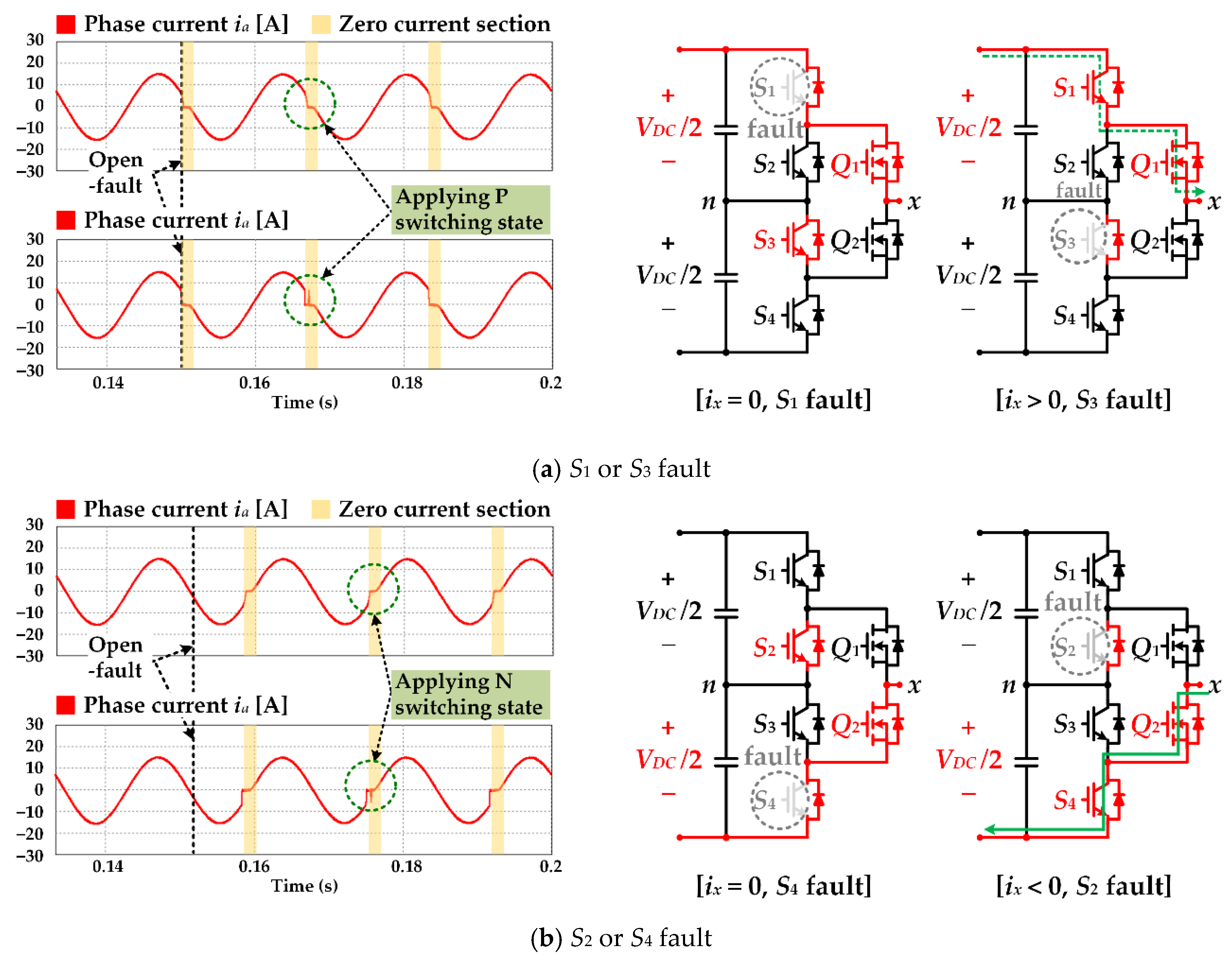
As shown in Figure 10a, when it comes to the neutral-point clamped switch S3 fault, the P switching state is possible, the positive current flows through S1, and Q1 does not conduct [43,44]. Even though the P switching state is applied, there is no current flow in the faulty leg because the switch S1 fails. Likewise, in the aforementioned case, under the switch S2 fault (Figure 10b), the negative current flow through S4 and Q2 switches by applying the N switching state intentionally. This means that the switch S4 can operate normally, and the faulty switch is S2. When switch S4 is faulty, it is not possible to generate the N switching state and negative current cannot flow. The aforesaid intentional P or N switching states are applied for a very short time in the zero current section to identify the exact faulty location when zero current is detected. The differences in current flow generated by applying the intentional switching scheme help distinguish which IGBT switch is faulty. The open fault that occurred in the MOSFET switch was detected evidently without any switching scheme or PF variation.
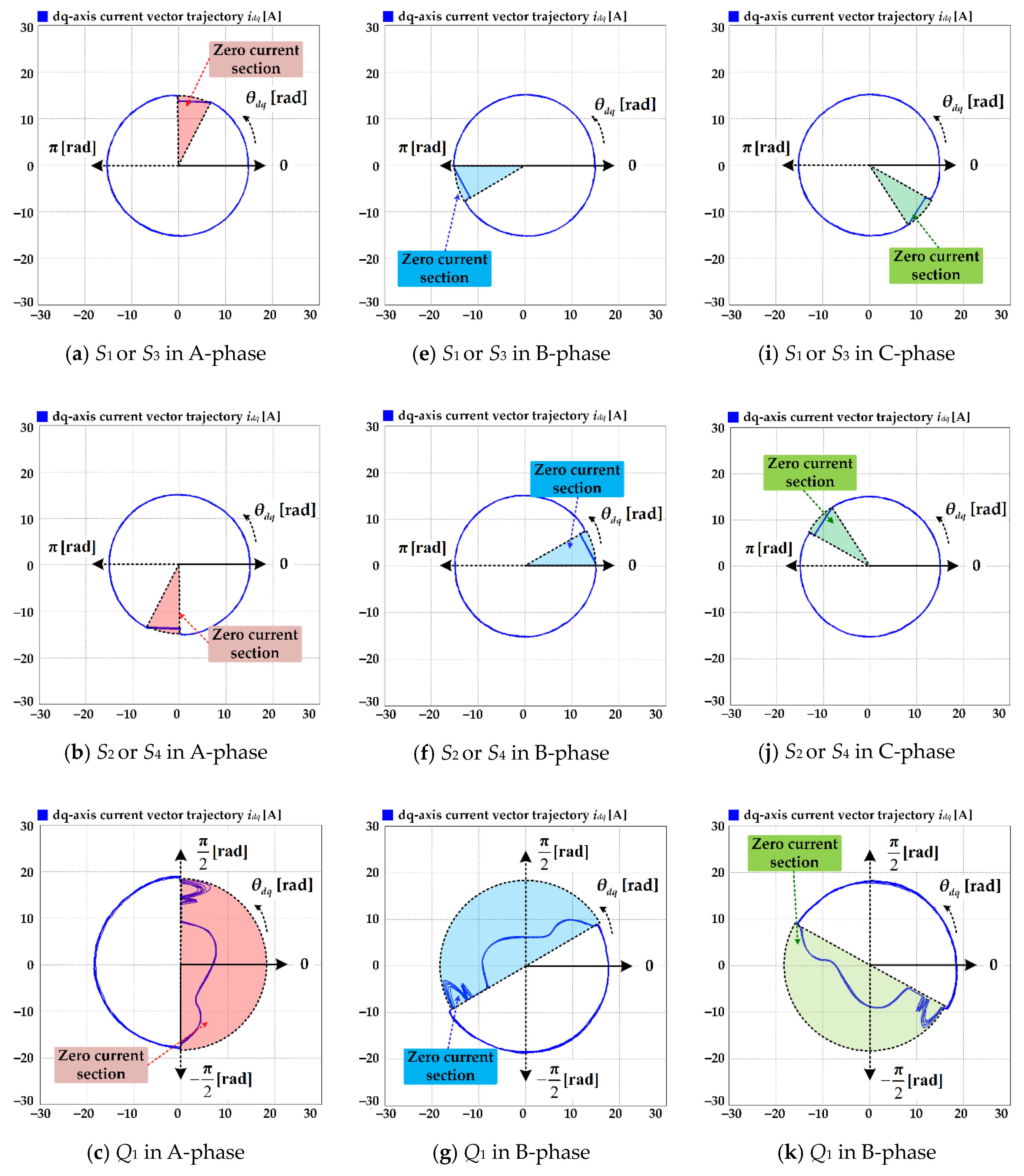
Figure 11 shows dq-axis Lissajous waveforms for all cases of open-switch fault. If one phase is a faulty leg, the zero current section appears in a certain angle range (θdq) of the Lissajous waveform. There are phase-angle differences between A/B, B/C, and C/A phase faulty conditions. The B-phase lags 120° behind the A-phase and the C-phase leads 120° in front of the A-phase. These angular characteristics help identify the faulty leg and type of fault that has occurred (IGBT or MOSFET). The zero-current section is expanded, when compared to that of the unity PF condition, which implies that more current flow has been blocked by the open-circuit, because of the PF control with d-axis current. Even though the multiple fault occurred in one or more phase, the circumstance is not different as far from earlier investigations. Because the multiple Si IGBT faults does not make any remarkable difference with normal condition when it comes to a unity PF, as presented in Figure 7b. But in the non-unity PF condition, if the open-faults of IGBT switches occurred in the one or more phases, the dq-current trajectory follows as a combination of particular zero current sections according to fault occurrence location as described in Figure 11. When the open faults happen in S1 switch of A and B-phase, the current vector trajectory shows two zero current section of Figure 11a,e. Also, the multiple SiC MOSFET faults detected by zero current sections in the related angle boundary for each phase as presented in Figure 11.
Instead of controlling the HANPC rectifier with a continuously non-unity PF, Figure 12 presents an intermittent d-axis current-injection method in the HANPC rectifier. In this procedure, the grid angle, which is derived by the PLL, is used to count the number of cycles. A count variable (x) increases when every grid period starts with a new period as a fundamental period. When the variable (x) reaches a certain number (k), the dq-axis reference change and phase current angle vary slightly. By counting and checking these variations, it is possible to apply the d-axis current in every kth period of the fundamental period. The variation of the dq-axis current reference also causes a change in the dq-axis current angle (θdq). However, if an open-switch fault occurs and reactive power flow is induced, the zero current comes out on the faulty phase current and dq-axis currents.
The zero-current section can be detected easily using a derivative value of the dq-axis current angle (dq/dt). The control variable k determines the timing of that current references change and the fault-detection process starts. As mentioned in Figure 9, the reactive current injection is necessary for a change in output waveforms of dq-axis currents. When we choose small k value like 2 or 3, the current references are harshly fluctuating and the output current characteristics get bad. On the other hand, if the k value is selected as a large value like 10 or bigger, that means the fault-detection procedure is executed very rarely, and this finally slows down detection time. So, the k value should be selected with careful consideration.
Figure 13 depicts the proposed fault-detection method, which is based on the phase current distortion in the HANPC rectifier. First, the counting process is executed in accordance with the synchronous grid phase angle (θgrid). The counting value (x) increases until it reaches a maximum value (k). When the fundamental period becomes equal to the kth period, the reactive current reference is applied during one cycle and the counting is reset to 1. Thereby, the reactive current is applied to each kth period during one cycle. In each kth period, the phase current is induced to be out of phase and the zero current section is detected if the open-switch fault occurs. The next step is to calculate and check the dq-current angle. The dq-current angle and its differential value are calculated from the dq-axis current, and the faulty phase current is detected when the differential value is zero. After the zero current section is detected by the dq-axis current, checking is performed to determine whether the zero current has occurred in the kth period or not. If the zero-current section exists in the non-kth period, the faulty location is diagnosed as a MOSFET switch. The faulty location is determined by the current angle value as categorized. Otherwise, if the zero current occurs in the kth period, because of the reactive power injection, the candidates for the faulty location are IGBTs and the designated numbers are 1–4. Using the current angle value when the zero current is detected, the candidates are distinguished as S1/S3 or S2/S4 switches. Finally, a suitable switching state (P or N) is employed, and an accurate faulty switch is diagnosed, according to the positive or negative current flow.

4. Simulation Results

Figure 14 shows the simulated waveforms for the proposed open-fault detection method for a HANPC rectifier. The open-fault scenario is assumed to be on a single transistor of the A-phase. In the simulation, the IGBT fault has already occurred and, in order to detect the open fault, the non-unity PF control is conducted every 6th fundamental period (k = 5).
As shown in Figure 14a,b, the S1 and S3 IGBT faults produce a phase current that is zero when the dq-current angle range is from 60° to 90°. The zero current appears on the dq-current angle waveform as well, because the current angle stays at the same value, without increasing. The S1 and S3 IGBT faults generate similar zero current sections, and it is necessary to distinguish which transistor is faulty, using the P switching state. The zero current is maintained even if the P switching state is applied under the S1 switch fault, as shown in Figure 14a, and the fault detection signal is set to 1. In addition, the S3 switch fault can generate a positive current with delicate P switching state injection, as shown in Figure 14b, and the fault is detected as number 3.
In Figure 14c,d, it is observed that the dq-current angle stops rising during an open fault when the dq-current angle range is from −120° to −90°. To distinguish the S4 switch fault from the S2 fault, the N switching state is applied during the zero-current section. The phase current value is zero despite the instant N switching state because the IGBT S4 is opened (Figure 14c). Under the neutral-point IGBT S2 fault case, negative current generation is feasible and the fault is diagnosed as 2, as in Figure 14d.
Two cases of MOSFET faults are possible in the A-phase, and the failure caused by the MOSFET switch leads to continuous current distortion. The upper MOSFET fault occludes the positive current flow; in other words, the sinusoidal current waveform is not generated. In the case of Q1 transistor fault, the derivative of the angle value is zero in the angle range from −90° to 90° (−90° ≤ θdq ≤ 90°); thus, the fault is detected as 5 in Figure 14e. The lower MOSFET fault stops the A-phase, to facilitate the O+ state, and distorts the phase current in the negative half period. The fault is detected as 6, because the dq-current angle does not increase when the dq-current angle is smaller than −90° or greater than 90° (θdq ≤ −90° or 90° ≤ θdq).

5. Experimental Results

The proposed open-fault detection algorithm was implemented in an experimental setup, which is described in Figure 15. The constituents of the 3-P HANPC rectifier system were the power stage, control stage, and other equipment such as oscilloscope, control PC, and low-voltage power supply. The power stage was built with Si IGBTs (SK75GBB066T, Semikron, Nuremberg, Germany), SiC MOSFETs (C2M0040120D, Cree, Raleigh, NC, USA), and gate drivers to operate each switching device. All the switches were mounted on a heat sink to dissipate the thermal radiation effectively and cool down the junction temperature during the AC to DC conversion. The control stage was composed of a digital signal processor (TMS320F28377S, TI, Dallas, TX, USA) and the PWM; an analog-to-digital conversion function was also employed. The digital processor computed the reference signal and produced the LF/HF PWM signal while sensing the analog signal using sensors [48]. The control variables used to control the HANPC rectifier were also displayed on oscilloscopes (HDO6104, Teledyne, Thousand Oaks, CA, USA) using a digital-to-analog conversion function. The low-voltage power supply functioned as a moderate power source for the gate drivers, sensors, and main control board. The control PC communicated with the control stage as well.
Figure 16 presents the experimental results for the proposed open-fault detection method. In the measured waveforms, the red, light blue, and yellow curves indicate the 3-P currents (A, B, and C phases, respectively), and the pink sawtooth lines and the blue horizontal lines indicate the dq-current angle and faulty switch location, respectively. The experimental specifications are the same as those presented in Table 2, and the control variable k is set as 6. For normal operation of the HANPC rectifier, the peak value of the 3-P phase current is controlled as 5 A, and there is a 120° phase-angle difference between each phase. In the normal unity-PF control situation, phase current distortion is not induced by IGBT failure unless a reactive current is applied. This phenomenon is presented in Figure 16a–d, which show the faulty cases of IGBT S1, S3, S4, and S2, respectively.
As shown in Figure 16a, the IGBT fault of the A-phase produces phase-current distortion, which means that the zero-current section is displayed by the reactive power injection. By checking the dq-current angle value, it is possible to detect the S1 open fault, but the switch S3 fault also generates confusable waveforms. The P switching state is applied manually, and the neutral-point switch S3 fault is distinguished from the S1 fault. When a positive current is induced, as in Figure 16b, the current flow implies that the S1 switch can normally operate whereas S3 cannot.
Figure 16c,d show the results of the experiment conducted under faulty conditions. Two cases have almost the same zero current section, although a d-axis current is applied. In order decide among the two candidates, the N switching state is applied in the middle of the zero-current section. A constant zero-current state exists, regardless of the N switching state, because switch S4 fails and the current path is disconnected to form an open circuit (Figure 16c). In addition, the neutral-point IGBT fault has a current path for the current, and a negative current flow is induced for a short time.
During the failure of MOSFET switches, the problem of injecting certain switching states is no matter with fault detection; however, the zero-current section is important for diagnosing the exact faulty location. The zero-current section is defined as the range in which the dq-axis current is distorted. Each MOSFET fault has its own range, as shown in Figure 11. As presented in Figure 16e,f, the MOSFET fault is detected immediately by checking the dq-current angle value. Therefore, the experimental results prove the effectiveness of the proposed fault-detection method.

6. Conclusions

This paper proposed an open-fault detection method for Si IGBTs and SiC MOSFETs used in a HANPC rectifier. The HANPC rectifier facilitated low power loss characteristics and cost-effective configuration by using Si IGBTs and SiC MOSFETs in a single power stage. To address the reliability issues associated with the HANPC rectifier, this paper addressed switch open-fault cases and analyzed the features of each switch fault. The proposed fault-detection algorithm used phase current and dq-axis current data to diagnose the faulty switch precisely. Moreover, the reactive current component was used to make a remarkable difference from the unity-PF condition. The Lissajous waveforms created by the dq-axis currents contained information on the faulty switch and helped the detect fault occurrence. After the fault was detected by the dq-current and its angular value, a special switching scheme was applied to distinguish similar faulty situations. Accurate fault detection was accomplished using the proposed fault-detection method, without requiring additional hardware or external circuit implementation. Simulations and experiments were conducted, which demonstrated the feasibility and effectiveness of the proposed fault-detection method.

Author Contributions

K.-B.L. provided guidance and supervision. S.P. conduced to review and edit the paper and revised the manuscript as well. S.-M.K. built a hardware set-up and administrated this project. S.-H.K. performed the simulation, experiment. All authors have equally contributed to the simulation analysis, experiment, and result discussions. All authors have read and agreed to the published version of the manuscript.

Funding

This work was supported by the Korea Institute of Energy Technology Evaluation and Planning (KETEP) and the Ministry of Trade, Industry & Energy (MOTIE) of the Republic of Korea. (No. 20182410105160, No. 20206910100160).

Acknowledgments

Authors thank our Power Electronics Laboratory colleagues of Electrical & Computer Engineering Department, Ajou University, South Korea.

Conflicts of Interest

The authors declare no conflict of interest.

References

  1. Lee, K.B.; Lee, J.S. Reliability Improvement Technology for Power Converters, 1st ed.; Springer: Singapore, 2017; ISBN 978-981-10-4991-0. [Google Scholar]
  2. Bak, Y.; Lee, K.-B. Development of PCS to utilize differential pressure energy in district heating systems with reduced DC-link voltage variation. J. Power Electron. 2020, 20, 1109–1118. [Google Scholar] [CrossRef]
  3. Lee, S.S.; Bak, Y.; Kim, S.-M.; Joseph, A.; Lee, K.-B. New family of boost switched-capacitor seven-level inverters (BSC7LI). IEEE Trans. Power Electron. 2019, 34, 10471–10479. [Google Scholar] [CrossRef]
  4. Blaabjerg, F.; Chen, J.; Kjaer, S.B. Power electronics as efficient interface in dispersed power generation systems. IEEE Trans. Power. Electron. 2004, 19, 1184–1194. [Google Scholar] [CrossRef]
  5. Lee, C.-H.; Lee, J. An Optimal Damping Control Algorithm of Direct Two-level Inverter for Miniaturization and Weight Reduction of Auxiliary Power Supply on Railway Vehicle. J. Electr. Eng. Technol. 2018, 13, 2335–2343. [Google Scholar] [CrossRef]
  6. Slaman, S.; Xin, A. Droop Control based Approach for Frequency and Voltage in Hybrid AC/DC Microgrid. J. Electr. Eng. Technol. 2020, 15. [Google Scholar] [CrossRef]
  7. Zhang, T.; Chen, X.; Qi, C.; Lang, Z. Leg-By-Leg-Based Finite-Control-Set Model Predictive Control for Two-Level Voltage-Source Inverters. J. Power Electron. 2019, 19, 1162–1170. [Google Scholar] [CrossRef]
  8. Bak, Y.; Jang, Y.; Lee, K.-B. Torque Predictive Control for Permanent Magnet Synchronous Motor Drives Using Indirect Matrix Converter. J. Power Electron. 2019, 19, 1536–1543. [Google Scholar] [CrossRef]
  9. Rodríguez, J.; Lai, J.-S.; Peng, F.Z. Multilevel inverters: A survey of topologies, controls, and applications. IEEE Trans. Ind. Electron. 2002, 49, 724–738. [Google Scholar] [CrossRef] [Green Version]
  10. Huo, Q.; Wang, P.; Cao, G.; Zhu, J.; Yin, J.; Guo, X.; Wei, T. Novel flexible HVDC transmission converter station topology with DC fault blocking capability. J. Power Electron. 2020, 20, 884–893. [Google Scholar] [CrossRef]
  11. Rodríguez, J.; Bernet, S.; Wu, B.; Pontt, J.O.; Kouro, S. Multilevel voltage-source-converter topologies for industrial medium-voltage drives. IEEE Trans. Ind. Electron. 2007, 54, 2930–2945. [Google Scholar] [CrossRef]
  12. Rodriguez, J.; Bernet, S.; Steimer, P.K.; Lizama, I.E. A survey on neutral-point-clamped inverters. IEEE Trans. Ind. Electron. 2010, 57, 2219–2230. [Google Scholar] [CrossRef]
  13. Schweizer, M.; Friedli, T.; Kolar, J.W. Comparative evaluation of advanced three-phase three-level inverter/Converter topologies against two-level systems. IEEE Trans. Ind. Electron. 2013, 60, 5515–5527. [Google Scholar] [CrossRef]
  14. Rodríguez, J.; Dixon, J.; Espinoza, J.; Pontt, J.; Lezana, P. PWM Regenerative rectifiers: State of the art. IEEE Trans. Ind. Electron. 2005, 52, 5–22. [Google Scholar] [CrossRef]
  15. Nabae, A.; Takahashi, I.; Akagi, H. A new neutral-point-clamped PWM inverter. IEEE Trans. Ind. Appl. 1981, IA-17, 518–523. [Google Scholar] [CrossRef]
  16. Brückner, T.; Bernet, S.; Güldner, H. The active NPC converter and its loss-balancing control. IEEE Trans. Ind. Electron. 2005, 52, 855–868. [Google Scholar] [CrossRef]
  17. Millán, J.; Godignon, P.; Perpiñà, X.; Pérez-Tomás, A.; Rebollo, J. A survey of wide bandgap power semiconductor devices. IEEE Trans. Power Electron. 2014, 29, 2155–2163. [Google Scholar] [CrossRef]
  18. She, X.; Huang, A.Q.; Lucía, Ó.; Ozpineci, B. Review of Silicon Carbide Power Devices and Their Applications. IEEE Trans. Ind. Electron. 2017, 64, 8193–8205. [Google Scholar] [CrossRef]
  19. Wang, J.; Jiang, X. Review and analysis of SiC MOSFETs’ ruggedness and reliability. IET Power Electron. 2020, 13, 445–455. [Google Scholar] [CrossRef]
  20. Guan, Q.-X.; Li, C.; Zhang, Y.; Wang, S.; Xu, D.-D.; Li, W.; Ma, H. An extremely high efficient three-level active neutral-point-clamped converter comprising SiC and Si hybrid power stages. IEEE Trans. Power Electron. 2018, 33, 8341–8352. [Google Scholar] [CrossRef]
  21. Yang, S.; Bryant, A.; Mawby, P.; Xiang, D.; Ran, L.; Tavner, P. An industry-based survey of reliability in power electronic converters. IEEE Trans. Ind. Appl. 2011, 47, 1441–1451. [Google Scholar] [CrossRef]
  22. Choi, U.-M.; Blaabjerg, F.; Lee, K.-B. Study and handling methods of power IGBT module failures in power electronic converter systems. IEEE Trans. Power Electron. 2015, 30, 2517–2533. [Google Scholar] [CrossRef]
  23. Yang, S.; Xiang, D.; Bryant, A.; Mawby, P.; Ran, L.; Tavner, P. Condition monitoring for device reliability in power electronic converters: A review. IEEE Trans. Power Electron. 2010, 25, 2734–2752. [Google Scholar] [CrossRef]
  24. Liu, G.; Li, K.; Wang, Y.; Luo, H.; Luo, H. Recent advances and trend of HEV/EV-oriented power semiconductors—An overview. IET Power Electron. 2020, 13, 394–404. [Google Scholar] [CrossRef]
  25. Yang, H.; Zhou, Y.; Zhao, J. Current covariance analysis-based open-circuit fault diagnosis for voltage-source-inverter-fed vector-controlled induction motor drives. J. Power Electron. 2020, 20, 492–500. [Google Scholar] [CrossRef]
  26. Lu, B.; Sharma, S.K. A literature review of IGBT fault diagnostic and protection methods for power inverters. IEEE. Trans. Ind. Appl. 2009, 45, 1770–1777. [Google Scholar] [CrossRef]
  27. Mohan, M.; Vittal, K.P. DC Fault Protection in Multi-terminal VSC-Based HVDC Transmission Systems with Current Limiting Reactors. J. Electr. Eng. Technol. 2019, 14, 1–12. [Google Scholar] [CrossRef]
  28. Shin, H.-U.; Lee, K.-B. Fault Diagnosis Method for Switched Reluctance Machine Drive Systems Using a Switching Signal. J. Electr. Eng. Technol. 2019, 14, 663–676. [Google Scholar] [CrossRef]
  29. Lin, Y.; Ge, H.; Chen, S.; Pecht, M. Two-level fault diagnosis RBF networks for auto-transformer rectifier units using multi-source features. J. Power Electron. 2020, 20, 754–763. [Google Scholar] [CrossRef]
  30. Yin, H.; Chen, Y.; Chen, Z. Observer-based adaptive threshold diagnosis method for open-switch faults of voltage source inverters. J. Power Electron. 2020, 20. [Google Scholar] [CrossRef]
  31. Kim, Y.; Park, T.; Kim, S.; Kwak, N.; Kweon, D. Artificial Intelligent Fault Diagnostic Method for Power Transformers using a New Classification System of Faults. J. Electr. Eng. Technol. 2019, 14, 825–831. [Google Scholar] [CrossRef]
  32. Im, W.-S.; Kim, J.-M.; Lee, D.-C.; Lee, K.-B. Diagnosis and fault-tolerant control of three-phase AC–DC PWM Converter SYSTEMS. IEEE Trans. Ind. Appl. 2013, 49, 1539–1547. [Google Scholar] [CrossRef]
  33. Cardoso, A.M.; Saraiva, E.S. Computer-aided detection of airgap eccentricity in operating three-phase induction motors by Park’s vector approach. IEEE Trans. Ind. Appl. 1993, 29, 897–901. [Google Scholar] [CrossRef]
  34. Jo, S.-R.; Kim, S.-M.; Cho, S.; Lee, K.-B. Development of a hardware simulator for reliable design of modular multilevel converters based on junction-temperature of IGBT modules. Electronics 2019, 8, 1127. [Google Scholar] [CrossRef] [Green Version]
  35. Choi, U.-M.; Blaabjerg, F.; Jørgensen, S. Power cycling test methods for reliability assessment of power device modules in respect to temperature stress. IEEE Power Electron. 2018, 33, 2531–2551. [Google Scholar] [CrossRef] [Green Version]
  36. Alavi, M.; Wang, D.; Luo, M. Short-circuit fault diagnosis for three-phase inverters based on voltage-space patterns. IEEE Trans. Ind. Electron. 2014, 61, 5558–5569. [Google Scholar] [CrossRef]
  37. Gao, Z.; Cecati, C.; Ding, S.X. A Survey of fault diagnosis and fault-tolerant techniques—Part I: Fault diagnosis with model-based and signal-based approaches. IEEE Trans. Ind. Electron. 2015, 62, 3757–3767. [Google Scholar] [CrossRef] [Green Version]
  38. Ku, H.-K.; Jung, J.-H.; Park, J.-W.; Kim, J.-M. Fault-tolerant control strategy for open-circuit fault of two-parallel-connected three-phase AC–DC two-level PWM converter. J. Power Electron. 2020, 20, 731–742. [Google Scholar] [CrossRef]
  39. Lee, E.; Lee, K.-B. Fault-tolerant strategy to control a reverse matrix converter for open-switch faults in the rectifier stage. J. Power Electron. 2016, 16, 57–65. [Google Scholar] [CrossRef] [Green Version]
  40. Khomfoi, S.; Tolbert, L.M. Fault diagnostic system for a multilevel inverter using a neural network. IEEE Trans. Power Electron. 2007, 22, 1062–1069. [Google Scholar] [CrossRef]
  41. Qiao, H.; Wang, T.; Wang, P.; Zhang, L.; Xu, M. An adaptive weighted multiscale convolutional neural network for rotating machinery fault diagnosis under variable operating conditions. IEEE Access 2019, 7, 118954–118964. [Google Scholar] [CrossRef]
  42. Caseiro, L.M.A.; Mendes, A.M.S. Real-time IGBT open-circuit fault diagnosis in three-level neutral-point-clamped voltage-source rectifiers based on instant voltage error. IEEE Trans. Ind. Electron. 2015, 62, 1669–1678. [Google Scholar] [CrossRef]
  43. Kwon, B.H.; Kim, S.-H.; Kim, S.-M.; Lee, K.-B. Fault diagnosis of open-switch failure in a grid-connected three-level Si/SiC hybrid ANPC inverter. Electronics 2020, 9, 399. [Google Scholar] [CrossRef] [Green Version]
  44. Choi, U.-M.; Jeong, H.-G.; Lee, K.-B.; Blaabjerg, F. Method for detecting an open-switch fault in a grid-connected NPC inverter system. IEEE Trans. Power Electron. 2012, 27, 2726–2739. [Google Scholar] [CrossRef]
  45. Kim, T.-J.; Lee, W.-C.; Hyun, D.-S. Detection method for open-circuit fault in neutral-point-clamped inverter systems. IEEE Trans. Ind. Electron. 2009, 56, 2754–2763. [Google Scholar] [CrossRef]
  46. Afef, B.-B.A.; Hafedh, B.A.; Frédéric, R.; Jean-Marc, B.; Franck, M.; Ilhem, S.-B. Versatile three-level FC-npc converter with high fault-tolerance capabilities: Switch fault detection and isolation and safe postfault operation. IEEE Trans. Ind. Electron. 2019, 64, 6453–6464. [Google Scholar] [CrossRef]
  47. Qun-Tao, A.; Li-Zhi, S.; Ke, Z.; Li, S. Switching function model-based fast-diagnostic method of open-switch faults in inverters without sensors. IEEE Trans. Power Electron. 2011, 26, 119–126. [Google Scholar] [CrossRef]
  48. Jeon, S.-S.; Lee, Y.J.; Bak, Y.; Lee, K.-B. Hardware-simulator development and implementation for hydraulic turbine generation systems in a district heating system. Electronics 2020, 9, 368. [Google Scholar] [CrossRef] [Green Version]
  49. Seo, D.-W.; Bak, Y.; Lee, K.-B. An improved rotating restart method for a sensorless permanent magnet synchronous motor drive system using repetitive zero voltage vectors. IEEE Trans. Ind. Electron. 2020, 67, 3496–3504. [Google Scholar] [CrossRef]
  50. Lee, E.-J.; Kim, S.-M.; Lee, K.-B. Modified phase-shifted PWM scheme for reliability improvement in cascaded H-bridge multilevel inverters. IEEE Access 2020, 8, 78130–78139. [Google Scholar] [CrossRef]
  51. Kim, S.-M.; Jeong, M.-G.; Kim, J.; Lee, K.-B. Hybrid Modulation Scheme for Switching Loss Reduction in a Modular Multilevel High-voltage Direct Current Converter. IEEE Trans. Power Electron. 2019, 34, 3178–3191. [Google Scholar] [CrossRef]
  52. Kwon, B.H.; Kim, S.-H.; Bea, K.-C.; Lee, K.-B. Performance analysis on a bidirectional operation of a three-level hybrid ANPC inverter. Trans. Korean Inst. Electr. Eng. 2019, 10, 1204–1213. [Google Scholar] [CrossRef]
  53. Yoon, H.; Yoon, D.; Choi, D.; Cho, Y. Three-phase current balancing strategy with distributed static series compensators. J. Power Electron. 2019, 19, 803–814. [Google Scholar] [CrossRef]
  54. Choi, H.; Song, S.; Jeong, S.; Choi, J.; Choy, I. Design of SRF-PLL system with consideration of low-pass filter for high dynamic performance during voltage disturbance. In Proceedings of the IEEE 6th International Power Electronics and Motion Control Conference (IPEMC), Wuhan, China, 17–20 May 2009. [Google Scholar] [CrossRef]
  55. Xu, Y.; Li, H.; Ren, J.; Zhang, Y. Three-vector-based model predictive current control with disturbance feedforward compensation. J. Power Electron. 2020, 20, 687–697. [Google Scholar] [CrossRef]
  56. Feng, X.; Tao, Y.; Cui, X.; Shao, K.; Wang, Y. Sliding mode and predictive current control strategy of the three-phase Vienna rectifier. J. Power Electron. 2020, 20, 743–753. [Google Scholar] [CrossRef]
  57. Kazmierkowski, M.P.; Malesani, L. Current control techniques for three-phase voltage-source PWM converters: A survey. IEEE Trans. Ind. Electron. 1998, 45, 691–703. [Google Scholar] [CrossRef]
  58. Lee, J.-S.; Lee, K.-B.; Blaabjerg, F. Open-switch fault detection method of a back-to-back converter using NPC topology for wind turbine systems. IEEE Trans. Ind. Appl. 2015, 51, 325–335. [Google Scholar] [CrossRef]
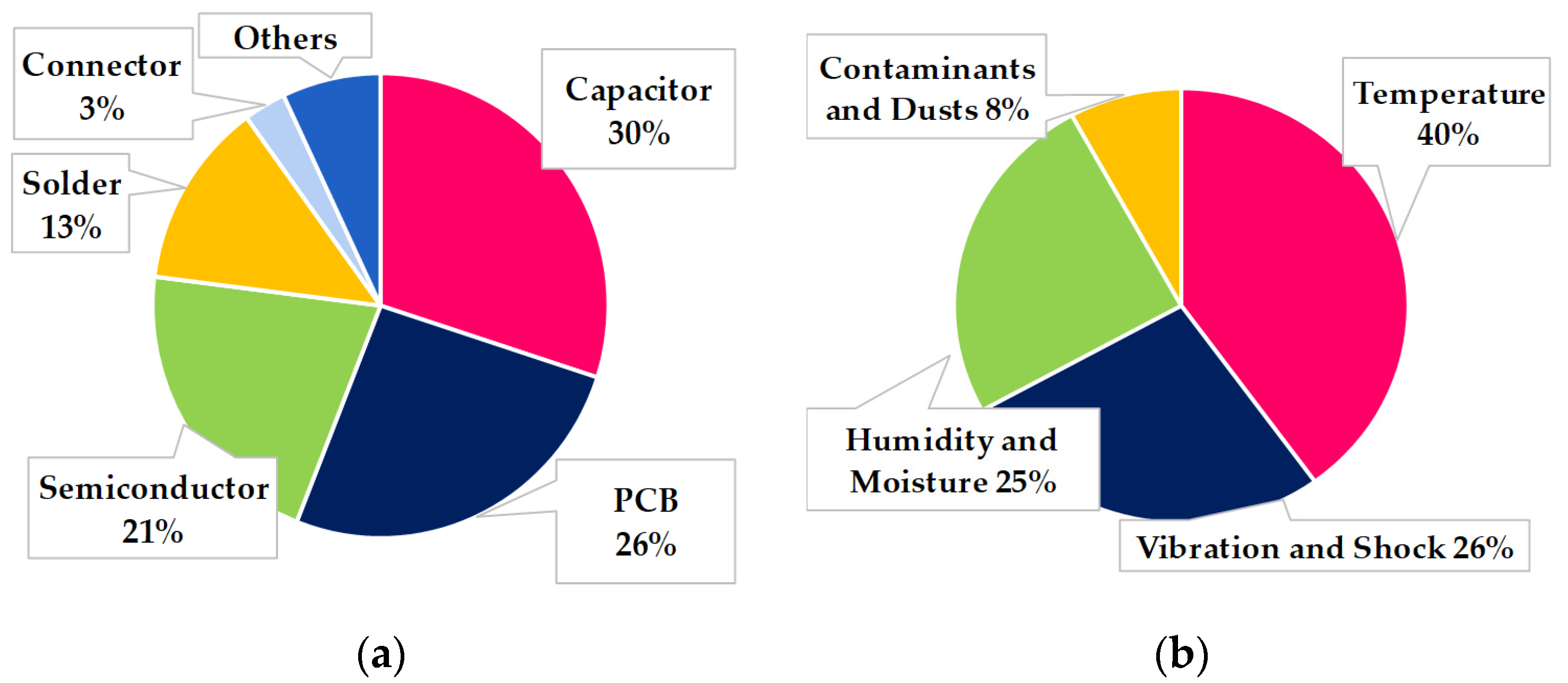
Figure 1. Failure distribution in power electronics systems: (a) Fault components in power converters; (b) Failure influence factors.
Electronics 09 01437 g001
Figure 2. Types of 3-L VSCs: (a) DNPC-type; (b) ANPC-type; (c) HANPC-type.
Electronics 09 01437 g002
Figure 3. Operation principle of the HANPC inverter: (a) Reference voltages for each phase and common offset voltage; (b) Normalized reference voltage and triangular carrier wave; (c) Gate signals for Si IGBTs and SiC MOSFETs; (d) Three-level output pole voltage.
Electronics 09 01437 g003
Figure 4. Switching states and current path of the HANPC rectifier.
Electronics 09 01437 g004
Figure 5. Phase current and pole voltage under each IGBT faulty condition in the HANPC rectifier.
Electronics 09 01437 g005
Figure 6. Phase current and pole voltage under each MOSFET faulty condition in the HANPC rectifier.
Electronics 09 01437 g006
Figure 7. Current vector trajectory in stationary reference frame.
Electronics 09 01437 g007
Figure 8. Control diagram for three-phase HANPC rectifier.
Electronics 09 01437 g008
Figure 9. Faulty phase current, dq-axis current and current vector angle waveforms for zero current section under A-phase single switch fault in the HANPC rectifier (PF = 3 / 2 ).
Electronics 09 01437 g009aElectronics 09 01437 g009b
Figure 10. Process to identify a faulty location in two Si IGBT candidates switches by using P or N switching state.
Electronics 09 01437 g010
Figure 11. Current vector trajectories according to each faulty case (PF = 3 / 2 ).
Electronics 09 01437 g011aElectronics 09 01437 g011b
Figure 12. Voltage and current waveforms when intermittent d-axis current injected for IGBT open-switch fault in the HANPC rectifier (k = 2).
Electronics 09 01437 g012
Figure 13. Flowchart of the proposed detection method for open-switch fault in the HANPC rectifier.
Electronics 09 01437 g013
Figure 14. Simulation waveforms of phase current, current angle, and fault detection signals for each switch failure in the HANPC rectifier.
Electronics 09 01437 g014
Figure 15. Experimental setup of three-phase HANPC rectifier system.
Electronics 09 01437 g015
Figure 16. Experimental waveforms of phase current, current angle, and fault detection signals for each switch failure in the HANPC rectifier.
Electronics 09 01437 g016
Table 1. Switching states and output pole voltage in accordance with on-off state of each switch in the HANPC topology (1: on, 0: off).
Switching StateOutput Pole Voltage VxnIGBTsMOSFETs
S1S2S3S4Q1Q2
Positive (P)+VDC/2101010
Zero (O+)0101001
Zero (O−)0010110
Negative (N)VDC/2010101
Table 2. Parameters of HANPC rectifier.
ParametersValueUnit
Voltage of DC-link (VDC)600V
Voltage of grid source (line-to-line)380Vrms
Capacitance of DC-link (Cupper, Clow)4700μF
Inductance of grid filter (L)2mH
Switching frequency of SiC MOSFET20,000Hz
Frequency of grid voltage (switching frequency of Si IGBT)60Hz