Abstract
As one of the fundamental elements of the fingerprints of integrated circuit chips, static random-access memory based physical unclonable function (SRAM PUF) has been regarded as an attractive option for hardware security circuits. Commercial SRAM chips could be used as PUF chips for low cost systems. However, the mismatches existing in most commercial SRAM chips are quite small, which could result in poor stability of SRAM PUF. To address this issue, this paper proposes a novel SRAM PUF stability improvement method using total ionization dose (TID) effect for commercial SRAM chips. The principles of this new method are presented in detail and verified by simulations. Thereafter, the TID experiments are carried out on one kind of commercial SRAM chips and validate that this novel method could reduce the intra-chip hamming distance (𝐻𝐷_𝑖𝑛𝑡𝑟𝑎) by two orders of magnitude within the ionizing dose range of 40–100 Krad (SiO2), which is a significant stability improvement. Furthermore, considering the trade-offs of other performance factors, 40 Krad (SiO2) has been regarded as the recommended ionizing dose, which not only makes the stability and uniformity of SRAM PUF attain almost ideal values but also keeps the radiation-induced damage within a limited level.
1. Backgrounds
In general, a physical unclonable function (PUF) is an entity that uses random manufacturing process variations to generate device-specific outputs which can be used to extract inherent device fingerprints or unique cryptographic keys [1,2]. PUFs have recently been regarded as a more innovative security technology over traditional methods for superior security performance, lower cost and resilience to reverse engineering [3,4]. In the past few years, quite a variety of PUF approaches have been developed, which can be categorized as non-silicon PUFs and electronic PUFs [1].
One typical representative of non-silicon PUFs is Quantum Optical PUF (Q-OPUF) [1,5], which utilizes nanometer-scale fabrication defects in sheets of 2D materials to generate random spatial variations in their bandgap. The variations of nanometer-scale help to resist any physical cloning. However, Q-OPUF needs peculiar materials and specialized equipment, which add complexity to the PUF response extraction process [1].
Ring Oscillator PUF (RO PUF) [6], Arbiter PUF [7] and static random-access memory based physical unclonable function (SRAM PUF) [8] are commonly recognized as classic electronic PUF designs [9]. RO PUF compares the oscillation frequencies of the Ros to generate chip-specific codes. RO PUF is easy to implement on a field-programmable gate array (FPGA) but it is vulnerable to attack utilizing the frequency distribution characteristics of the RO arrays [6]. Arbiter PUF derives response by comparing two identical delay paths. As one kind of strong PUF, Arbiter PUF possesses sufficient change-response pairs [1] but its circuit structure and layout implementation must satisfy very stringent symmetry regulations [10].
As for SRAM PUF, due to unpredictable technology variations in the production process, every transistor in static random-access memory (SRAM) cells has slightly random electric properties [11]. This randomness manifests as the power-on values of SRAM memory [12]. Compared to other existing PUF technologies, SRAM PUF possesses the following advantages.
Unlike non-silicon PUFs, SRAM power-on values can be directly read as binary codes, so there is no need for complex PUF response extraction operations [1]. Compared to RO PUF and Arbiter PUF, SRAM PUF can reuse on-chip SRAM memory or commercial off-the-shelf SRAM chips [13]. This dramatically decreases the product development costs and eases integration difficulties.
Due to the above factors, SRAM PUF increasingly attracts researchers’ exploration around the world, it is also the most popular commercial PUF component which is valued by advanced hardware security solution suppliers such as NXP [14], intrinsic ID [15] and Microsemi [16] and so on.
2. Introduction
In recent years, great progress has been made in the academic research and commercial applications of SRAM PUF [5,6]. Whereas, SRAM PUF is still faced with several critical challenges, for example, voltage fluctuation, temperature variation and environmental noise may make SRAM PUF unstable between readings [17]; and the number of ‘0’s in the SRAM power-on values can become much larger than that of ‘1’s or vice versa due to asymmetric layout or unpredictable large systematic process variation [18].
Various methods have been adopted to overcome the above issues, especially to improve stability. As SRAM PUF was first proposed in 2007, Guajardo and Kumar et al. [8] utilized error correction codes (ECC) to correct the errors in the raw SRAM power-on values. Unfortunately, ECC blocks such as Bose–Chaudhuri–Hocquenghem (BCH) generally have high overheads [19] and the overheads scale up quickly with the error correction capability. Alternately, researchers have developed various techniques to increase the stability of raw SRAM power-on sequence and reduce the overheads of ECC. These techniques commonly employ one or more of the following ways.
- Modifying Cell Structure
On the basis of the standard SRAM cell circuit consisting of six transistors, several novel cell structures have been proposed to enlarge the mismatches in cells and improve SRAM PUF stability. Jang and Ghosh [20] harnessed the embedded PMOS latch and Magnetic Tunnel Junction (MTJ) to enhance mismatches in SRAM cells according to their initialized values of the first power-on cycle, thereafter, the cells will be steadily initialized to the same state as the first cycle. Beyond that, Okumura and Yoshimoto et al. [21] modified write drivers and power switches in SRAM cells to achieve low-power and high-reliability fingerprint generation. Zhang and Wang et al. [22] proposed one kind of SRAM PUF cell with isolated NMOS to improve the stability of the circuit. In general, considerable stability enhancement can be obtained by novel cell circuits but the long design cycle and high cost for tape-out and verification may become the main bottlenecks for general commercial applications.
- Aging Injection
Negative-bias-temperature-instability (NBTI) is one of the aging mechanisms [23]. NBTI occurs when a PMOS device is subjected to negative bias (i.e., ) on gate under high operating temperatures and this effect increases the device threshold voltage. Inspired by this phenomenon, Garg and Kim [24] proposed one stability solution by flipping the data in the SRAM array and injecting NBTI. However, the aging injection procedure must continue at least 6 h to achieve a remarkable stability improvement in this work.
- Masking and Preselection
In preselection, unstable cells are masked and excluded from the PUF response. Temporal majority voting (TMV) [25] is one commonly used primitive in preselection, which improves stability by powering on SRAM for many times and taking the majority of power-on values as the final output. Other mature methods are also compounded with TMV to further enhance stability, for example, Mathew et al. [26] provided a combination of TMV, aging injection and ECC circuits to reach a high stability level. However, these hybrid approaches bring out heavy hardware overheads, the adoption of TMV also introduces a long preselection period [13,27].
Liu and Zhou et al. [13] offered one more efficient preselection strategy making use of data remanence effect. This approach requires only two remanence tests—writing ‘1’ (or ‘0’) to the entire array and momentarily shutting down the power until a few cells flip and the easily flipped cells are the most robust ones. Almost 100% stable bits can be generated by the scheme but many stable cells are identified as unstable ones (e.g., over-selection) so that only a small portion of memory cells can be utilized. To make matters worse, the selected cells randomly straggle across the whole chip, which encumbers reusing SRAM chip to store data in source-constraint internet of things (IOT) devices [12].
While lots of previous works have put forward different kinds of solutions to improve SRAM PUF stability, we still seek a novel method exposing power-on SRAM chips to irradiation source for several minutes, which can enlarge mismatches of SRAM cells without necessity to modify circuit structure. The proposed method is easier and lower-cost than modifying cell structure and more efficient than applying aging injection. Compared to the preselection strategies, our solution will not waste memory capacity.
We elaborate on this novel scheme in the next sections. The physical mechanisms and basic principles of this method are presented in Section 3. Simulations are carried out to evaluate its correctness and effectiveness in Section 4. Subsequently, TID experiments are applied to verify the feasibility of the novel method on commercial SRAM chips in Section 5. Finally, conclusions are drawn in Section 6.
3. Principles of Proposed Methodology
The stability improvement of SRAM start-up values is obtained by applying ionization radiation on SRAM cells to enlarge their mismatches after they are powered on. In this section, the physical mechanisms and basic principles behind this novel method will be discussed based on irradiation-induced threshold voltage shift.
3.1. TID Effect on Transistors’ Threshold Voltages
Total ionizing dose effect (TID) refers to the cumulative effect on the semiconductor devices caused by ionizing radiation over the exposition time [28,29]. Many research works have revealed that TID effect causes slow change of the device’s electrical properties, such as the transistor’s threshold voltage, off-state current, subthreshold swing and carrier mobility [30]. We test the impact of TID effect on the threshold voltages of both P-channel Metal Oxide Semiconductor (PMOS) and N-channel Metal Oxide Semiconductor (NMOS) transistors fabricated in 180 nm Bulk CMOS technology and experimental results are shown in Figure 1. The figure illustrates that TID induced threshold shift is dependent on device type (NMOS or PMOS) and voltage bias (on or off-state). The effect of radiation makes threshold voltage of NMOS lower (easier to switch on) for both the on/off states and the reduction is larger at on-state. Whereas, the effect of radiation makes the absolute value of threshold voltage of PMOS higher (more difficult to switch on) and the increment is larger at off-state.
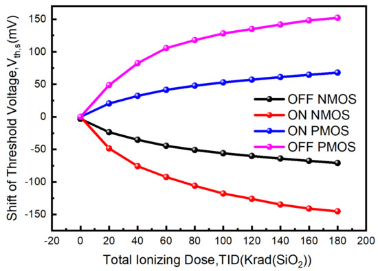
Figure 1.
Threshold voltage shift of transistors as a function of ionizing dose and voltage bias.
3.2. Physical Mechanisms of Stability Improvement Benefiting from TID Effect
Figure 2 shows the schematic of a 6T SRAM cell formed of two cross-coupled inverters and two access transistors and its power-on characteristic is mainly determined by the mismatch of two cross-coupled inverters, especially the threshold voltages of transistors [3]. According to the measurements in literatures [3,24,31], if the mismatch of two PMOS transistors’ threshold voltages ( is sufficiently large, it should be regarded as a strong cell. In this case, the bigger is, the more stable power-on data of the cell will be. Conversely, if is very small (, it should be taken as a weak cell. In such case, the power-on process is determined mainly by the mismatch of two NMOS transistors’ threshold voltages (. And the bigger is, the more stable power-on characteristic will be.
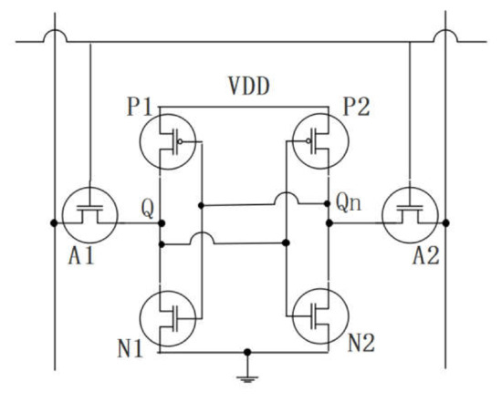
Figure 2.
Schematic of 6T static random-access memory (SRAM) cell.
When we discuss TID’s effect on the stability of SRAM power-on characteristic, SRAM is powered on and exposed to irradiation and it is necessary to distinguish between strong cells and weak ones.
For a strong cell shown in Figure 3, we primarily concern about the two PMOS transistors (P1 and P2) and assume that before irradiation, which means P2 is OFF-state while P1 is ON-state in the irradiation experiment. TID effect makes increase more than according to Figure 1. So of P1 and P2 will shift as follows.
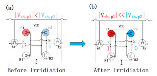
Figure 3.
(a) Strong cell before irradiation and (b) Strong cell after irradiation. If a strong cell outputs stable logic ‘1’ before irradiation, it will output more stable logic ‘1’ after irradiation.
It is obvious that from Equation (4), that is to say the mismatch of the two PMOS transistors will get bigger after irradiation and power-on data of the corresponding SRAM cell will become more stable.
When it comes to a weak cell shown in Figure 4, we mainly focus on the two NMOS transistors (N1 and N2) and assume that . It can be seen from Figure 1 that TID effect makes of the power-on NMOS transistor (N1) decrease more than that of the power-off one (N2). So of N1 and N2 will shift as follows.
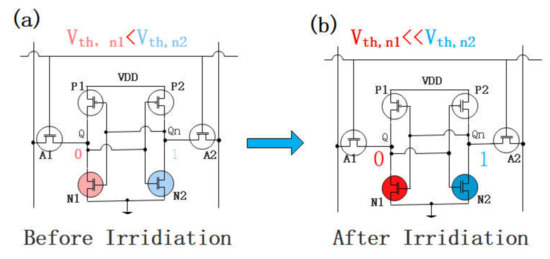
Figure 4.
(a) Weak cell before irradiation and (b) weak cell after irradiation. If a weak cell outputs unstable logic ‘0’ before irradiation, it will output stable logic ‘0’ after irradiation.
It is obvious that from Equation (8) and that is to say the mismatch of the two NMOS transistors will get bigger after irradiation and power-on data of the corresponding cell will become more stable too.
To sum up the above arguments, as long as one SRAM cell is powered on during irradiation, TID effect will always enhance the mismatch of transistors, which dominates its power-on state. As a result, the stability of its power-on state will be strengthened.
4. Simulations
In this section, transient noise simulations are carried out to verify the correctness of the theoretical analysis discussed in Section 3 and evaluate the efficiency of the proposed method.
Transient noise analysis is one upgrade of transient analysis for circuit simulation. It can show the effect of noise on the signal magnitude and it is also useful to see how noise effects the timing of the signal [32]. The power-on process of one practical SRAM cell is a noisy transient event which just sustains for several nanoseconds. Therefore, transient noise analysis is actually suitable to simulate the power-on process.
On the bias of transient noise analysis, if we can control the mismatch of the device parameters invoked in the circuit netlist, it will be convenient to assess how the mismatch affects the power-on stability of SRAM cells under certain noise level. That is to say the noise should be set appropriately at the initial transient noise simulation and will not change at subsequent simulations and then transient noise simulations will be repeated with the mismatch of device parameters changed.
We follow the instruction of the above proposed idea to simulate the effects of of transistors on the power-on stability of SRAM cells, which is deduced by TID effect and the applied device spice models are selected from BSIM3 180 nm models. The simulations are carried out according to these steps:
1. Run the initial transient noise analysis (add ‘.TRANNOISE METHOD = MC SAMPLES = 1000′ command in spice netlist ). Under this setting, 1000 power-on processes of one same cell will be simulated under the impact of random noise). Therefore, for the simulated cell, the probabilities of its power-on data being initialized to ‘0’ and ‘1’ are calculated as:
If , the power-on data is random and stability of the cell is weak. If , the power-on data tends to be stable as ‘0′, conversely, the power-on data tends to be stable as ‘1’.
2. The values of and under certain total ionizing dose can be extracted from the test results shown in Figure 1. The definitions of of transistor spice models are changed to fit these values and then the same transient noise simulation as in step 1 will be repeated under several kinds of mismatch conditions resulted from TID effect. will be recorded to evaluate the stability of the SRAM cell under every mismatch condition.
For a strong cell, PMOS transistors dominate its power-on behavior as discussed in Section 3. Thus, for simplification, the will be added step-by-step and the will always be equal to zero in simulations. The simulation results are shown in Figure 5 and Figure 6, there are non-linear increasing relationships between total ionizing dose and for both figures. As deduced by TID increases, if is larger and larger than , the power-on data of the cell will be more and more stable as ‘0′ shown in Figure 5, otherwise the power-on data of the cell will be more and more stable as ‘1′ shown in Figure 6. It is also noteworthy for both Figures that the probability of ‘0′ or ‘1′ will become more than 0.9 when the dose accumulates to 40 Krad (SiO2) and the increases to approximately 50 mV.
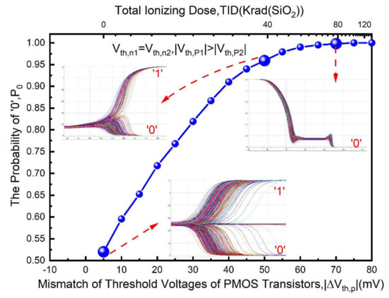
Figure 5.
Simulation results for a strong cell (), it tends to be initialized to 0 as dose increases.
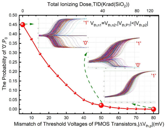
Figure 6.
Simulation results for a strong cell (), it tends to be initialized to 1 as dose increases.
For a weak cell, NMOS transistors dominate its power-on behavior as discussed in Section 3 and so the will be added step-by-step and the will always be equal to zero in simulations. The simulation results are shown in Figure 7 and Figure 8, as the mismatch deduced by TID increases, there is a modest improvement on the power-on stability of the cell, which is weaker than the situation of a strong cell.
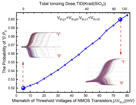
Figure 7.
Simulation results for a weak cell (), its initialized value faintly tends to 0.
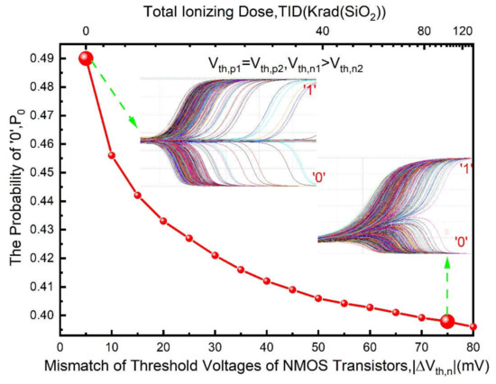
Figure 8.
Simulation results for a weak cell (), its initialized value faintly tends to 1.
Altogether, it can be concluded from above simulation results that resulted from TID effect can play an important role in enhancing the asymmetry of SRAM cells and improving their power-on stability, resulted from TID effect also works; however, its efficiency is feeble. Furthermore, it can be estimated from Figure 5 and Figure 6 that there will be significant asymmetry existing in SRAM cells when the dose accumulates to 40 Krad (SiO2) and the increases to approximately 50 mV. Of course, these are just rough estimations because the original mismatches between actual transistor pairs are different.
5. Experimental Verification
5.1. Devices and Experiment Sets
In our work, the promotion of the TID effect on the stability of SRAM PUF is explored experimentally. Irradiation experiments are performed on one type of commercial SRAM with memory capacity of 32KB. To help us carry out TID experiments more effectively, transient noise simulations have been performed on a SRAM array whose memory capacity is equal to the commercial SRAM chip and the simulation steps are similar to what is described in Section 4. The simulation results are plotted in Figure 9. The figure reveals that intra-chip hamming distance (𝐻𝐷_𝑖𝑛𝑡𝑟𝑎) drops markedly when ionization dose attains about 40 Krad (SiO2) and it will be equal to the ideal value (zero) when ionization dose reaches 180 Krad (SiO2). Of course, these values can be regarded as overestimates because the effect of has been ignored in the simulation models and so actual ionization dose will be controlled 0 Krad (SiO2)–160 Krad (SiO2) in TID experiments.
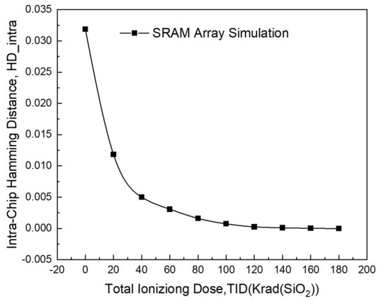
Figure 9.
SRAM array simulation results, 𝐻𝐷_𝑖𝑛𝑡𝑟𝑎 descends nonlinearly under TID effect.
The radiation experiments are carried out on Cobalt-60 Irradiation Source of Peking University in China, with the dose rate of 50 Rad (SiO2)/s. Prior to the first irradiation test, every SRAM chip’s power-on values are sampled 20 times and the two indicators ( and ) are calculated for comparison with post- irradiation situations.
The operation procedure of TID experiments can be described as Figure 10, during preparation for irradiation test, Cobalt-60 Irradiation Source remains in a Radial Well far away from earth surface and SRAM chips are placed on a bracket with supply powered off. Then the chips are powered up and Cobalt-60 Irradiation Source is raised up. Therefore the SRAM chips will hold on power-on values during irradiation until destructed by accumulated damage for a large gamma dose (e.g., 100 Krad (SiO2)), although no data pattern has been written into them before irradiation.
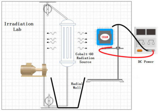
Figure 10.
Facilities for Cobalt-60 Irradiation experiments.
We take out the SRAM chips from the irradiation lab at intervals of 20 Krad (SiO2) ionization dose, then read-write tests are performed to judge if the chips still function normally, because possessing normal read-write function is a prerequisite for SRAM cells to be qualified PUF candidates. Next core step is recording the power-on data of the SRAM chips to calculate the two indicators. Note that every SRAM chip’s power-on values are sampled 20 times and every chip must be powered off for at least 15 s until next power-on cycle. As a result, charges are leaked completely and the impact of remaining data of last power-on cycle can be avoided.
5.2. Experimental Results
The above examinations are performed on five sample chips randomly chosen. The read-write test results are shown in Figure 11, it can be seen that 100 Krad (SiO2) is an important turning point and almost all the SRAM cells possess normal read-write function before being subjected to 100 Krad (SiO2) ionization dose irradiation. However, after 100 Krad (SiO2), the portion of cells unable to perform read-write function sharply increases. Therefore only the conditions below 100 Krad (SiO2) will be concerned when the two PUF performance indicators are discussed as bellow.
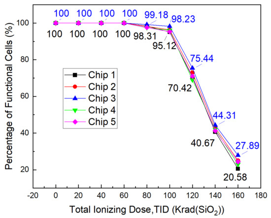
Figure 11.
Ratio of functional cells vs. total irradiation dose, 100 Krad(SiO2) is a distinct turning point.
Figure 12 shows 𝐻𝐷_𝑖𝑛𝑡𝑟𝑎 at each irradiation step. It can be seen that the nonlinear downtrend of 𝐻𝐷_𝑖𝑛𝑡𝑟𝑎 is in conformity with our simulation results. In details, 𝐻𝐷_𝑖𝑛𝑡𝑟𝑎 of all the chips is approximately equal to 0.03 before irradiation and will be reduced by two orders of magnitude when ionization dose is accumulated to 40 Krad (SiO2)–100 Krad (SiO2). That is to say the power-on data of approximately 99% cells will keep stable between different power-on cycles. It suggests that TID effect results in impressive improvement of stability.
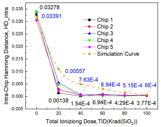
Figure 12.
𝐻𝐷_𝑖𝑛𝑡𝑟𝑎 at each irradiation step, 𝐻𝐷_𝑖𝑛𝑡𝑟𝑎 of all tested chips holds the magnitude of after 40 Krad(SiO2).
Hamming weight () representing uniformity of the power-on data at each irradiation step is displayed in Figure 13. remains slightly above 0.5 before irradiation and keeps more and more close to 0.5 under 40 Krad (SiO2). Above 40 Krad (SiO2), becomes less and less than 0.5. Considering should be as close as possible to 0.5, the accumulated ionization dose keeping uniformity close to ideal value is supposed to remain at about 40 Krad (SiO2). And the exposure time for this dose is just about 13 min at the dose rate of 50 Rad (SiO2)/s.
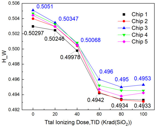
Figure 13.
at each irradiation step.
Finally, a comparison with prior works is presented in Table 1. The proposed method can enlarge mismatches of SRAM cells and hence avoid the necessity of tape-out. This method achieves more significant stability improvement by a simpler implementation compared to modifying cell structure in Reference [21]. Its exposure time is approximately 4% of aging injection suggested in Reference [24], benefitting from high energy ray from irradiation source. In addition, it has much more useful cells than preselection used in Reference [13], because the mismatches of SRAM cells in a whole chip are amplified after irradiation, while the cells with small mismatches are directly deleted in preselection.

Table 1.
Comparison with prior works.
6. Conclusions
In this work, based on the shift of transistors’ threshold voltages induced by TID effect, a novel method proven by simulations is proposed to improve the stability of SRAM PUF and then TID experiments are carried out to verify the performance of proposed scheme. The results indicate that 𝐻𝐷_𝑖𝑛𝑡𝑟𝑎 of all the tested chips can always hold on the magnitude of when ionization dose is accumulated to 40 Krad (SiO2)–100 Krad (SiO2). But the recommended ionizing dose must be selected considering the impact of TID effect on other performance indicators of SRAM PUF. Notice that 100% SRAM cells behave normal read-write function under 60 Krad (SiO2), so the recommended ionizing dose should remain no higher than 60 Krad (SiO2) and the irradiation induced damage can be kept within a minor range. On the other hand, uniformity comes nearest to the equal distribution of ‘1’ and ‘0’ when the accumulated ionization dose comes to 40 Krad (SiO2). Based on an overall consideration of the above factors, we choose 40 Krad (SiO2) to be the recommended accumulated ionization dose, which is able to confirm that the stability of SRAM PUF can be greatly strengthened without sacrificing other performance indicators. The time needed to accumulate ionizing irradiation dose of 40 Krad (SiO2) is just 13 min at the dose rate of 50 Rad (SiO2)/s.
Author Contributions
Conceptualization, X.Z. and C.J.; Data curation, X.Z.; Investigation, G.D.; Methodology, C.J. and K.G.; Project administration, L.Z. and G.D.; Software, X.Z.; Validation, X.Z. and W.F.; Visualization, X.Z.; Writing—original draft, X.Z.; Writing—review & editing, C.J., K.G., L.Z. and G.D. All authors have read and agreed to the published version of the manuscript.
Funding
This research was funded by National Natural Science Foundation of China under Grant 61904164.
Conflicts of Interest
The authors declare no conflict of interest.
References
- McGrath, T.; Bagci, I.E.; Wang, Z.M.; Roedig, U.; Young, R.J. A PUF taxonomy. Appl. Phys. Rev. 2019, 6, 011303. [Google Scholar] [CrossRef]
- Van Der Leest, V.; Van Der Sluis, E.; Schrijen, G.-J.; Tuyls, P.; Handschuh, H. Efficient Implementation of True Random Number Generator Based on SRAM PUFs. In Computer Vision; Springer Science and Business Media LLC: Berlin, Germany, 2012; Volume 6805, pp. 300–318. [Google Scholar]
- Bohm, C.; Hofer, M. Physical Unclonable Functions in Theory and Practice. In Physical Unclonable Functions in Theory and Practice; Springer Science and Business Media LLC: Berlin, Germany, 2013; pp. 16–19. [Google Scholar]
- AlAmro, M.; Mursi, K.T.; Zhuang, Y.; Aseeri, A.; Alkatheiri, M.S. Robustness and Unpredictability for Double Arbiter PUFs on Silicon Data: Performance Evaluation and Modeling Accuracy. Electronics 2020, 9, 870. [Google Scholar] [CrossRef]
- Cao, Y.; Robson, A.J.; Alharbi, A.; Roberts, J.; Woodhead, C.; Noori, Y.J.; Bernardo-Gavito, R.; Shahrjerdi, D.; Roedig, U.; Fal’Ko, V.I.; et al. Optical identification using imperfections in 2D materials. 2D Materials 2017, 4, 045021. [Google Scholar] [CrossRef]
- Liu, W.; Yu, Y.; Wang, C.; Cui, Y.; O’Neill, M.; Weiqiang, L. RO PUF design in FPGAs with new comparison strategies. In Proceedings of the IEEE International Symposium on Circuits and Systems (ISCAS), Lisbon, Portugal, 24–27 May 2015. [Google Scholar]
- Lim, D.; Lee, J.; Gassend, B.; Suh, G.; Van Dijk, M.; Devadas, S. Extracting secret keys from integrated circuits. IEEE Trans. Very Large Scale Integr. Syst. 2005, 13, 1200–1205. [Google Scholar] [CrossRef]
- Guajardo, J.; Kumar, S.S.; Schrijen, G.-J.; Tuyls, P. FPGA Intrinsic PUFs and Their Use for IP Protection. In Proceedings of the International Workshop on Cryptographic Hardware and Embedded Systems, Vienna, Austria, 10–13 September 2007. [Google Scholar]
- Maes, R.; Rozic, V.; Verbauwhede, I.; Koeberl, P.; Van Der Sluis, E.; Van Der Leest, V. Experimental evaluation of Physically Unclonable Functions in 65 nm CMOS. In Proceedings of the European Solid State Device Research Conference (SSCIRC), Bordeauz, France, 17 September 2012. [Google Scholar]
- Fruhashi, K.; Shiozaki, M.; Fukushima, A.; Murayama, T.; Fujino, T. The arbiter-PUF with high uniqueness utilizing novel arbiter circuit with Delay-Time Measurement. In Proceedings of the IEEE International Symposium of Circuits and Systems (ISCAS), Seoul, South Korea, 20–23 May 2012. [Google Scholar]
- Intrinsic ID. Intrinsic ID SRAM PUF Technology. Available online: https://www.intrinsic-id.com/sram-puf/ (accessed on 26 April 2020).
- Mispan, M.S.; Duan, S.; Halak, B.; Zwolinski, M. A reliable PUF in a dual function SRAM. Integration 2019, 68, 12–21. [Google Scholar] [CrossRef]
- Liu, M.; Zhou, C.; Tang, Q.; Parhi, K.K.; Kim, C.H. A data remanence based approach to generate 100% stable keys from an SRAM physical unclonable function. In Proceedings of the IEEE/ACM International Symposium on Low Power Electronics and Design (ISLPED), Portland, OR, USA, 27–29 August 2007. [Google Scholar]
- NXP. NXP Secures the Edge with Two Industry-First Multi-Core Arm Cortex-M33 Solutions. Available online: https://www.nxp.com/search?keyword=AN12292&start=0 (accessed on 3 August 2020).
- Intrinsic ID. QuiddiKey®. Available online: https://www.intrinsic-id.com/products/quiddikey/ (accessed on 3 June 2020).
- Microsemi. Libero SoC v11.6 Resources Archive. Available online: https://www.microsemi.com/product-directory/design-resources-archive/5086-libero-soc-v11-6-resources-archive (accessed on 10 October 2019).
- Schrijen, G.-J.; Van Der Leest, V. Comparative analysis of SRAM memories used as PUF primitives. In Proceedings of the Design, Automation & Test in Europe Conference & Exhibition (DATE), Dresden, Germany, 12–16 March 2012. [Google Scholar]
- Kiamehr, S.; Golanbari, M.S.; Tahoori, M.B. Leveraging aging effect to improve SRAM-based true random number generators. In Proceedings of the Design, Automation & Test in Europe Conference & Exhibition (DATE), Lausanne, Switzerland, 27–31 March 2017. [Google Scholar]
- Bhargava, M.; Mai, K. A High Reliability PUF Using Hot Carrier Injection Based Response Reinforcement. In Proceedings of the of International Conference on Cryptographic Hardware and Embedded Systems, Santa Barbara, CA, USA, 19–22 August 2013. [Google Scholar]
- Jang, J.-W.; Ghosh, S. Design and analysis of novel SRAM PUFs with embedded latch for robustness. In Proceedings of the Sixteenth International Symposium on Quality Electronic Design, Santa Clara, CA, USA, 2–4 March 2015. [Google Scholar]
- Okumura, S.; Yoshimoto, S.; Kawaguchi, H.; Yoshimoto, M. A 128-bit Chip Identification Generating Scheme Exploiting Load Transistors’ Variation in SRAM Bitcells. IEICE Trans. Fundam. Electron. Commun. Comput. Sci. 2012, 95, 2226–2233. [Google Scholar] [CrossRef]
- Zhang, X.; Wang, P.; Zhang, Y. Highly stable data SRAM-PUF in 65nm CMOS process. In Proceedings of the IEEE 10th International Conference on ASIC.; Institute of Electrical and Electronics Engineers (IEEE), Shenzen, China, 28–31 October 2013. [Google Scholar]
- Garg, A.; Kim, T.T.; Garg, A. Design of SRAM PUF with improved uniformity and reliability utilizing device aging effect. In Proceedings of the IEEE International Symposium on Circuits and Systems (ISCAS), Melbourne, Australia, 1–5 June 2014. [Google Scholar]
- Garg, A.; Lee, Z.C.; Lu, L.; Kim, T.T.-H. Improving uniformity and reliability of SRAM PUFs utilizing device aging phenomenon for unique identifier generation. Microelectron. J. 2019, 90, 29–38. [Google Scholar] [CrossRef]
- Xiao, K.; Rahman, M.; Forte, D.; Huang, Y.; Su, M.; Tehranipoor, M. Bit selection algorithm suitable for high-volume production of SRAM-PUF. In Proceedings of the IEEE International Symposium on Hardware-Oriented Security and Trust (HOST), Arlington, VA, USA, 6–7 May 2014. [Google Scholar]
- Mathew, S. A 0.19 pJ/b PVT-variation-tolerant hybrid physically unclonable function circuit for 100in 22nm CMOS. In Proceedings of the IEEE International Solid-State Circuits Conference, San Francisco, CA, USA, 9–13 February 2014. [Google Scholar]
- Shifman, Y.; Miller, A.; Keren, O.; Weizmann, Y.; Shor, J. A Method to Improve Reliability in a 65-nm SRAM PUF Array. IEEE Solid-state Circuits Lett. 2018, 1, 138–141. [Google Scholar] [CrossRef]
- Lee, M.; Cho, S.; Lee, N.; Kim, J. New Radiation-Hardened Design of a CMOS Instrumentation Amplifier and its Tolerant Characteristic Analysis. Electronics 2020, 9, 388. [Google Scholar] [CrossRef]
- Esqueda, I.S. Modeling of Total Ionizing Dose Effects in Advanced Complementary Metal-oxide-Semiconductor Technologies. Ph.D Thesis, Arizona State University, Tempe, AZ, USA, 2011. [Google Scholar]
- Ma, T.-P.; Dressendorfer, P.V. Phenomenological description of ionizing radiation effects. In Ionizing Radiation Effects in MOS Devices and Circuits; John Wiley & Sons: New York, NY, USA, 1989; pp. 35–43. [Google Scholar]
- Setyawan Sajim, A. Open-Source Software-Based SRAM-PUF for Secure Data and Key Storage Using Off-The-Shelf SRAM. Master’s Thesis, Delft University of Technology, Delft, The Netherlands, 2018. [Google Scholar]
- Wu, P.-C.; Yeh, C.-Y.; Tsai, H.-H.; Juang, Y.-Z. Low-frequency noise reduction technique for accelerometer readout circuit. In Proceedings of the IEEE Asia Pacific Conference on Circuits and Systems (APCCAS), Jeju, South Korea, 25–28 October 2016. [Google Scholar]


© 2020 by the authors. Licensee MDPI, Basel, Switzerland. This article is an open access article distributed under the terms and conditions of the Creative Commons Attribution (CC BY) license (http://creativecommons.org/licenses/by/4.0/).