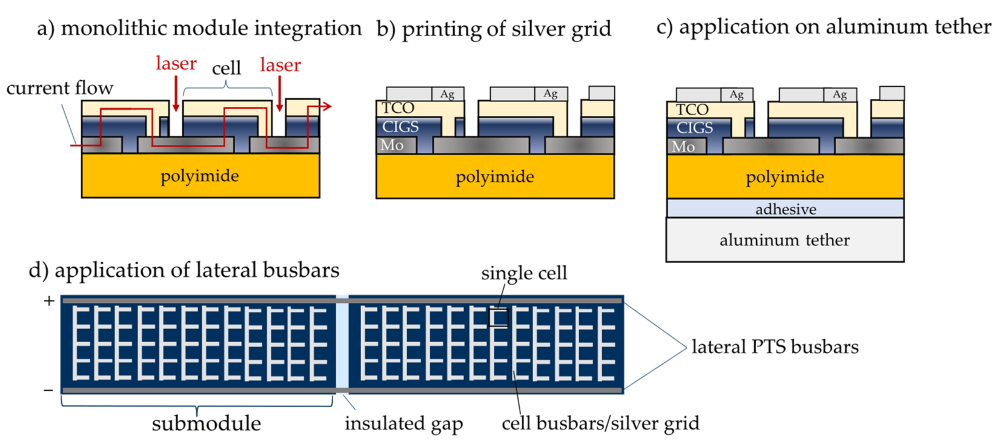
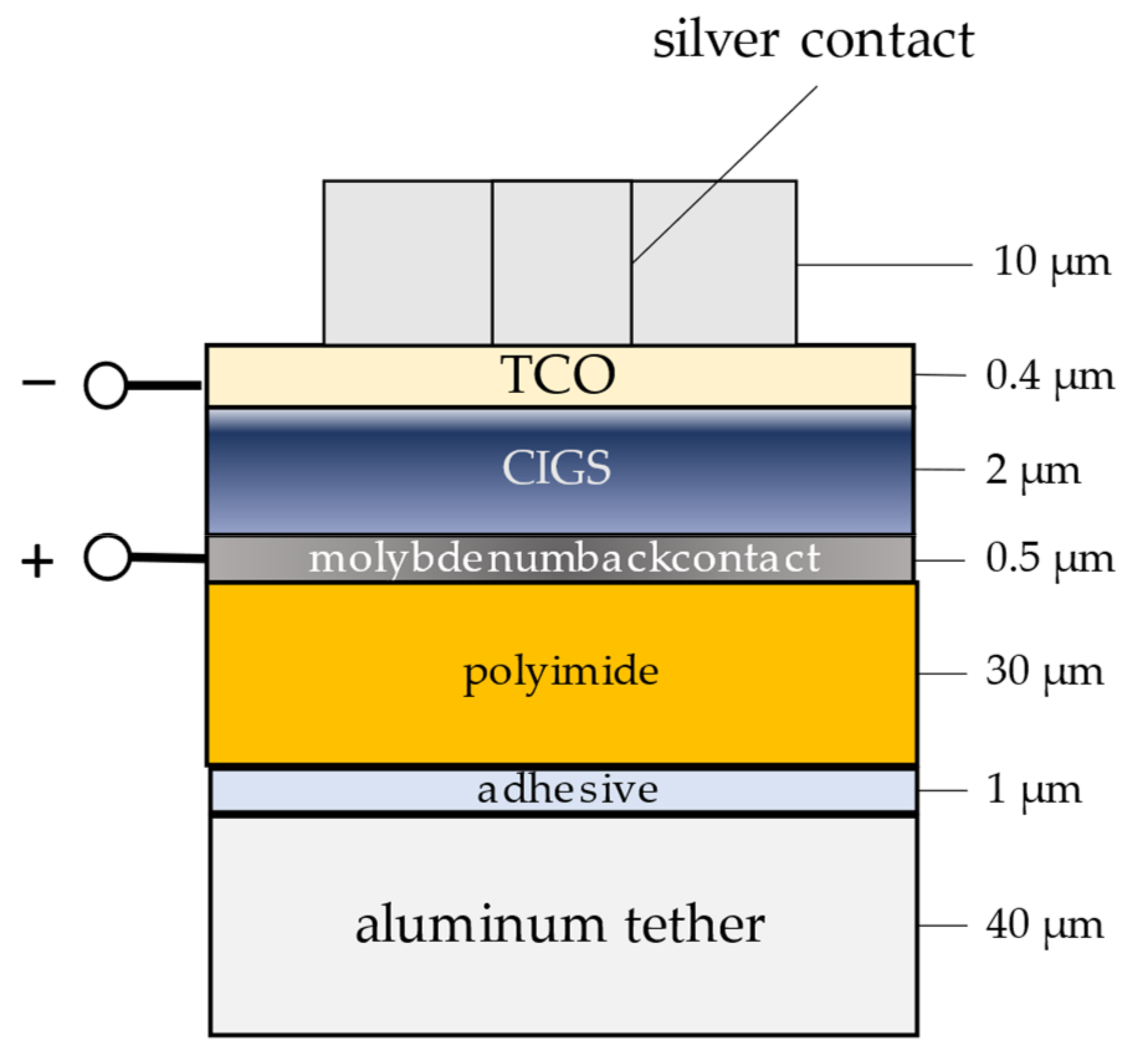
2.1. The PTS Design and PTS Samples
The PTS is integrated into the EDT, using a polyimide layer as a substrate for the thin film solar cells and as an insulating barrier to the bare aluminum tether. Typically, flexible CIGS solar cells are grown either on stainless-steel sheets with a thin film insulating glass layer or directly on polyimide sheets. Stainless-steel as an electrically conductive substrate has been discussed as a promising solution for PTS, as the EDT current could be carried by the stainless-steel layer while the glass insulator decoupled the photovoltaic circuit [
9]. In addition, CIGS solar cells on stainless-steel generally achieve higher power conversion efficiencies, due to higher process temperatures, thus leading to beneficial crystal growth [
11]. However, stainless-steel has more than twice the density of bare aluminum, a significantly lower electrical conductivity, and its use in a PTS creates the problem of joining the PTS substrate to the bare aluminum tether of the EDT. As shown in
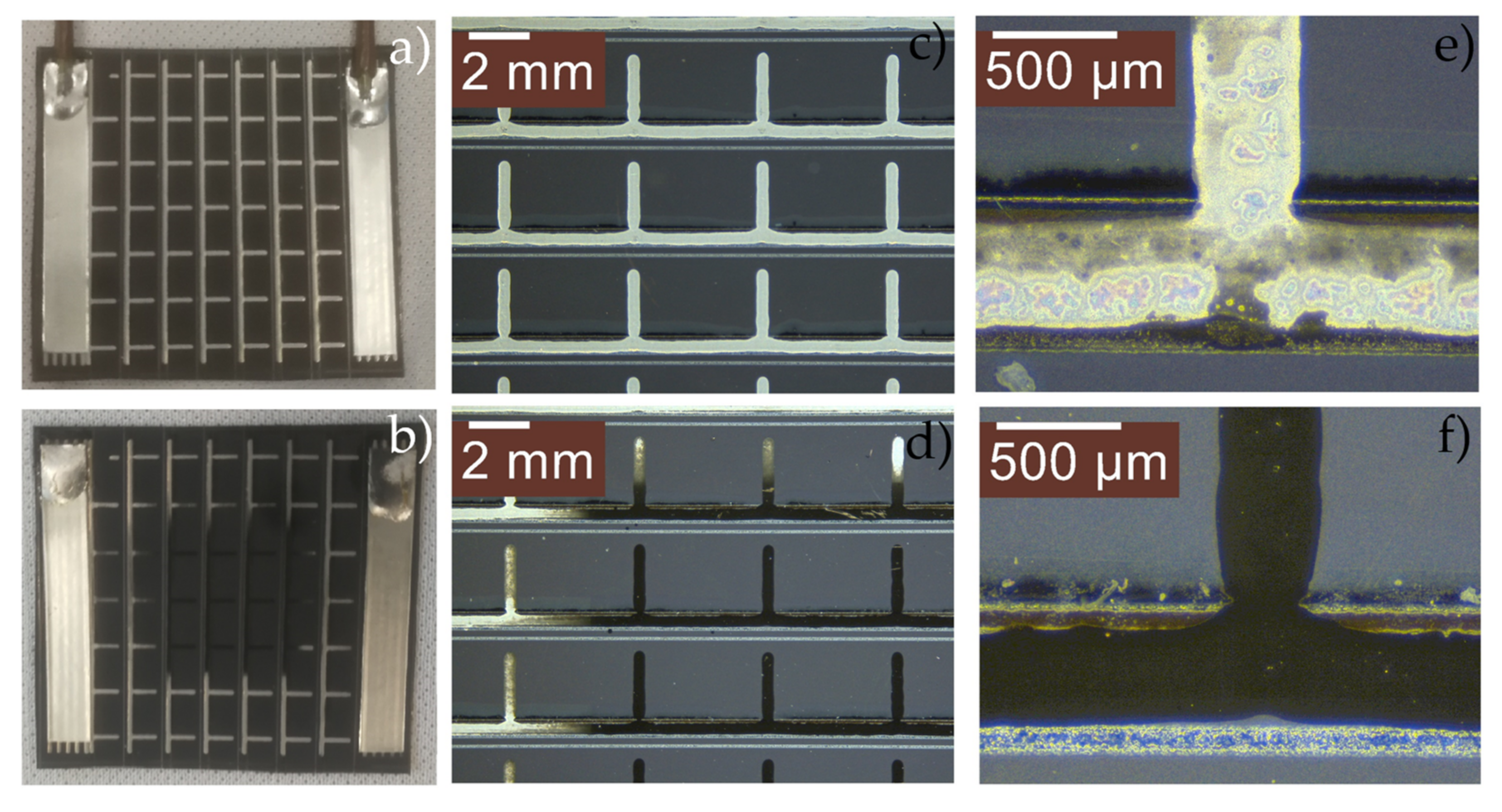
Figure 1, the PTS of this study includes a polyimide layer as both a direct substrate for the thin-film solar cells and an insulator to decouple the two electrical circuits. The cells consist of a transparent conductive oxide (TCO) front contact, in this case Aluminum-doped Zinc-Oxide (AZO), the CIGS graded absorber crystal, and a molybdenum back contact. The front contact is supported by a silver grid to enhance electron collection and to reduce ohmic losses.
Before the silver electron collecting grid is applied and the cell stack is mounted on the aluminum tether, the cell layers are patterned into submodules via monolithic integration [
12]. These patterns can be freely adapted to meet the actual use-case requirements. In this study, these submodules were designed in to have a maximum power point voltage of 28 V at 25 °C and to be connected in parallel. After monolithic integration, the submodules are applied to the aluminum tether using adhesive transfer tape. They are interconnected by two lateral busbars, which are applied after sealing to the gaps between each submodule with an insulating material (see
Figure 2). They also serve as electrical contacts to the spacecraft.
The parallel connection of the submodules to the lateral busbars is not visible from the outside and was also realized with laser structuring. The reason for this PTS architecture is a partial shading issue, resulting from torsional twisting of the PTS along the tether line after deployment. However, this torsional twisting is both detrimental and beneficial to the performance of the PTS. On the one hand, it reduces the active photovoltaic area; on the other hand, it reduces the negative effects of a sub-optimal tether orientation (e.g., when the pv area is facing away from the sun). As a result, the twisted PTS power is lower but more stable. Applying the solar cells on both sides of the tether is not feasible for two reasons. First, the solar cells have a preferred bending direction and would therefore crack if applied on both sides. Second, the electron collection capability of the bare aluminum tether would be reduced, if not completely lost, in the region of the PTS.
However, partial shading prohibits the serial connection of submodules along the tether line because the current voltage characteristic of a serial connection of solar cells or entire modules is dominated by its weakest link, and thus by the least illuminated element of the connection. If a PTS of serially connected submodules had torsional twists along the tether line, its performance would drop to zero even if only one of the submodules was in shadow. This could be avoided by adding bypass diodes to each submodule. However, they would increase the thickness of the PTS, reducing its flexibility, and making it a vulnerable but indispensable element. Instead, the PTS of this study includes submodules connected in parallel. When submodules are shaded or inside the transition zone between light and shadow, their performance drops to zero, while illuminated submodules still contribute to the total power output of the PTS. The PTS power of the parallel configuration would only decrease in proportion to the shaded photovoltaic area, instead of dropping to zero as in a serial configuration. This is an oversimplification of the process because the irradiance on the photovoltaic area changes with the angle of incidence; therefore, there are further detrimental effects of twisting. These effects are discussed in the experimental section below.
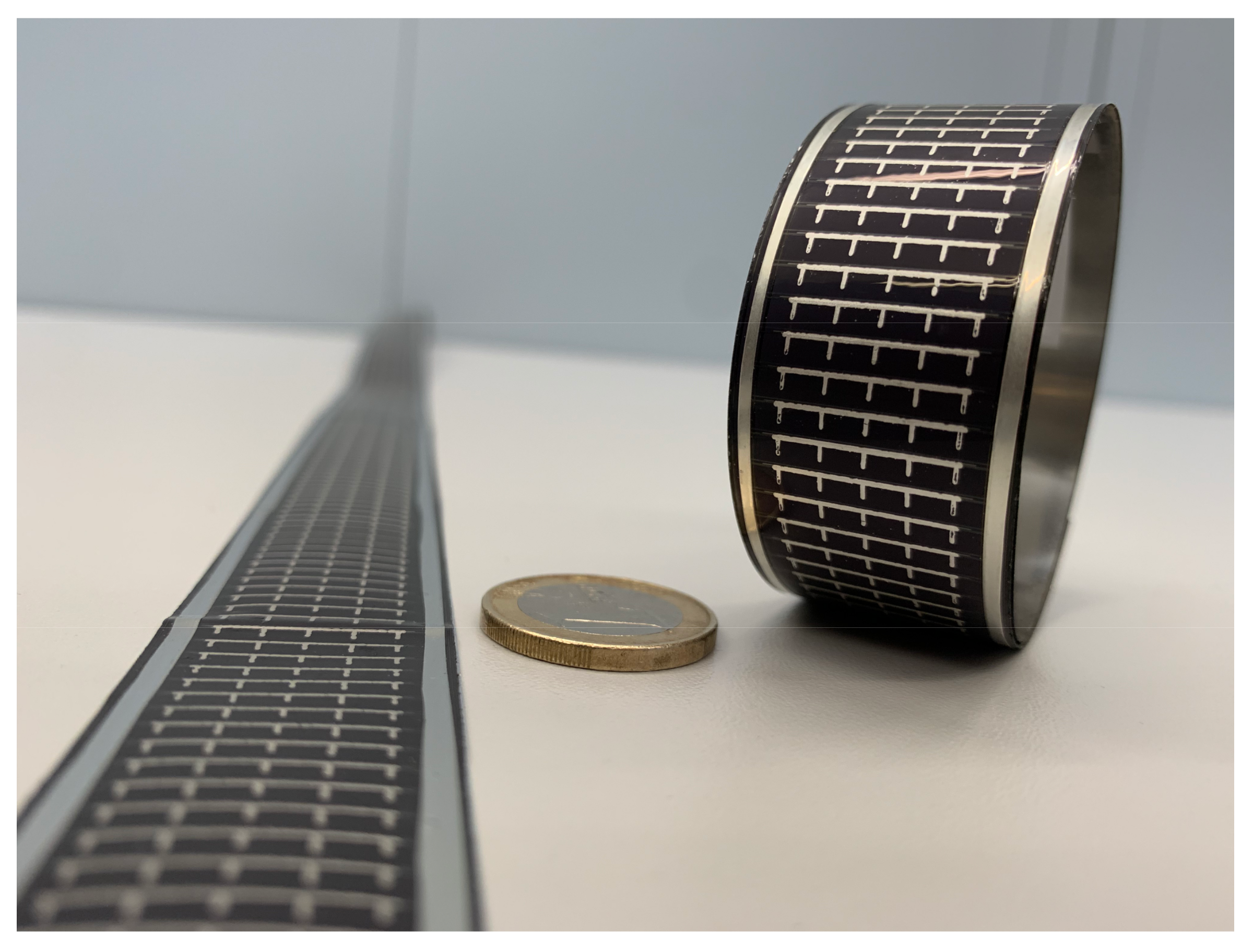
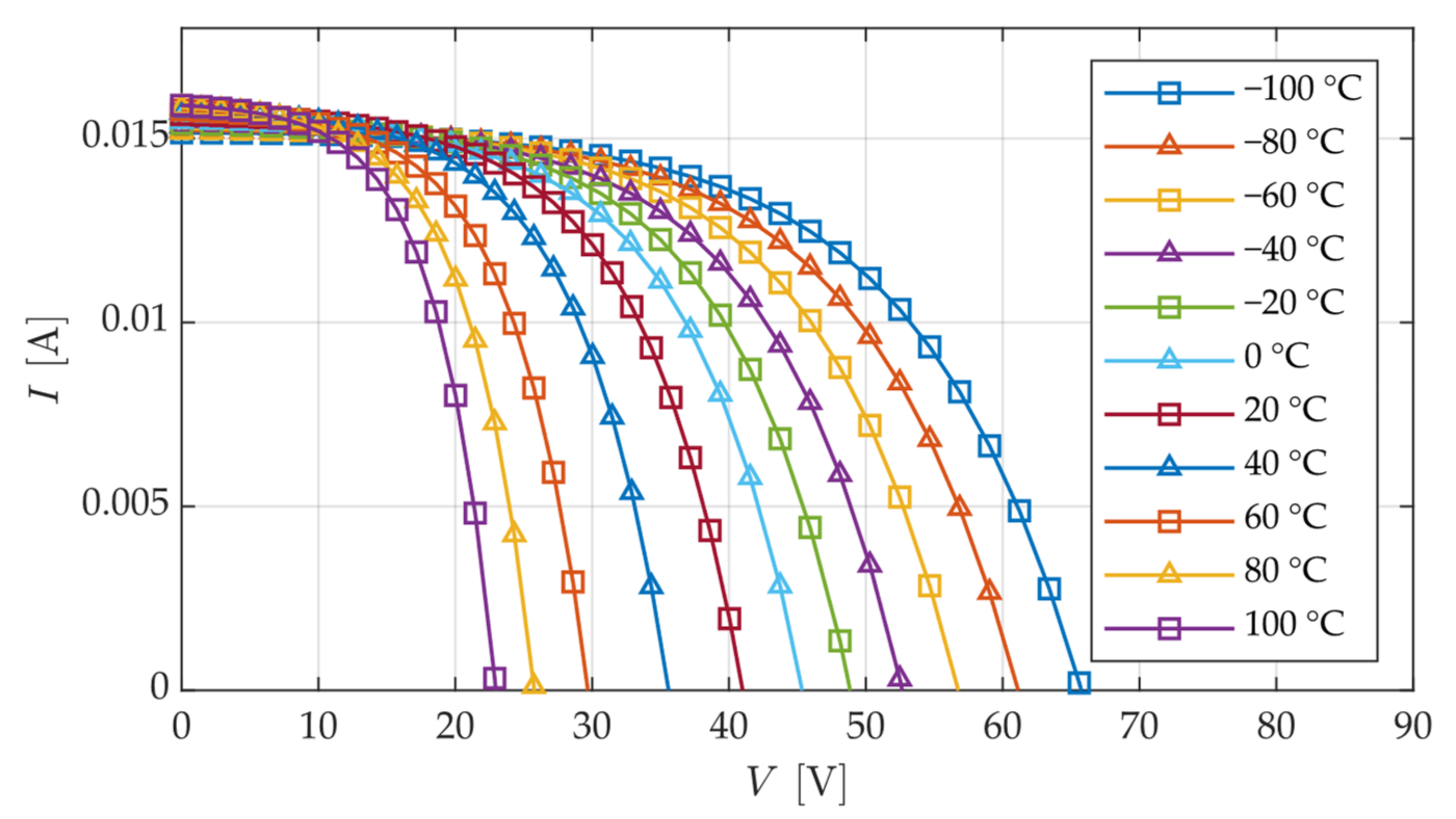
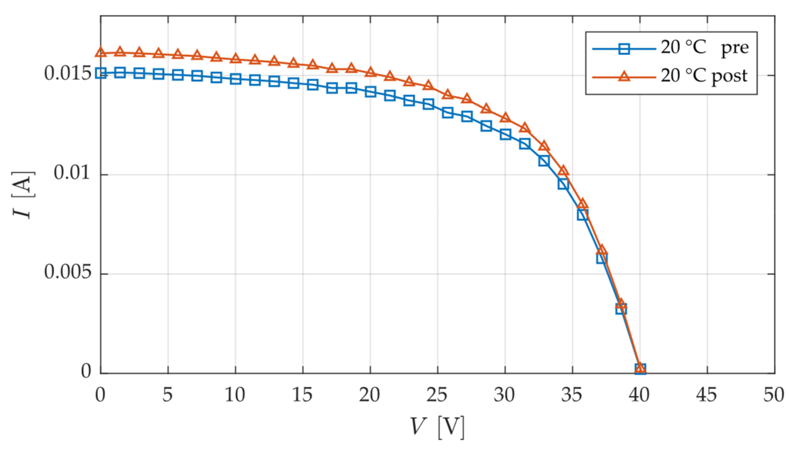
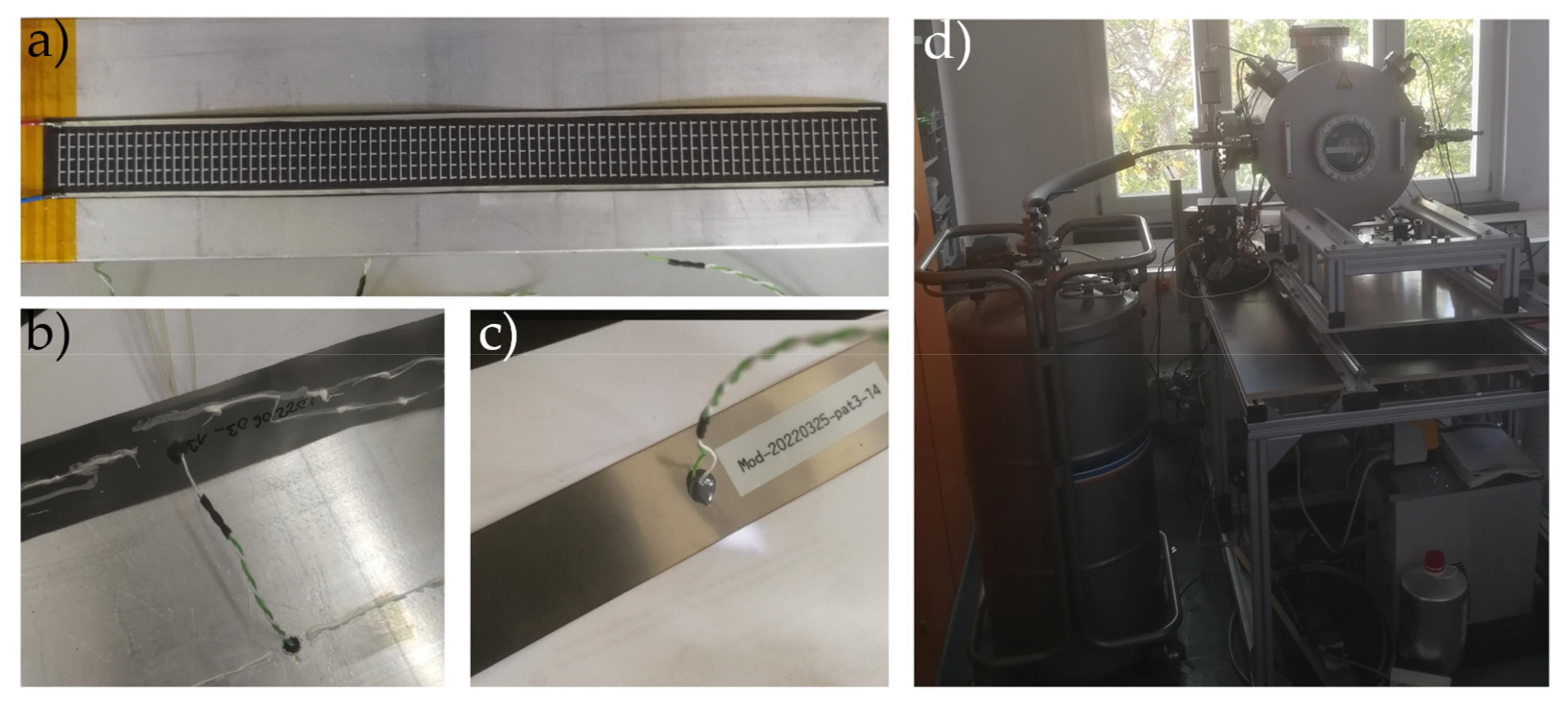
In this study, the electrical characteristics of six 25 cm long and 2.5 cm wide submodules were evaluated under the influence of vacuum and temperature. In addition, a 1.5 m long PTS sample, consisting of six submodules of the same type, which were connected in parallel, was tested against the influence of twisting.
Figure 3 shows one of the coiled-up submodules on the right side and the 1.5 m PTS sample on the left side.
These samples have a total thickness of 103 μm, including the lateral busbars. The busbars are made of a conductive copper tape 20 μm thick and 2 mm wide. Their mass per unit length is 6 g/m compared to 2.7 g/m for the bare 40 μm aluminum tether. The key parameters of the six submodules are shown in
Table 1. First, the efficiency η
0 is shown, measured with a Keithley 2420 Source Measurement Unit (SMU) under a g2voptics Sunbrick Solar Simulator (SoSi) at 25 °C and Air-Mass 0 (AM0) spectrum (1367 W/m
2). Second, the electrical parameters, open circuit voltage V
oc and short circuit current I
sc, as well as the maximum power point voltage V
MPP and current I
MPP, are presented. Third, the fill factor (FF) is presented, which is the ratio between the product of the maximum power point parameters I
MPP × V
MPP and the product of the open circuit voltage and short circuit current V
oc × I
sc and is a measure of the quality of the photovoltaic cells. In addition, the serial resistance R
s and parallel resistance R
p of each submodule are indicated, since they directly influence the FF.
The efficiencies of the submodules cannot compete with state-of-the-art CIGS module efficiencies between 12% and 15% [
10]. This is mainly due to a high serial resistance and a low parallel resistance, which increase dissipation and shunt losses, respectively. The detrimental serial resistance can be attributed to the high number of serially connected cells, whereas the low parallel resistance may be a result of the lateral PTS busbars, which cover the entire length pf the submodules and thus provide a high contact area for shunting. The average efficiency of the PTS submodules of CIGS cells on polyimide applied to a bare aluminum tether was lower than that reported for PTS submodules of CIGS cells on stainless-steel (7%), which serves as both the cell substrate and the electrical conductor for the EDT over the length of the PTS [
9].
When connecting these submodules in parallel in a PTS, it is important that they have the same or at least similar current–voltage (I-V) characteristics, so that the operating point of the overall PTS is compatible with each individual submodule. Matching the submodules at this stage of development is time-consuming and costly due to the creation of rejects by the non-optimized manufacturing process. For example, in a batch of twelve submodules, seven samples had a deviation in IMPP or VMPP of more than 5% and up to 45% from the envisaged values. Therefore, there was no well-matched and optimized PTS available yet. The 1.5 m PTS in this study consisted of poorly matched submodules and was primarily fabricated for mechanical testing, which is not the focus of this work. In addition, a dedicated solar simulator setup covering the full 1.5 m length with adequate illumination was not available. As a result, there are no reliable data available on the maximum performance of the 1.5 m PTS. However, the qualitative influence of torsional twisting on PTS performance was evaluated in a dedicated twisting setup.
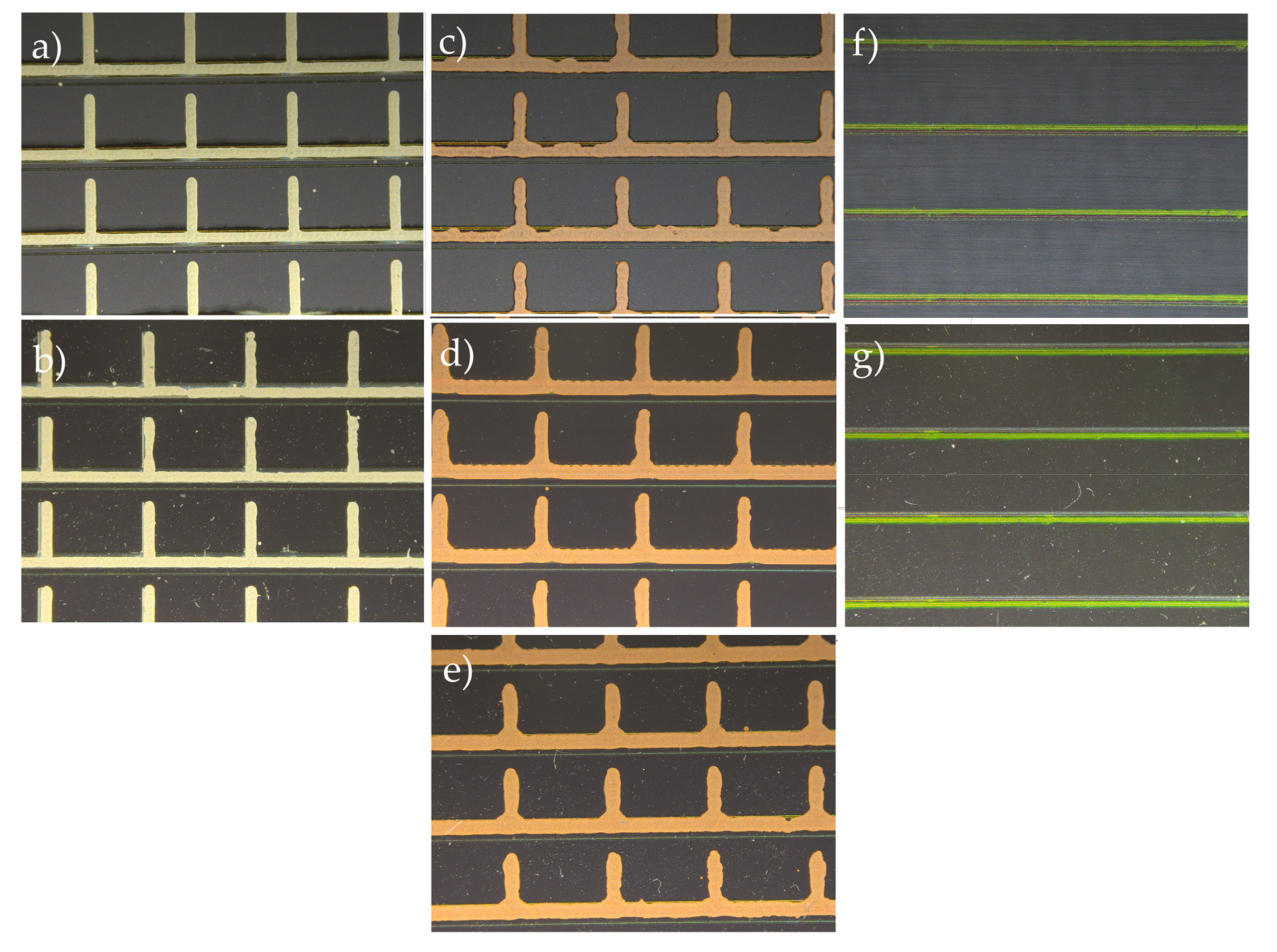
2.2. Material Demonstrators
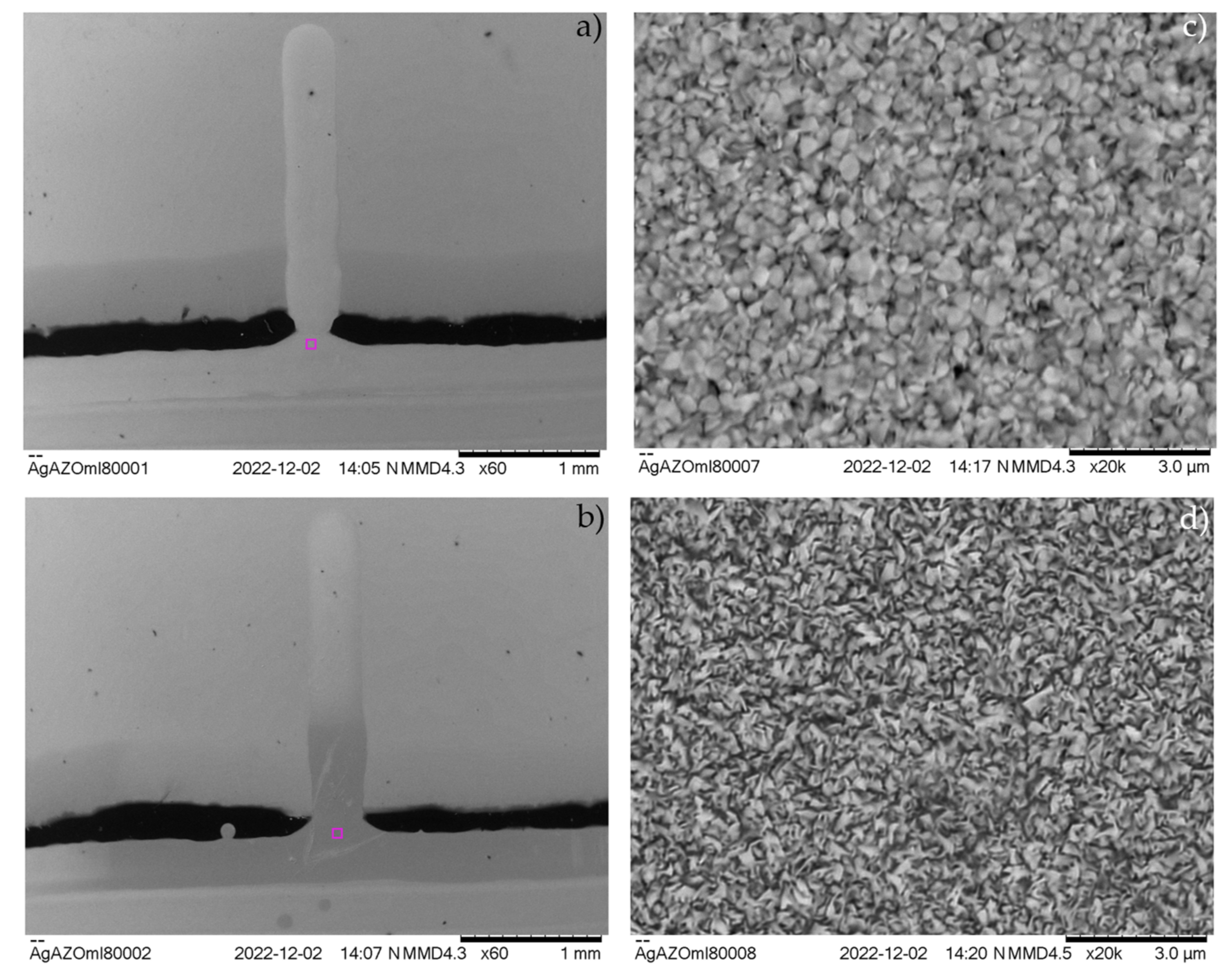
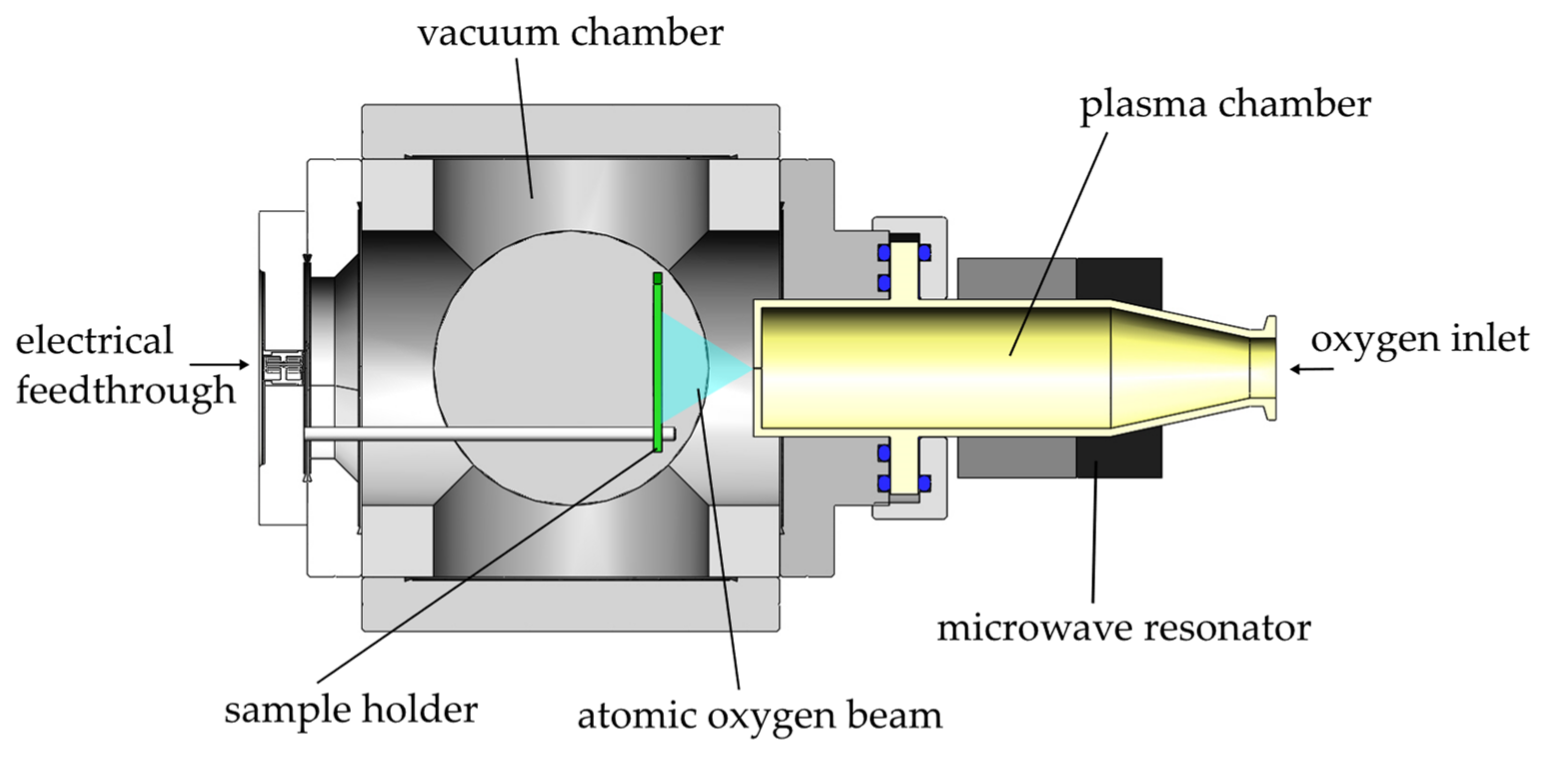
The silver electron collecting grid of the PTS is not suitable for a low Earth orbit (LEO) environment due to its susceptibility to atomic oxygen. The polyimide substrate, which is also susceptible to atomic oxygen, is protected from both sides (aluminum tether/photovoltaic cells), while the silver grid is directly exposed to atmospheric influences. Therefore, seven material demonstrators were provided and investigated to find a way to increase the robustness of the front contact against atomic oxygen. The different front contacts of the demonstrators are shown in
Figure 4.
Three approaches are considered to overcome the atomic oxygen susceptibility: using copper ink instead of silver ink for the electron collecting grid, using protective coatings, or not using an electron collecting grid at all. Therefore, the material demonstrators differed in the grid material (Silver or Copper), the coating (none, Sol-gel, CAG37 by durXtreme) and the TCO. For the latter, Aluminum-doped Zinc Oxide (AZO) and Indium Tin Oxide (ITO) were used.
Table 2 summarizes the different material combinations and shows the average efficiency of the samples at standard test conditions (STC). The samples had a square shape with a side length of 35 mm and did not contain a polyimide layer. The solar cells of all material demonstrators were deposited on stainless-steel.
The highest average efficiency (7.93%) was achieved with material combination 3 (Cu/AZO, no coating). Material combinations 5 and 6 showed the lowest efficiencies (4.74%, 5.28%), indicating the positive influence of the electron collecting grid. The influence of the coatings on the mean efficiency was not clear, as they had either a positive (no. 2 and 7) or negative effect (no. 4 and 5).
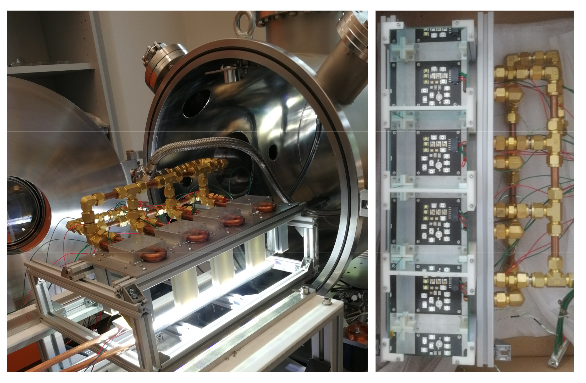
2.3. Solar Simulator (SoSi) Setup
The self-built SoSi (
Figure 5) was designed to illuminate an area of 32 cm × 8 cm on a thermal plate at a distance of 10 cm inside a vacuum chamber, allowing temperature control of the illuminated samples and vacuum exposure. The light source was based on light emitting diodes (LEDs) and consisted of four LED clusters, each consisting of 22 LEDs with 16 different peak wavelengths ranging from 270 nm to 1100 nm (see
Appendix A). Each cluster was surrounded by four square-shaped SEA-UV broadband surface mirrors from Präzisions Glas & Optik with the intention of homogenizing and guiding the light. The design of the light source was based on the works of Mohan et al. [
13] and Linden et al. [
14]; however, it was less elaborate due to lower measurement uncertainty requirements. The LEDs were soldered to aluminum printed circuit boards (PCB) mounted on liquid-cooled aluminum heat sinks. The aluminum thermal plate was flushed with either water or liquid nitrogen (LN2). In addition, two 10 W heating foils were applied to the back of the thermal plate to control its equilibrium temperature, which was influenced by the liquid cooling, the irradiance of the SoSi, and the heaters.
According to the IEC standards for simulator performance requirements [
15], this solar simulator was rated Spectral Match (SM) Class B in the wavelength range 400 nm to 1000 nm for the AM0 spectrum, Spatial Uniformity (SNU) Class C in an area of 4 cm × 32 cm and a Temporal Stability (TS) of Class A. The spectral irradiance of the SoSi was determined using a Qmini RGB Photonics (Wide UV) spectrometer in combination with the current signal from a calibrated FDS100-CAL photodiode from Thorlabs. The spectral irradiance E(λ) [W/m
2nm] of the SoSi was calculated using Equation (1) with the measured normalized spectrum S
n(λ) [1/nm] of the SoSi, the spectral sensitivity R
ph(λ) [A/W], the current output I
ph [A], and the active area A
ph [m
2] of the photodiode.
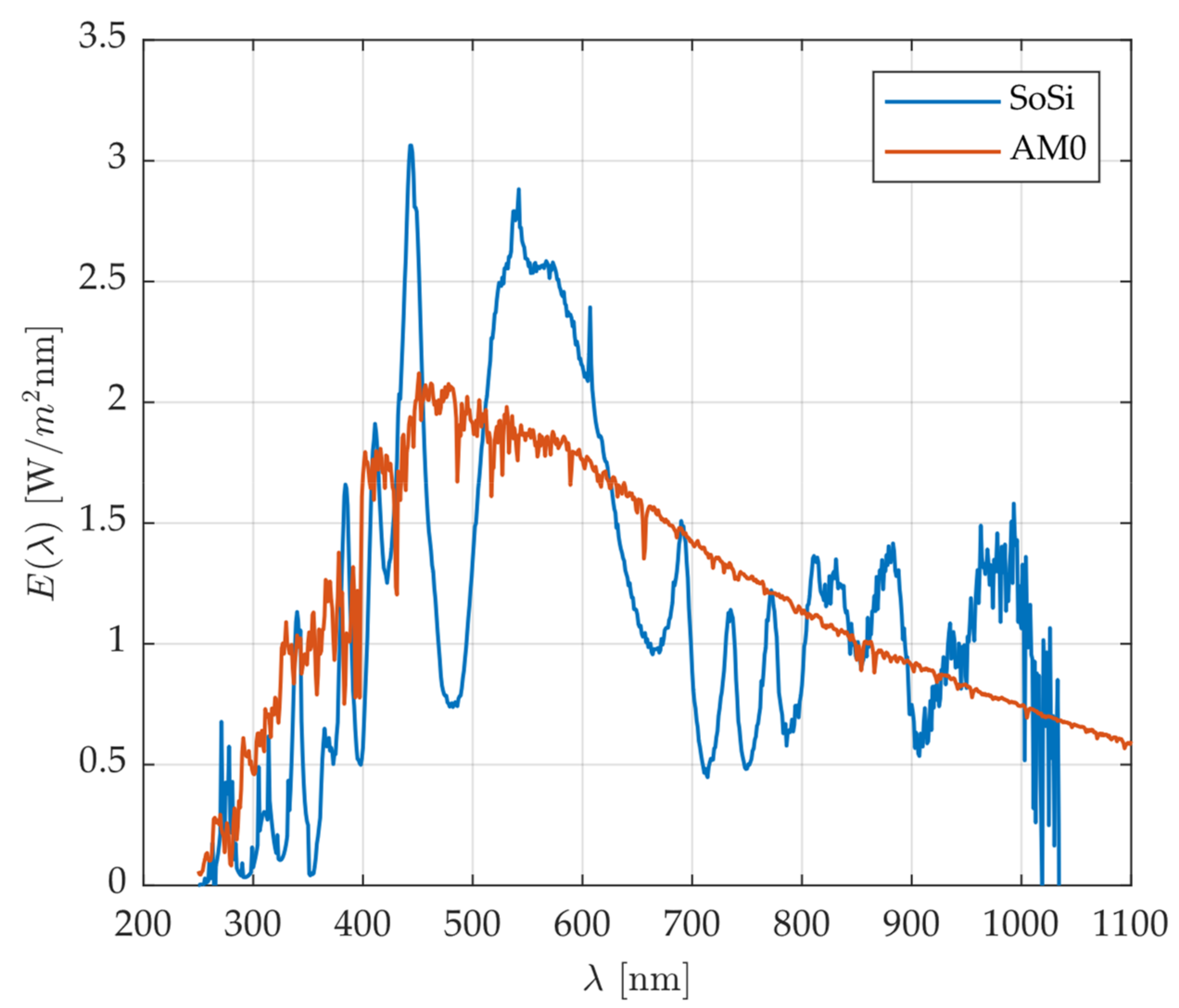
The spectral irradiance of the SoSi is shown in
Figure 6 in comparison to the AM0 spectrum of the Sun. The measurement was made in the center of the 8 cm × 8 cm test area at a distance of 10 cm below one of the LED clusters.
The spectrometer used for this measurement covers a wavelength range from 250 nm to 1000 nm. Therefore, insufficient data were collected above 1000 nm. In
Table 3, the irradiance of the SoSi in the wavelength range 200 nm to 1100 nm is compared to the irradiance of the Sun with an interval width of 100 nm.
In the range from 200 nm to 1100 nm, the SoSi therefore only achieves SM class C, while in the 400 nm to 1000 nm range, it achieves class B with a maximum deviation of 40% in the 700–800 nm interval. The total irradiance of the SoSi in the full wavelength range is 10% lower than the irradiance of the sun in the same range.
The spatial non-uniformity (SNU) is a measure of how uniformly the irradiance of the SoSi is distributed in the test plane. It is calculated using Equation (2) according to IEC [
15].
In Equation (2), E
max and E
min are the maximum and minimum irradiances measured in the test plane, respectively. The SNU of the SoSi was determined by measuring the photocurrent of the calibrated FDS100-CAL photodiode at 64 equidistant points in the 8 cm × 8 cm test plane below each LED cluster. This results in an 8 × 8 matrix that can be plotted as a contour plot.
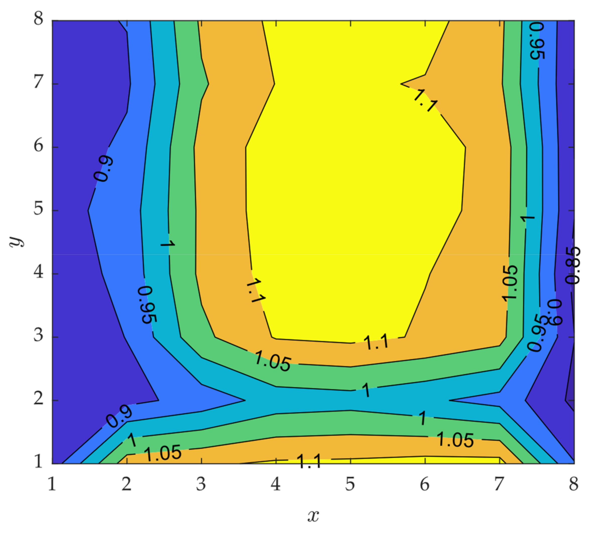
Figure 7 shows a contour plot of the spatial distribution of the irradiance in the 8 cm × 8 cm test plane under a LED Cluster. At each position, the measured local irradiance E′ is compared to the mean irradiance E
m in the plane as the ratio E′/E
m. The contour lines indicate zones of similar irradiance. Each boundary indicates its numerical threshold value. For example, the zone inside the 1.1 boundary means that the local irradiance is higher than the mean irradiance by a factor between 1.1 and 1.15. However, this plot does not directly visualize the spatial uniformity of the irradiance, but only provides a descriptive impression. According to Equation (2), the SNU of the 8 cm × 8 cm plane is 15.1% and thus a failure of the SNU criterion. However, in the zone of
Figure 7 between x = 3 and x = 7 and in the entire y-range, the SNU is 9.7% which is sufficient for class C. The spatial distribution of irradiance was nearly the same for all four LED clusters, so that the distribution of irradiance for the full 8 cm × 32 cm test plane can be obtained by stringing together the plot of
Figure 7 four times in the y-direction.
The temporal stability (TS) was determined by continuously measuring the photocurrent of the FDS100-CAL photodiode with a Keithley 2450 SMU. The photodiode was placed in the center of one of the 8 cm × 8 cm test planes. After 30 min of measurement, the TS was determined to be 0.06%, fulfilling the class A criterion.
Due to the non-optimized spectral match, the spatial non-uniformity of the irradiance and the non-collimated light source of the self-built solar simulator, it is not suitable for precise calibrations and measurements in the specific field of solar cell development. However, it was suitable for a qualitative analysis of the electrical characteristics of the PTS at different temperatures in a limited area of 4 cm × 32 cm.
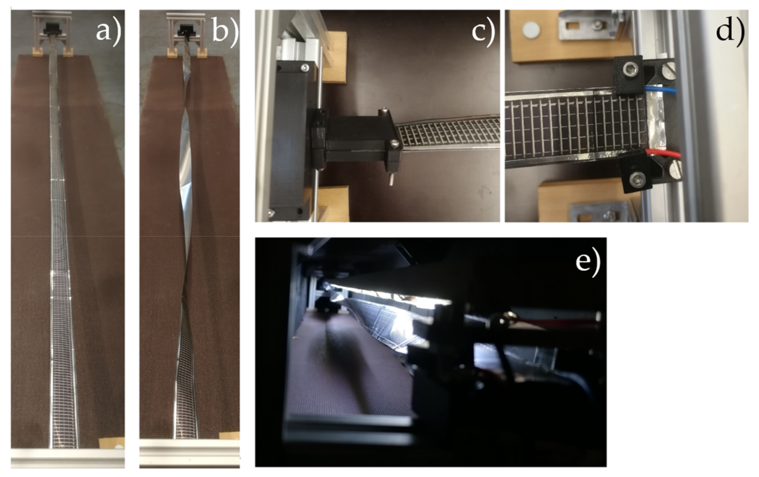
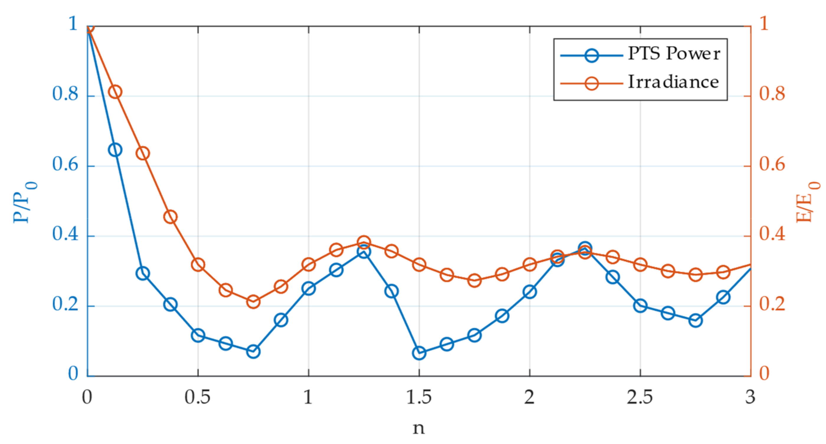
2.5. Twisting Setup
The PTS is expected to twist arbitrarily along the tether line in space due to the EDT-deployment. Since the tether can be thought of as a torsion spring, this twisting will vary with time (number of twists per length).The irradiance on a surface depends on the angle of light incidence. If the surface of the PTS is assumed to be uniformly twisted along its length, the irradiance on that surface is reduced by a factor of 1/π (0.32) compared to the case, in which the entire PTS surface is orthogonal to the incident light over the entire length. In addition, the reflection behavior also depends on the angle of light incidence. The submodules of the PTS will therefore experience suboptimal and constantly changing illumination conditions, which will affect the overall I-V characteristic of the PTS.
A setup was constructed to qualitatively evaluate the influence of torsional twists on the performance of the PTS. The setup is shown in
Figure 9. It features two mechanical fixings for the 1.5 m PTS. One of the fixings can be freely rotated to simulate the twisting. The other has an electrical connection to a Keithley 2450 SMU.
The PTS was clamped between these two fixings and placed under a light source inside a cardboard box that was completely painted black to reduce light reflections and external light incidence. The light source consisted of a cool white LED strip with a radiant power of 550 Lumen/m which equals around 4.4 W/m. As a rough estimate, the irradiance on the PTS at a distance of 3 cm from the light source was determined to be 42 W/m2, considering an LED aperture half angle of 60°. The light source was not collimated.
The normalized irradiance
along the twisted PTS with a length
of 1.5 m can be described as in Equation (3) for this experimental setup.
is the undisturbed irradiance of the light source on an orthogonal surface and n is the number of twists over the entire length. The cosine relation results from the fact that the PTS is fixed on one side so that the PTS surface is always orthogonal to the light sourceat this point of fixation. Equation (3) can be used to plot the irradiance on the photovoltaic surface of the PTS against the longitudinal coordinate Las, a function of the number of twists n. Integrating E/E0 over the entire length of the PTS for different n and considering only the positive share of the graph gives the percentage of radiant power received by the twisted PTS compared to a PTS without any twists (n = 0). This would lead, e.g., to a percentage of 63.71% for n = 0.25, 31.93% for n = 1 or 38.25% for n = 1.25. This model was used to evaluate the experimental results presented below and to assess whether the power output of an evenly twisted PTS can be simply described with a loss factor of 1/π or whether additional considerations need to be made.


