Abstract
In this paper, simulation modeling was carried out using Sentaurus Technology Computer-Aided Design. Two types of high electron mobility transistors (HEMT), an AlGaN/GaN/AlGaN double heterojunction and AlGaN/GaN single heterojunction, were designed and compared. The breakdown characteristics and damage mechanisms of the two devices under the injection of high-power microwaves (HPM) were studied. The variation in current density and peak temperature inside the device was analyzed. The effect of Al components at different layers of the device on the breakdown of HEMTs is discussed. The effect and law of the power damage threshold versus pulse width when the device was subjected to HPM signals was verified. It was shown that the GaN HEMT was prone to thermal breakdown below the gate, near the carrier channels. A moderate increase in the Al component can effectively increased the breakdown voltage of the device. Compared with the single heterojunction, the double heterojunction HEMT devices were more sensitive to Al components. The high domain-limiting characteristics effectively inhibited the overflow of channel electrons into the buffer layer, which in turn regulated the current density inside the device and improved the temperature distribution. The leakage current was reduced and the device switching characteristics and breakdown voltage were improved. Moreover, the double heterojunction device had little effect on HPM power damage and high damage resistance. Therefore, a theoretical foundation is proposed in this paper, indicating that double heterojunction devices are more stable compared to single heterojunction devices and are more suitable for applications in aviation equipment operating in high-frequency and high-voltage environments. In addition, double heterojunction GaN devices have higher radiation resistance than SiC devices of the same generation.
1. Introduction
With the continuous advancement of technology, the modern aviation sector faces increasingly complex and severe electromagnetic radiation challenges [1]. As a prominent representative of the new generation of aircraft, electric vertical take-off and landing (eVTOL) vehicles, with their unique vertical takeoff and landing capabilities and efficient energy utilization, are expected to play a pivotal role in future urban air transportation. However, the heavy reliance of eVTOL on advanced electronic systems and communication technologies makes them vulnerable to microwave radiation impacts [2,3].
High-power microwave (HPM), as the primary generation form, has undergone rapid development in recent years, playing a unique role in various fields such as military applications, biomedicine, imaging technology, and material processing [4,5,6,7,8]. As a medium for satellite communications and broadband wireless network transmission, data communication can be provided more rapidly and stably. However, the electronic equipment of aircraft is exceptionally sensitive and fragile due to these strong electromagnetic radiation capabilities, severely affecting flight safety. Gallium nitride is used as a wide-bandwidth semiconductor with a unique wide band gap (3.4 eV) [9], high critical electric field, and high electron saturation velocity [10]. This makes it an excellent power radio-frequency device that is more suitable for applications in high-frequency, high-temperature, and high-voltage environments, and it is has become the preferred core unit for the new generation of aircraft. Gallium nitride high electron mobility field effect transistors (GaN HEMT) have become a research hotspot in the field of microwave power devices. Therefore, it is of utmost importance to investigate the impact of high-intensity radiated fields on novel aviation nanodevices and their underlying mechanisms, which holds significant theoretical and practical implications for ensuring flight safety and promoting the sustained development of next-generation aircraft technologies.
Electromagnetic environmental effects at the aircraft’s whole and equipment levels have been studied by a large number of teams [11,12], but the chips inside equipment are equally one of the core problems that cause the failure of aircraft. In this paper, the p-GaN gate cap structure is used to realize enhanced HEMT devices, due to its excellent aero-material properties. Currently, while numerous teams are devoting efforts to the research of device processes and structural characteristics, the impact of high-power microwaves on devices is often overlooked. For instance, as mentioned in reference [13], doping magnesium (Mg) into the p-GaN gate cap layer has been employed to improve the instability of the device threshold voltage. However, achieving the desired p-type conductivity requires a significant amount of Mg doping, which may introduce excessive defects and impurities, thereby affecting the migration properties and thermal stability of the device. Reference [14] proposed a novel analytical model by incorporating a half-bridge structure. Nevertheless, this structure renders the performance of GaN devices highly susceptible to temperature variations, thus reducing stability. To date, the impact of these experimental devices under high-voltage or high-power microwave conditions has not been taken into account. Consequently, research on the combination of p-GaN HEMT and electromagnetic environmental effects holds significant importance in this context. Among contemporary device materials, silicon carbide (SiC) is renowned for its exceptional breakdown electric field (3.0 MV· cm−1) and radiation resistance (1 × 10⁹–10 rad), stemming from its stable composite crystal structure, which stands out in areas such as breakdown characteristics, high frequency, and radiation resistance [15]. Nevertheless, despite SiC devices’ outstanding performance in numerous aspects, gallium nitride (GaN) devices have been found to exhibit superior characteristics, boasting a breakdown electric field approximately 1.2-times higher and a radiation resistance nearly 10-times greater than SiC devices [16].
To make a device work efficiently in a high-frequency environment, some researchers have adopted methods such as varying gate length or incorporating field plate structures. However, this approach can lead to an increase in input capacitance, exacerbated current collapse effects, short-channel effects, and other issues [17,18]. Additionally, some scholars have performed special treatments on the surface of HEMTs to enhance the breakdown performance of the device. Nevertheless, an improper treatment may result in the introduction of new surface states and defects [19]. Based on these issues, the above problems can be effectively avoided by double heterojunction devices, allowing better high-frequency devices [20,21].
In this paper, a novel aviation nanodevice, the AlGaN/GaN/AlGaN double heterojunction HEMT device structure is designed and compared with a conventional single heterojunction GaN HEMT device. The thermal damage mechanism and breakdown characteristics of the two devices were derived by injecting high-power microwaves until the device burnt out. Compared with the single heterojunction, double heterojunction HEMT devices had high domain-limiting characteristics. The overflow of carriers from 2DEG into the buffer layer was effectively suppressed, and the internal temperature distribution of the device was improved. Subsequently, the carrier migration rate was increased, and the leakage current was reduced. Moreover, the switching and breakdown characteristics of the device were improved. In response to the increasingly complex electromagnetic environment and the growing integration of avionics and electrical systems, a novel nanodevice, more suitable for application in aircraft operating at high frequencies and voltages is proposed in this paper from the perspective of aviation safety.
The main contributions of this paper are summarized as follows:
- A novel aviation nanodevice is designed in this study. The double heterojunction GaN HEMT device model established in this paper is a unique improvement and design based on the established and mature traditional GaN HEMT device model. The reliability of the device is ensured. The new improved design also meets industry standards. This improved design enhances the breakdown characteristics. The characteristics and principles of the breakdown resistance of double heterojunction devices were derived and confirmed through a comparative analysis method.
- The electromagnetic environmental effects of aviation nanomaterials are investigated in this paper. This paper focuses on a principled study to obtain the damage mechanism and thermal breakdown process of the device. The breakdown time of the device was used as a pivotal indicator, and the distribution of current density and temperature inside the device at different time points was investigated. The often overlooked Al component is investigated in this paper and the effect of the Al component on the breakdown of the device is studied.
- The electromagnetic sensitivity of aviation nanodevices to HPM signals was studied. The damage relationship of high-power microwave signals with different parameters with the device was obtained. Moreover, fitting equations with regularity were obtained.
The remainder of this paper is organized as follows: Section 2 describes the construction of the device model. The device parameters, physical properties, and circuit models are presented separately. The correctness of the device and the reliability of the simulation are guaranteed. Section 3 details the simulation verification. The electromagnetic induction strengths and damages of single heterojunction and double heterojunction GaN HEMT devices under HPM signal conditions were studied. The methodology, laws, and analysis are included. Experiments and literature are cited to verify the consistency of the simulation results. The specificity of the task in this section is demonstrated by the fact that this paper is different from previous methods and that frequently neglected structures are studied. The conclusions are given in Section 4.
2. Model Building
2.1. Device Models
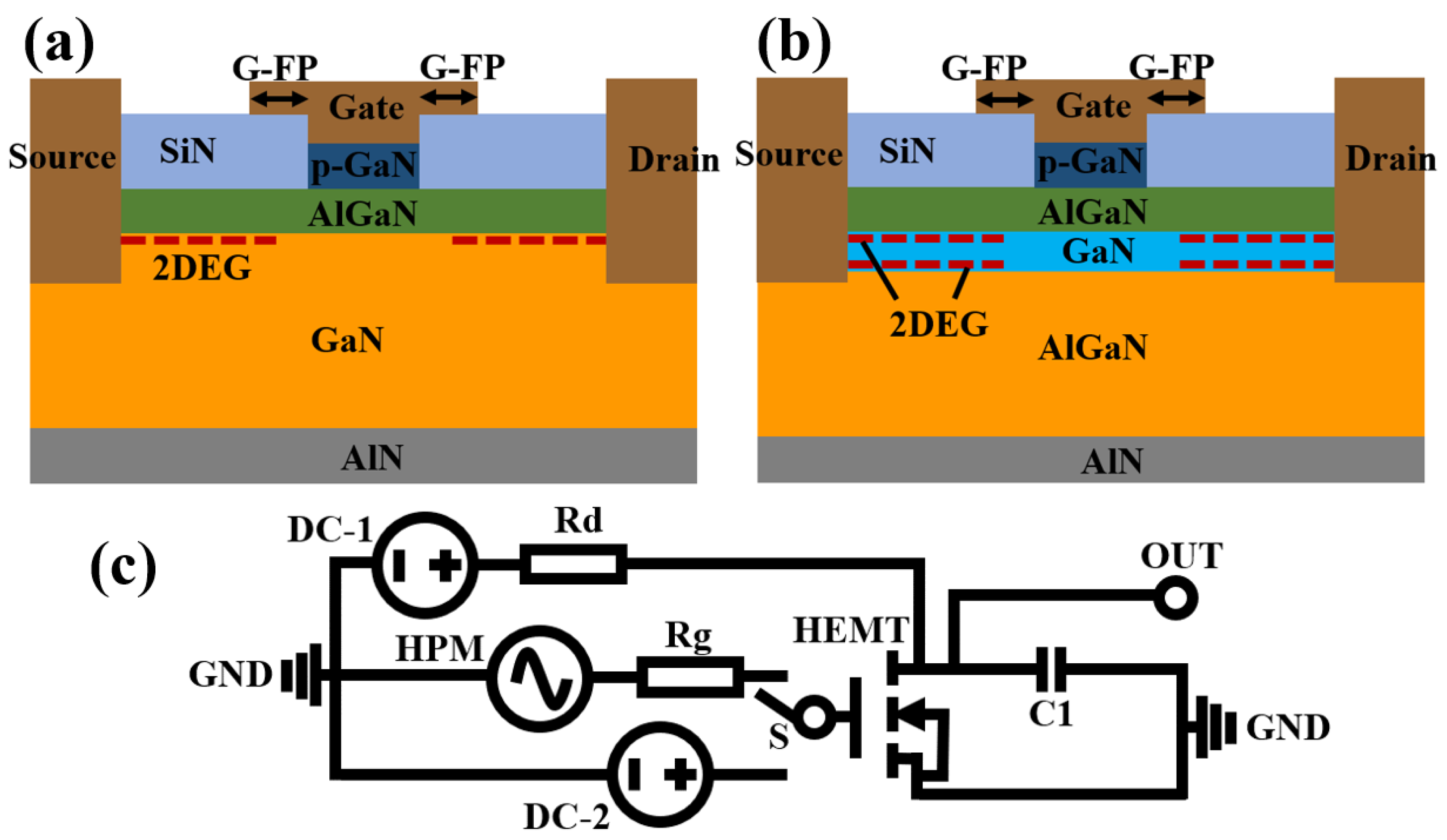
In this paper, the Sentaurus Technology Computer-Aided Design (Sentaurus-TCAD) platform was used to build a device simulation model and signal injection circuit. The structural parameters of the device are shown in Table 1. Figure 1a shows the single heterojunction AlGaN/GaN HEMT device structure. In this paper, the wurtzite structure of GaN crystals was adopted, with the atomic arrangement continuously repeating as Ga-N-Ga-N along the C-axis (0001) direction, thereby maximizing the stability of the device. Furthermore, the device exhibits a GaN polarity due to this growth direction, and this polar structure finds widespread application in practical scenarios. The thickness of the AlN as the device substrate was 10 nm. The thickness of the GaN buffer layer was 2.01 m, the arsenic atoms were selected for uniform N-type doping, and the doping concentration was 1 × 1014 cm−3. The thickness of the AlGaN barrier layer was 15 nm, arsenic atoms were selected for uniform N-type doping with a doping concentration of 1 × 1018 cm−3, and the Al component was Al0.23Ga0.77N. The thickness of the SiN passivation layer was 0.2 m. The thickness of the p-GaN gate cap layer was 0.11 m, and boron atoms were selected for uniform P-type doping with a doping concentration of 3 × 1017 cm−3. The lengths of the gate, drain, and source were 1.0 m, 0.5 m, and 0.5 m, respectively; the gate–source distance and the gate–drain distance were 3.0 m and 3.0 m, respectively; and the lengths of the field plate structures (G-FPs) at both ends of the gate were 0.5 m and 0.5 m, respectively. The metal gate/p-GaN layer formed the Schottky barrier. The gate was the Schottky impedance, and the Schottky work function for the source and drain was set to 4.3. Considering the practical application after packaging, the thermal contact temperature was set around the substrate: 300 K, and other boundaries were set as insulation. Figure 1b shows the AlGaN/GaN/AlGaN double heterojunction GaN HEMT device structure. Compared to Figure 1a, a new GaN channel layer was added, the thickness was 0.01 m, and arsenic atoms were selected for uniform N-type doping, and the doping concentration was 1 × 1015 cm−3. The thickness of the AlGaN buffer layer was 2.0 m, and arsenic atoms were selected for uniform N-type doping with a doping concentration of 1 × 1014 cm−3, and the Al component was Al0.05Ga0.95N. The rest of the conditions were the same as in Figure 1a.

Table 1.
Structural parameters of GaN HEMT devices.
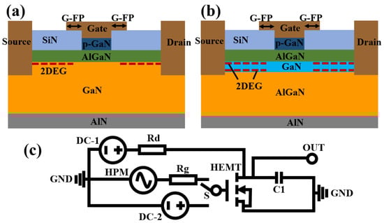
Figure 1.
Schematic structure of GaN HEMT device. (a) Conventional AlGaN/GaN single heterojunction structure, (b) AlGaN/GaN/AlGaN double heterojunction structure, and (c) simulated circuit model used for the device.
2.2. Physical Models
To obtain a more realistic device model, the process defects and physical properties present in GaN HEMT devices were taken into account in the modeling process. Physical models related to this were incorporated. High-power microwaves were used as an external condition in this paper. Therefore, the Canali model was introduced as the mobility model in the high-intensity electric field:
where represents the low-field mobility; represents the driving field; represents the saturation velocity; and the exponent varies with temperature.
The solution is carried out with electrons as an example, and the same for holes to obtain the following equations. The thermionic emission model was used to deal with the distribution of electrons at the surface of the heterojunction at the thermodynamic temperature. The interface condition is written as:
where represents the current density of electrons; represents the effective mass of electrons; represents the emission velocity of hot electrons at the interface; represents the temperature of electrons; represents the energy of the conduction band; and > 0. Considering that avalanche breakdown occurred in the device, a hydrodynamic model for temperatures was introduced to replace the traditional temperature distribution model, and the energy balance equation and energy flux equation for solving the lattice temperature T and carrier temperature are listed here:
where denotes the vector potential energy of the curl state ; and can change convective contribution and the diffusive contribution; represents the thermal conductivity. The polarization effect is a non-negligible physical defect in GaN HEMT devices. A simple polarization model is provided by the Sentaurus-TCAD platform:
where X, Y, and Z represent the coordinate directions of the device; stands for spontaneous polarization effect; stands for piezoelectric polarization; , , , and stand for piezoelectric coefficient and elasticity coefficient, respectively; stands for strain lattice constant; a stands for unstrained crystalline constant; and relax is the relaxation parameter [22,23]. In addition to this, trap effects and other physical models were included in the model.
2.3. Circuit Models
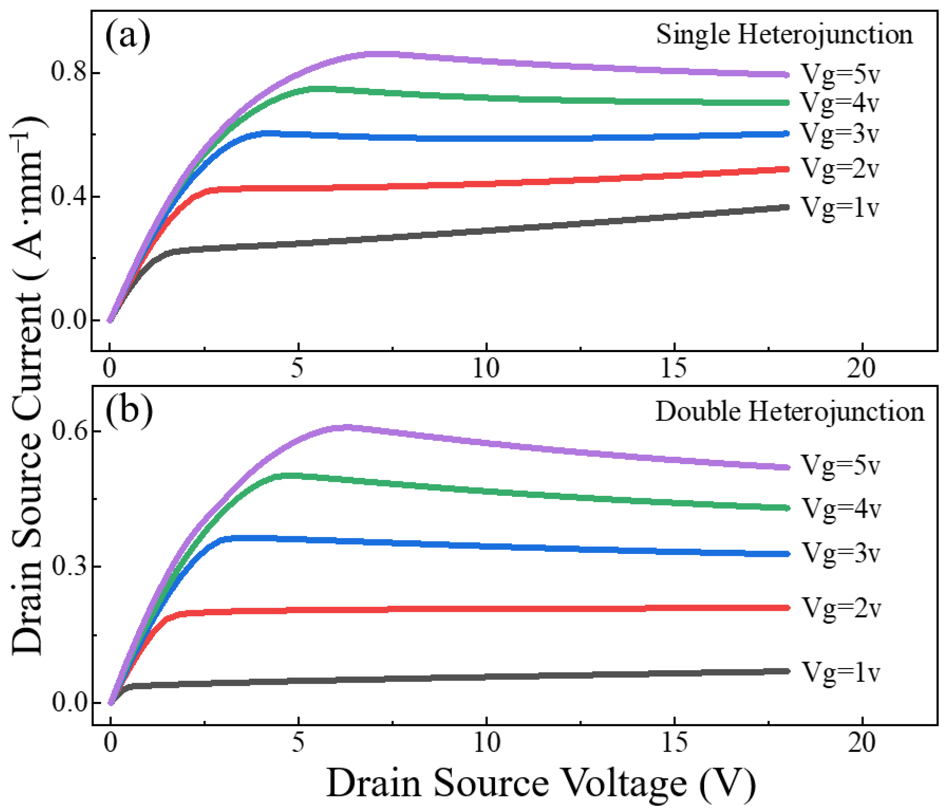
The simple analog signal injection circuit in Figure 1c was built by SPICE, where DC–1 is the drain DC bias voltage source; DC–2 is the gate DC bias voltage source; HPM is a high-power microwave signal injected from the gate; Rd is the drain bias resistor; C1 is the decoupling capacitor; Rg is the gate input resistor; and S is the single-pole, double-branch switch on the gate, which is connected to the HPM signal source, and the gate DC bias voltage source (DC–2) are connected. Figure 2 shows the IdVd transmission characteristic curve of the HEMT, demonstrating the relationship between the voltage and current at the drain when the gate DC voltage is constant. According to Figure 2, the amplitude of the selected HPM should not be less than 2 V. Moreover, the correctness of the device model is proven by the IdVd transmission characteristic curve.

Figure 2.
Transmission characteristic curves of the devices. (a) single heterojunction device, (b) double heterojunction device.
3. Results and Analysis
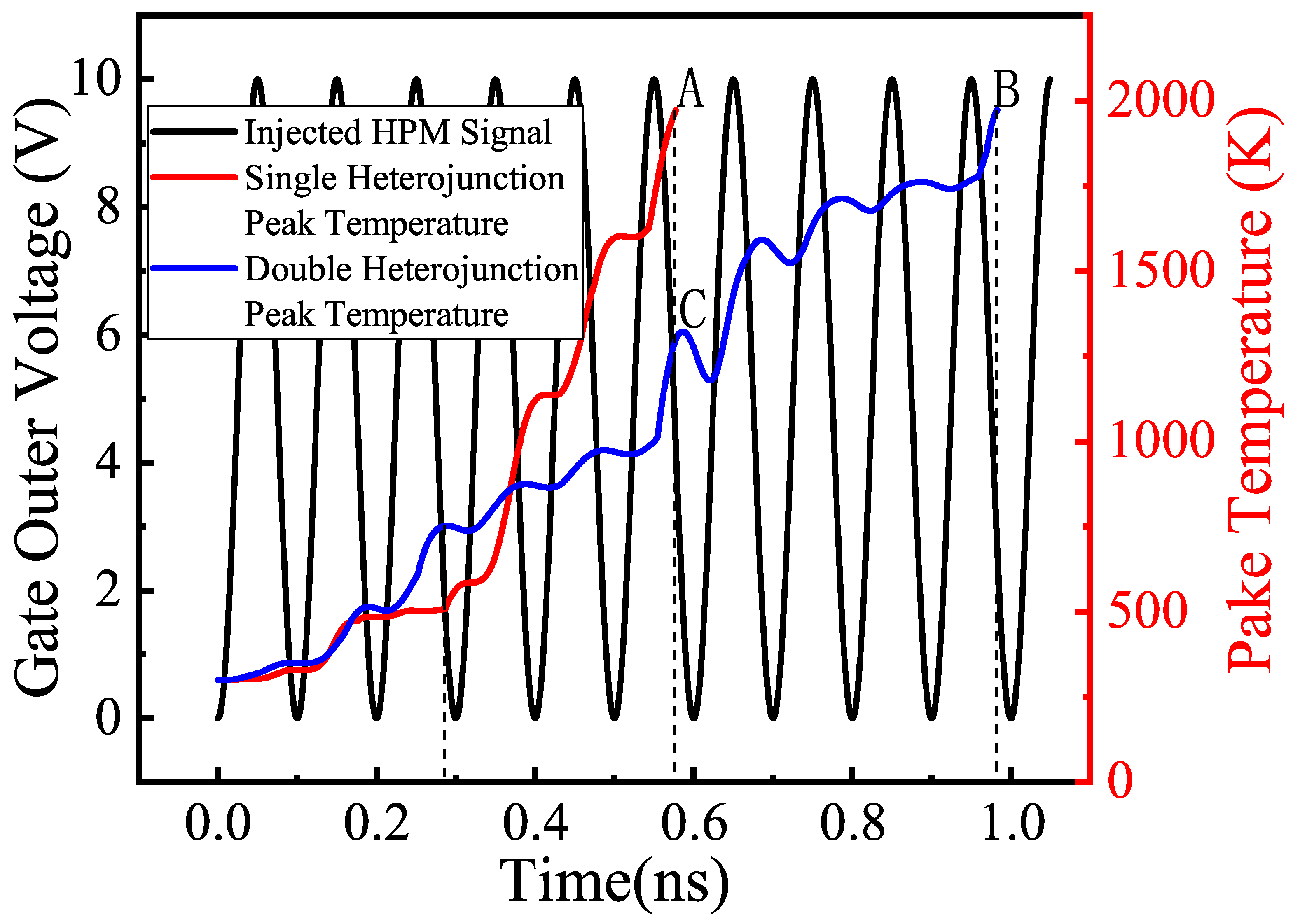
The commonly used X communication band was selected as the injected microwave signal. A single-pole, double-branch switch (S) at the gate of the device was connected to the HPM signal source, and the circuit was energized. The HPM signal source was set to continuously inject 10 GHz, 47 dBm high-power microwaves of similar sinusoidal form at the gate. Reproducibility verification was conducted multiple times, and the results were consistent. The HPM injection signal shape is given in Figure 3. In addition, when the internal temperature of the HEMT device reached 1975 K, the lowest melting point of GaN material, this was used as the basis for judging that thermal breakdown had occurred in the device. Extracting the simulation results, point A (0.5776 ns) was the breakdown moment of the single heterojunction HEMT device; point B (0.9831 ns) was the breakdown moment of the double heterojunction HEMT device; and point C and point B were the same moment, which was the comparison point of the double heterojunction HEMT device. The variation in the peak temperature inside the device with time is shown in Figure 3, where the peak temperature rise of the device was accelerated when the injected HPM signal was high, and the peak temperature rise of the device was slowed down when the injected HPM signal was low. The internal peak temperature and the injected signal changed at the same frequency. This was determined by the speed of the electrons injected by the HPM versus the rate of transfer of electrons within the device. The rate of the former was much greater than the rate of the latter; therefore, energy was accumulated and the device eventually broke down. Compared to single heterojunction HEMT devices, double heterojunction HEMT devices had a slower temperature rise, longer breakdown time, and greater resistance to breakdown.
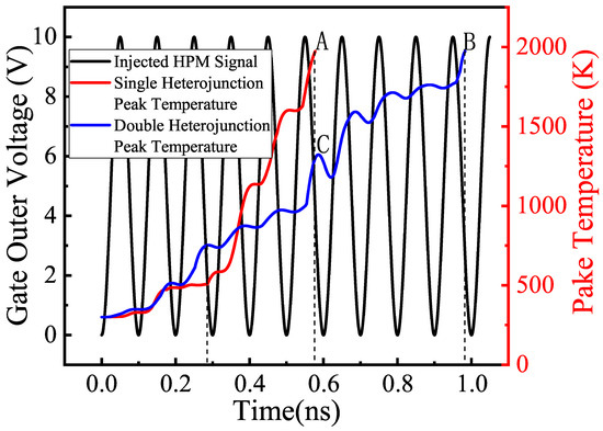
Figure 3.
HPM injection signal versus peak temperature inside the device over time.
3.1. Physical Characteristics of the Device
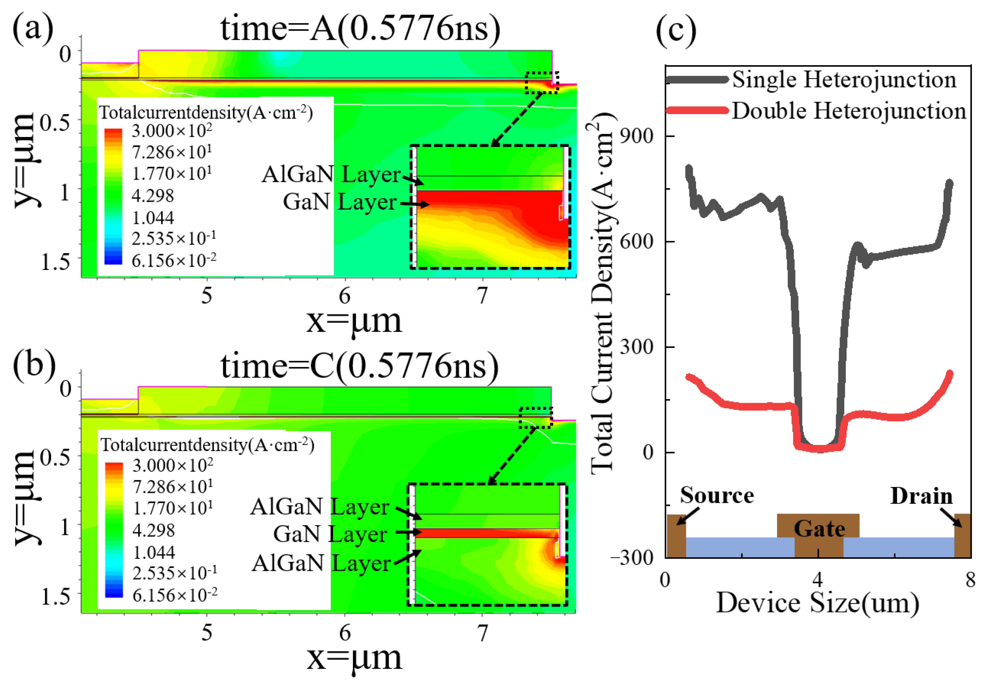
The current density was taken as the best representation of the intensity of current flow, which directly affects the speed and distribution of carrier motion and hence the migration characteristics of a semiconductor. Figure 4 shows the local distribution of current density inside the two devices at moments A and B. Compared to the 2DGE characteristics of the single heterojunction device in Figure 4a, the carriers in Figure 4b are concentrated in the GaN channel layer, with a more pronounced gradient distribution with the buffer layer. Moreover, the diffusion current near the p-gate was reduced. This was due to the fact that the AlGaN/GaN/AlGaN double heterojunction formed unique quantum wells that confined the carriers to move near the inner surfaces of the top and bottom sides of the channel layer. The distribution of current densities at the channel locations of the two devices was investigated and obtained as shown in Figure 4c. The current density distribution of the double heterojunction was more uniform and stable, which was owing to the motion speed and distribution of the carriers being directly affected by the magnitude of the current density, and hence the mean free path of the carriers was affected. On both sides of the gate, the current density in the channel of the double heterojunction device was lower, the mean free path was smaller, and the stability of the device transmission performance was enhanced. Subsequently, the mean free path of the carriers was raised, and the device began to be affected by the hot electron emission current. Since the hot electron emission current density was positively correlated with temperature and independent of the applied voltage [22], accelerating the increase in the device temperature, this was more likely to cause a breakdown. Therefore, the high domain-limiting characteristics of the double heterojunction permitted the electron injection efficiency to be increased, the transport efficiency to be improved, and the leakage current to be reduced. Therefore, the switching characteristics, breakdown characteristics, and stability of the device were improved.
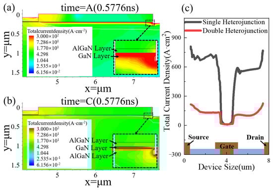
Figure 4.
Local distribution of current density inside the device at moments A and B. (a) Moment time = A (0.5776 ns) for the single heterojunction device, (b) moment time = C (0.5776 ns) for the double heterojunction device, and (c) the distribution of current densities at the channel locations of the two devices being transected.
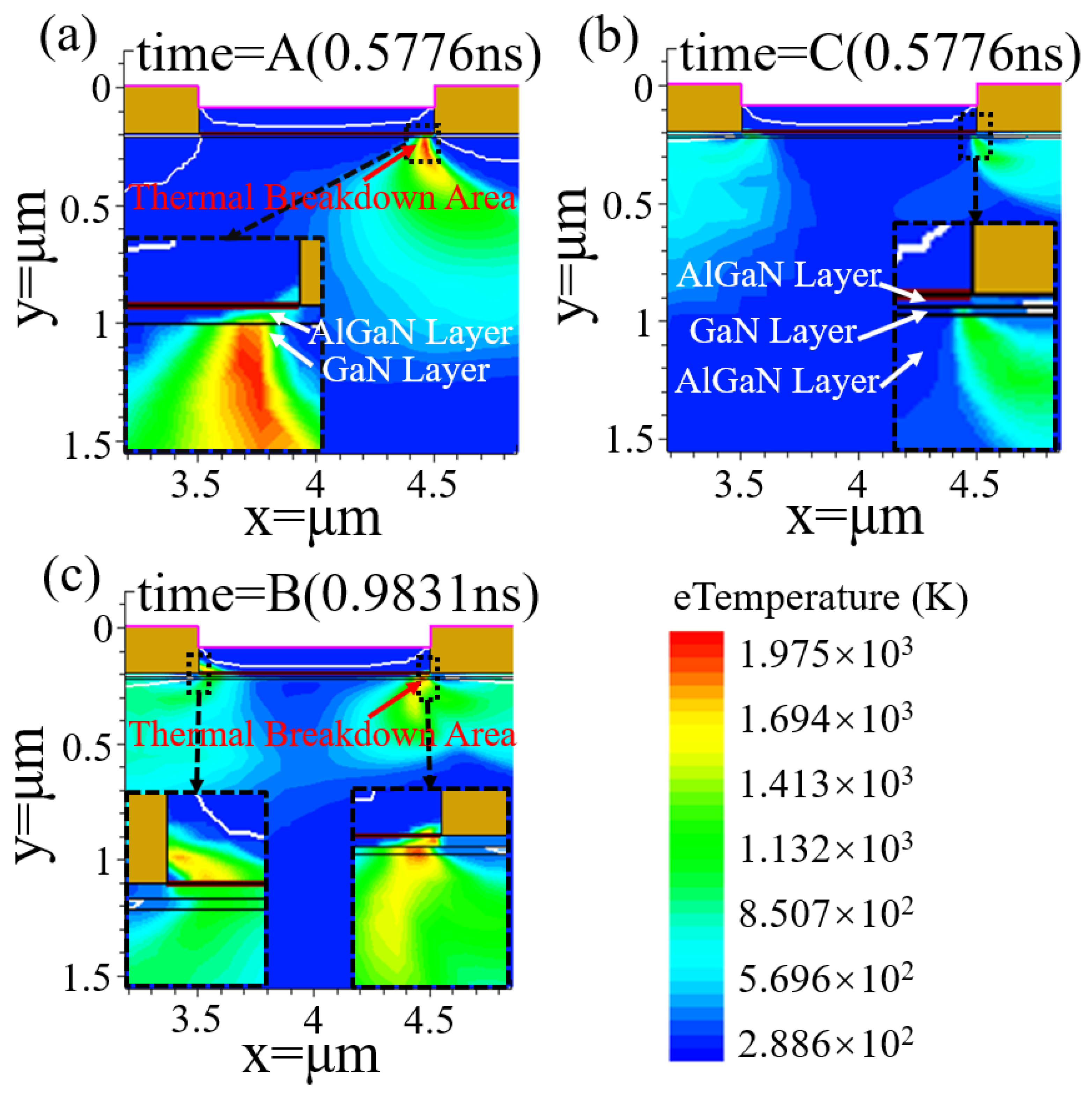
The thermal instability was caused by the structural defects at the column faces of the p-gate junction, such that the heat generated around it was continuously absorbed in each signal cycle. Due to the short pulse width and fast frequency of the input HPM signal, the conduction of the internal temperature of the device to the surroundings was less than the rate of heat generation, and the thermal accumulation effect was caused by the repetition of pulses [24]. As shown in Figure 5a, inside the single-heterojunction HEMT, the thermal breakdown occurred at the column surface of the right junction of the p-gate and the upper region of the GaN buffer layer at moment A (0.5776 ns). Inside the double heterojunction HEMT in the same period, the heat was dispersed equally on both sides of the gate (Figure 5b). The temperature at this point was gently increased until breakdown (B(0.9831 ns) moment), which occurred at the column surface of the right junction of the p-gate, and in the region around the channel. At the same time, the column surface of the left junction reached the critical threshold for breakdown (Figure 5c). In summary, the double heterojunction could effectively inhibit the 2DEG in the channel from being spilled into the buffer layer, the internal temperature distribution of the device was improved, which enhanced the breakdown characteristics of the device. In addition, the area near the carrier channel below the p-GaN HEMT gate is one of the most fragile and breakdown-prone parts of the device.

Figure 5.
Local distribution of the internal temperature of the device at moments A, B, and C. (a) Moment A of the single heterojunction device, (b) moment C of the double heterojunction device, and (c) moment B of the double heterojunction device.
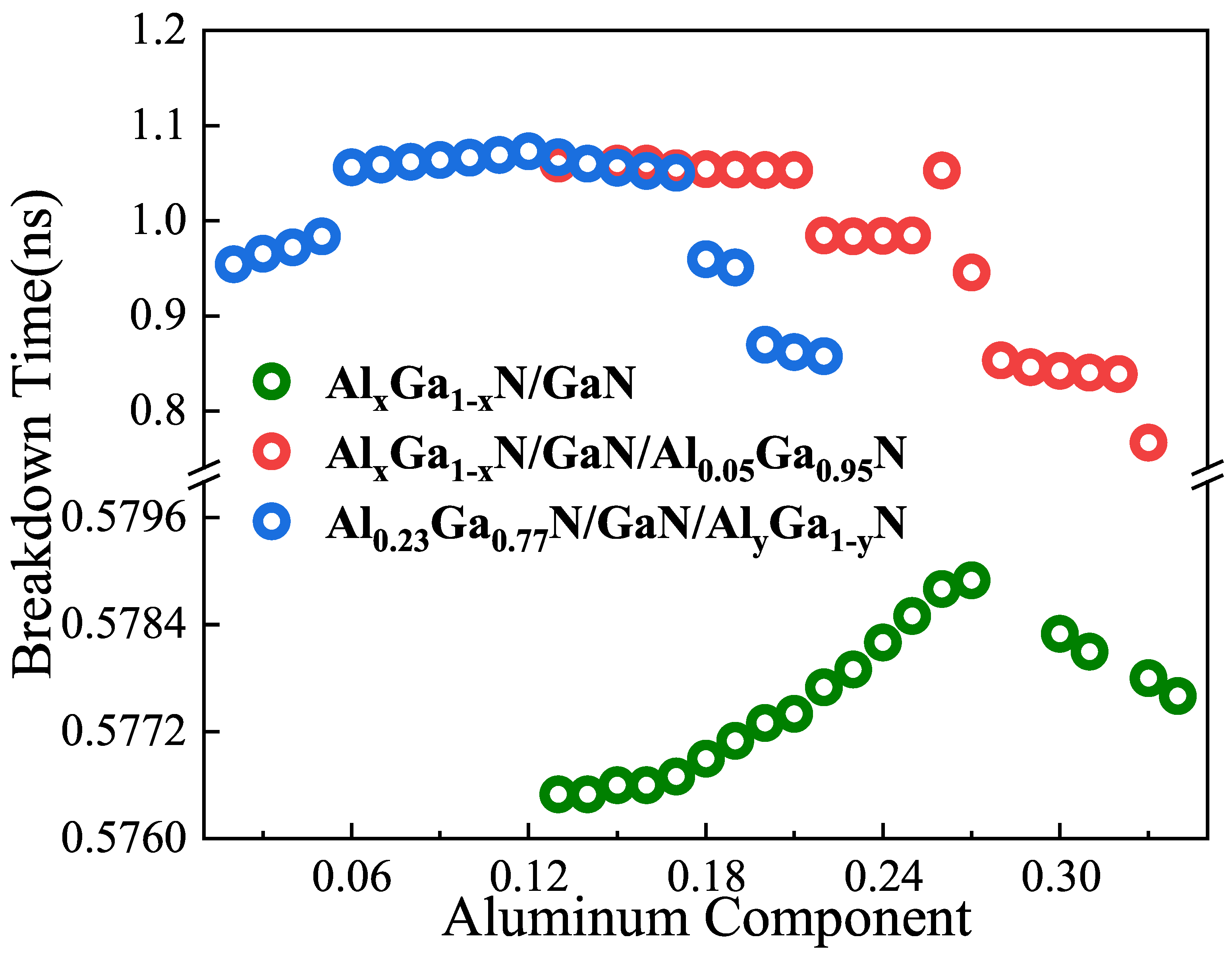
3.2. Effect of Al Composition on Device Breakdown
The energy bands and migration characteristics of the device were altered by the Al component in the AlGaN/GaN structure and hence the breakdown characteristics of the device were affected [25]. In this paper, the effect of the percentage of Al component in single heterojunction AlxGa1−xN/GaN and double heterojunction AlxGa1−xN/GaN/AlyGa1−yN on the breakdown characteristics of the devices was investigated. As can be seen in Figure 6, the Al component in the barrier layer (x between 0.13 and 0.34) and the Al component in the buffer layer (y between 0.02 and 0.22) were separately selected for the study. As the single heterojunction device AlxGa1−xN/GaN (parameter x) and the double heterojunction device Al0.23Ga0.77N/GaN/AlyGa1−yN (parameter y) were increased, the breakdown time also increased and the breakdown resistance of the device improved. This was due to the fact that increasing the Al component increased the bandgap, which resulted in the breakdown characteristics and thermal stability of the device being improved. When the Al component was increased to a certain value, the Al component continued to increase, the barrier width of AlGaN/GaN was reduced, the quantum confinement effect was enhanced, and the high-energy electrons more easily jumped to the conduction band, which in turn reduced the barrier height and decreased the breakdown voltage. The reason for this lies in the alteration of the band structure caused by quantum confinement, resulting in the bending and splitting of energy bands along the confinement axis. Consequently, this alteration had a profound impact on the effective mass of the charge carriers. The confinement of charge carrier motion depicted in Figure 4 further corroborates the influence of quantum confinement on the effective mass. Ultimately, this influence gave rise to a wave function for charge carriers that was discontinuous and non-uniform along the confinement direction. The quantum confinement effect was enhanced due to the domain-limited characteristics of the double heterojunction. This led to the breakdown time of the double heterojunction device AlxGa1−xN/GaN/Al0.02Ga0.98N (x-parameter) being rapidly decreased. Therefore, the breakdown voltage was effectively increased when the Al component was moderately increased. Moreover, compared to the single heterojunction device, the double heterojunction Al component was more sensitive and the breakdown was affected more drastically. Precise control of the Al component doping was achieved by optimizing the doping process parameters, ensuring that the Al component occupied the optimal proportion, and maximizing the breakdown performance of the device. Additionally, the structural parameters of the barrier layer were controlled to ensure a reasonable electric field distribution.

Figure 6.
Effect of the percentage of Al component in AlGaN/GaN on the device breakdown characteristics.
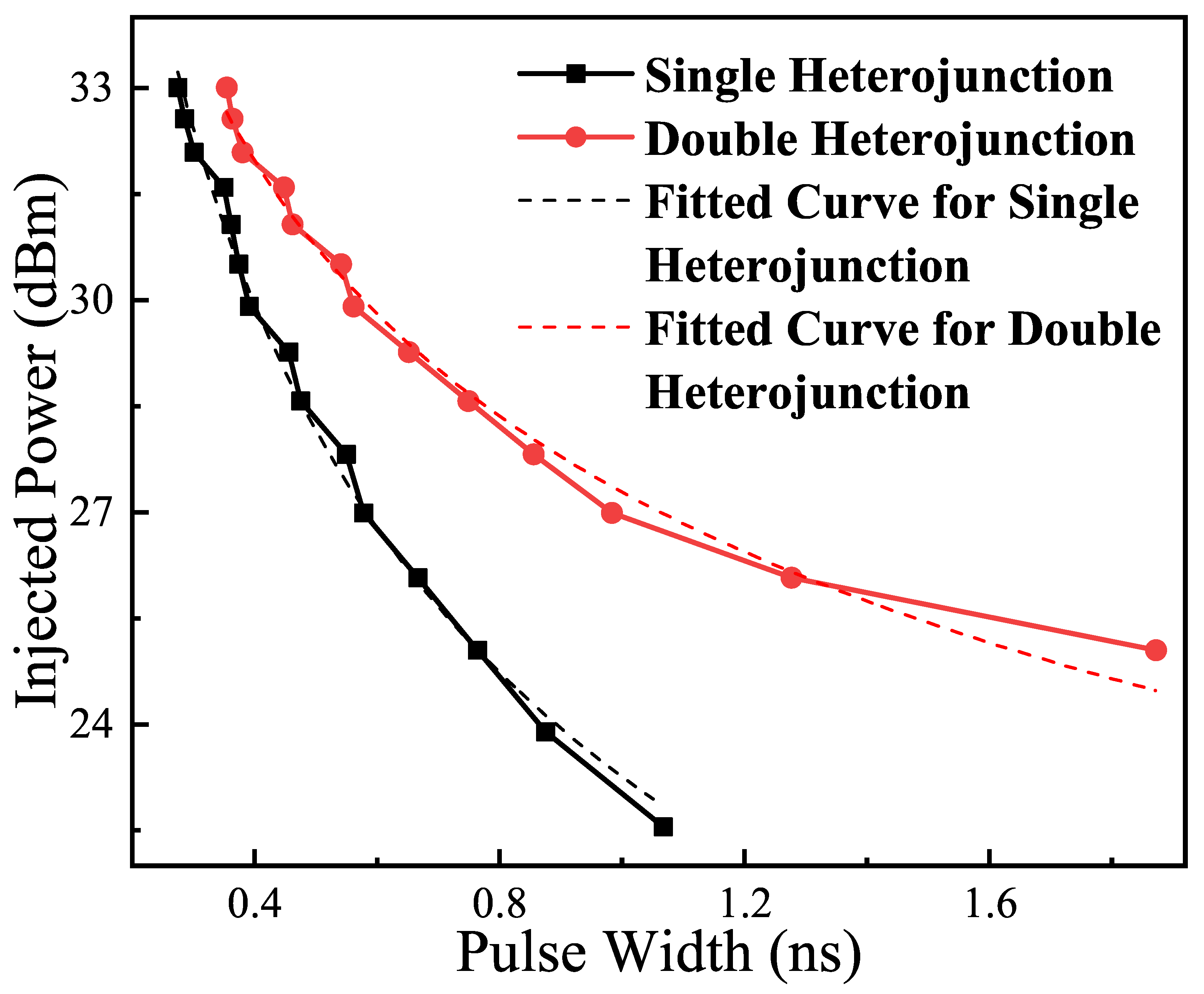
3.3. Effect of Power and Pulse Width on Device Breakdown
Electromagnetic sensitivity (EMS) has been used as a metric for resistance to electromagnetic interference, which has a reliable value impact on the study of electromagnetic damage in HEMT devices. Since frequency and pulse width are inverse to each other, the relationship between the power damage threshold and pulse width was investigated for both single heterojunction and double heterojunction devices to obtain the damage threshold curves in Figure 7. While maintaining a constant pulse width, this study examined the damage effects of different power signals on the device. The traditional research method is to characterize the device as a spherical heat source model [26]; therefore, the damage energy of the device is considered as a constant value. Nevertheless, a new method was used in the literature [27,28,29] to derive a specific value for the variation. The prediction formula for damage was obtained:
where P represents the power value of the gate injection signal; T represents the pulse width (ns); and A is a constant. Data fitting for both device power damage thresholds yielded two nonlinear fitting curves (dashed lines in Figure 7) and a formula for the HPM power damage threshold curve:
where and represent the HPM power damage thresholds of the HEMT devices with single heterojunction and double heterojunction, respectively. and represent the respective correlation coefficients, indicating that the two formulas were fit with very high accuracy, which is in line with conclusions in the literature [24,26]. The formula shows that when the power interacted with the pulse width, the breakdown amplitude of the double heterojunction device was reduced and the stability was increased compared to the single heterojunction HEMT device. The law of power damage threshold and pulse width in GaN HEMT devices is presented in this formulation.
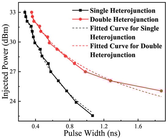
Figure 7.
Power threshold and pulse width were affected on the device.
3.4. Analysis and Discussion
The hardware parameters and data of the device model have been included in this paper as supporting evidence for the quality of the model. The objective of this paper was to present a novel method and theoretical foundation for research.
3.4.1. Discussion on the Quality of the Applied Models
The models provided by Sentaurus-TCAD are primarily based on experimental data, numerical methods, collaborative research and development, academic exchanges, and various other aspects. These foundations jointly ensure the accuracy and reliability of the models, enabling their widespread application in the simulation and design of semiconductor devices. The model used in this paper was a novel model improving upon the mature models in the Sentaurus-TCAD database, aiming to provide a theoretical foundation, while ensuring quality. To further demonstrate the quality of the model, research on the output characteristic curves of the device is included in this paper. However, in reality, the correctness of Figure 2 is the most significant indicator for verifying the correctness of the device.
3.4.2. Discussion on Model Consistency Verification
In Reference [30], a damage experiment of a GaN HEMT caused by high-power microwave pulses demonstrated experimental results of breakdown and damage in the gate region. The experimental device employed in the literature was suitable for the simulation model in this paper. The experimental method was consistent with the simulation method used in this paper. Both device structures were reasonable. Both simulation and experiment confirmed that the region below the gate is one of the most easily damaged parts of the device.
4. Conclusions
Based on the above research and analysis, the following conclusions were drawn. Through a comparative study of single heterojunction and double heterojunction p-GaN HEMT devices, an HPM signal was continuously injected into the gate until device breakdown occurred. An analysis was conducted to investigate the alterations in the internal physical parameters of the devices at the instant of breakdown. The investigation of the results revealed that the peak temperature curve of the device indicated that the device temperature varied according to the posture of the external signal. Analysis of the internal physical characteristics of the device showed that the breakdown occurred at the underside of the gate, demonstrating that the area near the carrier channel under the gate is one of the most vulnerable and susceptible parts of the device to breakdown. Compared to the single heterojunction, the double heterojunction HEMT device suppressed the overflow of 2DEG from the channel to the buffer layer, leading to an improved internal temperature distribution within the device and enhanced injection and transmission efficiency of electrons. The high confinement nature of the double heterojunction reduced leakage current, thereby mitigating the short-channel effect and enhancing the switching characteristics, breakdown characteristics, and stability of the device. This paper further investigated the relationship between Al composition and breakdown, to study the anti-breakdown characteristics of the devices. It was found that the double heterojunction was more sensitive to Al composition, resulting in a stronger impact on breakdown. The electromagnetic sensitivity of the devices was verified by studying the HPM power and pulse width. The HPM power damage threshold curves for single heterojunction and double heterojunction devices were derived as and , respectively. When power and pulse width interacted, the double heterojunction HEMT device exhibited a smaller breakdown amplitude and higher stability compared to the single heterojunction device. The former emerged as an ideal new aviation nanomaterial. Furthermore, when compared to contemporary SiC devices, double heterojunction GaN devices exhibit superior breakdown voltage characteristics and anti-radiation capabilities. In summary, the novel nanodevice proposed in this paper exhibited higher breakdown characteristics and radiation resistance. Furthermore, the mechanism of the temperature increase leading to breakdown within the device was elucidated. This provides an analytical approach for studying the electromagnetic sensitivity of aerospace nanomaterials.
Author Contributions
Conceptualization, Z.M. and D.L.; methodology, Z.M. and D.L.; software, Z.M. and D.L.; validation, Z.M., D.L., S.Y., Z.D. and Z.W.; formal analysis, Z.M. and D.L.; investigation, D.L., S.Y. and Z.D.; resources, Z.M. and D.L.; data curation, D.L.; writing—original draft preparation, D.L.; writing—review and editing, Z.M., D.L., S.Y., Z.D. and Z.W.; visualization, D.L. and Z.D.; supervision, Z.M., D.L., S.Y., Z.D. and Z.W.; project administration, Z.M., D.L. and Z.D.; funding acquisition, Z.M. All authors have read and agreed to the published version of the manuscript.
Funding
This work was supported in part by the Tianjin Science and Technology Bureau Natural Fund Diversified Fund Project Key Project under Grant 21JCZDJC00860, and by the Fundamental Research Funds for the Central Universities (XJ2021003601).
Data Availability Statement
The data that support the findings of this study are available from the corresponding author upon reasonable request.
Conflicts of Interest
The authors declare no conflicts of interest.
References
- Filgueiras, H.; Marques, R.; Augusto, A.R.; Nunes, S.H.; de Faria, H.L.; Cerqueira, S.A. HIRF Broadband Full-Wave Virtual Testing and Experimental Validation. IEEE Electromagn. Compat. Mag. 2021, 10, 39–46. [Google Scholar] [CrossRef]
- Kadem, K.; Benyoubi, F.; Bensetti, M.; Bihan, Y.L.; Labouré, E.; Debbou, M. An Efficient Method for Dimensioning Magnetic Shielding for an Induction Electric Vehicle Charging System. Prog. Electromagn. Res. 2021, 170, 153–167. [Google Scholar] [CrossRef]
- Wu, Z.; Liu, P.; Deng, B.; Tian, T.; Zha, S.; Ni, X. An Ultrabroadband Energy Selective Surface with Nonreciprocal Performance for HIRF Protection. IEEE Trans. Electromagn. Compat. 2023, 65, 1202–1210. [Google Scholar] [CrossRef]
- Weinberg, G.V. Quantification of combat team survivability with high power rf directed energy weapons. Prog. Electromagn. Res. M 2021, 102, 1–11. [Google Scholar] [CrossRef]
- Marjanovic Cermak, A.M.; Pavicic, I.; Trosic, I. Oxidative stress response in SH-SY5Y cells exposed to short-term 1800 MHz radiofrequency radiation. J. Environ. Sci. Health Part A Toxic/Hazardous Subst. Environ. Eng. 2018, 53, 132–138. [Google Scholar]
- Ying, K.; Yu, X.; Shen, J.; Zhang, S.; Guo, Y. Intelligent Microwave Staring Correlated Imaging. Prog. Electromagn. Res. 2023, 176, 109–128. [Google Scholar] [CrossRef]
- Arpia, A.A.; Chen, W.H.; Lam, S.S.; Rousset, P.; Luna, M.D.G.D. Sustainable biofuel and bioenergy production from biomass waste residues using microwave-assisted heating: A comprehensive review. Chem. Eng. J. 2021, 403, 126233. [Google Scholar] [CrossRef]
- Xie, Y.; Li, Z.; Tang, J.; Li, P.; Chen, W.; Liu, P.; Li, L.; Zheng, Z. Microwave-assisted foaming and sintering to prepare lightweight high-strength polystyrene/carbon nanotube composite foams with an ultralow percolation threshold. J. Mater. Chem. C 2021, 9, 9702–9711. [Google Scholar] [CrossRef]
- Jafari, A.; Nikoo, M.S.; Perera, N.; Yildirim, H.K.; Karakaya, F.; Soleimanzadeh, R.; Matioli, E. Comparison of Wide-Band-Gap Technologies for Soft-Switching Losses at High Frequencies. IEEE Trans. Power Electron. 2020, 35, 12595–12600. [Google Scholar] [CrossRef]
- Wei, X.; Shen, W.; Zhou, X.; Tang, W.; Ma, Y.; Chen, T.; Wang, D.; Fu, H.; Zhang, X.; Lin, W.; et al. 2.69 kV/2.11 mΩ·cm and Low Leakage p-GaN Stripe Array Gated Hybrid Anode Diodes with Low Turn-on Voltage. IEEE Electron Device Lett. 2023, 44, 13–16. [Google Scholar] [CrossRef]
- Wang, Y.; Sun, H.; Zhao, Q.; Mao, Y.; Hou, Q. Study on Capability Verification Test of Electromagnetic Pulse Protection for Aircraft. In Proceedings of the 2022 Asia-Pacific International Symposium on Electromagnetic Compatibility (APEMC), Beijing, China, 8–11 May 2022; pp. 391–393. [Google Scholar] [CrossRef]
- Xiao, J.; Song, Z.; Wang, J.; Wang, L. Simulation Analysis of Electromagnetic Shielding of Electronic Device Chassis. In Proceedings of the 2019 12th International Workshop on the Electromagnetic Compatibility of Integrated Circuits (EMC Compo), Hangzhou, China, 21–23 October 2019; pp. 91–93. [Google Scholar] [CrossRef]
- Tallarico, A.N.; Stoffels, S.; Posthuma, N.; Decoutere, S.; Sangiorgi, E.; Fiegna, C. Threshold Voltage Instability in GaN HEMTs with p-Type Gate: Mg Doping Compensation. IEEE Electron Device Lett. 2019, 40, 518–521. [Google Scholar] [CrossRef]
- Hou, R.; Shen, Y.; Zhao, H.; Hu, H.; Lu, J.; Long, T. Power Loss Characterization and Modeling for GaN-Based Hard-Switching Half-Bridges Considering Dynamic on-State Resistance. IEEE Trans. Transp. Electrif. 2020, 6, 540–553. [Google Scholar] [CrossRef]
- Meguro, T.; Takeyama, A.; Ohshima, T.; Tanaka, Y.; Kuroki, S.I. Hybrid Pixels with Si Photodiode and 4H-SiC MOSFETs Using Direct Heterogeneous Bonding Toward Radiation Hardened CMOS Image Sensors. IEEE Electron Device Lett. 2022, 43, 1713–1716. [Google Scholar] [CrossRef]
- Wu, H. Research on the Characteristics of GaN DHEMT. Master’s Thesis, Xi’an University of Technology, Xi’an, China, 2024. [Google Scholar]
- Moon, J.S.; Grabar, B.; Wong, J.; Chuong, D.; Arkun, E.; Morales, D.V.; Chen, P.; Malek, C.; Fanning, D.; Venkatesan, N.; et al. Power Scaling of Graded-Channel GaN HEMTs with Mini-Field-Plate T-gate and 156 GHz fT. IEEE Electron Device Lett. 2021, 42, 796–799. [Google Scholar] [CrossRef]
- Ahmeda, K.; Ubochi, B.; Alqaysi, M.; Al-Khalidi, A.; Kalna, K. The role of SiN/GaN cap interface charge and GaN cap layer to achieve enhancement mode GaN MIS-HEMT operation. Microelectron. Reliab. 2020, 115, 113965. [Google Scholar] [CrossRef]
- Zhang, L.; Zheng, Z.; Yang, S.; Song, W.; Chen, K.J. p-GaN Gate HEMT with Surface Reinforcement for Enhanced Gate Reliability. IEEE Electron Device Lett. 2020, 42, 22–25. [Google Scholar] [CrossRef]
- Song, W.; Zheng, Z.; Chen, T.; Wei, J.; Yuan, L.; Chen, K.J. RF Linearity Enhancement of GaN-on-Si HEMTs with a Closely Coupled Double-Channel Structure. IEEE Electron Device Lett. 2021, 42, 1116–1119. [Google Scholar] [CrossRef]
- Kamath, A.; Patil, T.; Adari, R.; Bhattacharya, I.; Ganguly, S.; Aldhaheri, R.W.; Hussain, M.A.; Saha, D. Double-Channel AlGaN/GaN High Electron Mobility Transistor with Back Barriers. IEEE Electron Device Lett. 2012, 33, 1690–1692. [Google Scholar] [CrossRef]
- Yang, L.; Changchun, C.; Xinhai, Y.; Qingyang, F.; Yintang, Y.; Xiaowen, X.; Shengbei, L. Damage effects and mechanism of the GaN high electron mobility transistor caused by high electromagnetic pulse. Acta Phys. Sin. 2016, 65, 038402. [Google Scholar] [CrossRef]
- Synopsys. SentaurusTM Device User Guide; Synopsys: Tokyo, Japan, 2018. [Google Scholar]
- Yu, X.; Ma, Z.; Chai, C.; Shi, C.; Wang, P. Nonlinear and Permanent Degradation of GaAs-Based Low-Noise Amplifier Under Electromagnetic Pulse Injection. IEEE Trans. Electromagn. Compat. 2020, 62, 101–107. [Google Scholar] [CrossRef]
- Meneghesso, G.; Meneghini, M.; Zanoni, E. Breakdown mechanisms in AlGaN/GaN HEMTs: An overview. Jpn. J. Appl. Phys. 2014, 53, 100211. [Google Scholar] [CrossRef]
- Changchun, C.; Xiaowen, X.; Xingrong, R.; Yintang, Y.; Zhenyang, M. The damage effect and mechanism of the bipolar transistor induced by the intense electromagnetic pulse. Acta Phys. Sin. 2010, 59, 8118–8124. [Google Scholar] [CrossRef]
- Xiaowen, X.; Changchun, C.; Xingrong, R.; Yintang, Y.; Bing, Z. EMP injection damage effects of a bipolar transistor and its relationship between the injecting voltage and energy. J. Semicond. 2010, 31, 44005. [Google Scholar] [CrossRef]
- Brown, W.D. Semiconductor Device Degradation by High Amplitude Current Pulses. IEEE Trans. Nucl. Sci. 1972, 19, 68–75. [Google Scholar] [CrossRef]
- Wunsch, D.C.; Bell, R.R. Determination of Threshold Failure Levels of Semiconductor Diodes and Transistors Due to Pulse Voltages. IEEE Trans. Nucl. Sci. 1968, 15, 244–259. [Google Scholar] [CrossRef]
- Zhou, L.; San, Z.W.; Hua, Y.J.; Lin, L.; Zhang, S.; Zhao, Z.G.; Zhou, H.J.; Yin, W.Y. Investigation on Failure Mechanisms of GaN HEMT Caused by High-Power Microwave (HPM) Pulses. IEEE Trans. Electromagn. Compat. 2017, 59, 902–909. [Google Scholar] [CrossRef]
Disclaimer/Publisher’s Note: The statements, opinions and data contained in all publications are solely those of the individual author(s) and contributor(s) and not of MDPI and/or the editor(s). MDPI and/or the editor(s) disclaim responsibility for any injury to people or property resulting from any ideas, methods, instructions or products referred to in the content. |
© 2024 by the authors. Licensee MDPI, Basel, Switzerland. This article is an open access article distributed under the terms and conditions of the Creative Commons Attribution (CC BY) license (https://creativecommons.org/licenses/by/4.0/).