
Nano-Level Additive Manufacturing: Condensed Review of Processes, Materials, and Industrial Applications

 , ,
, , 
Abstract
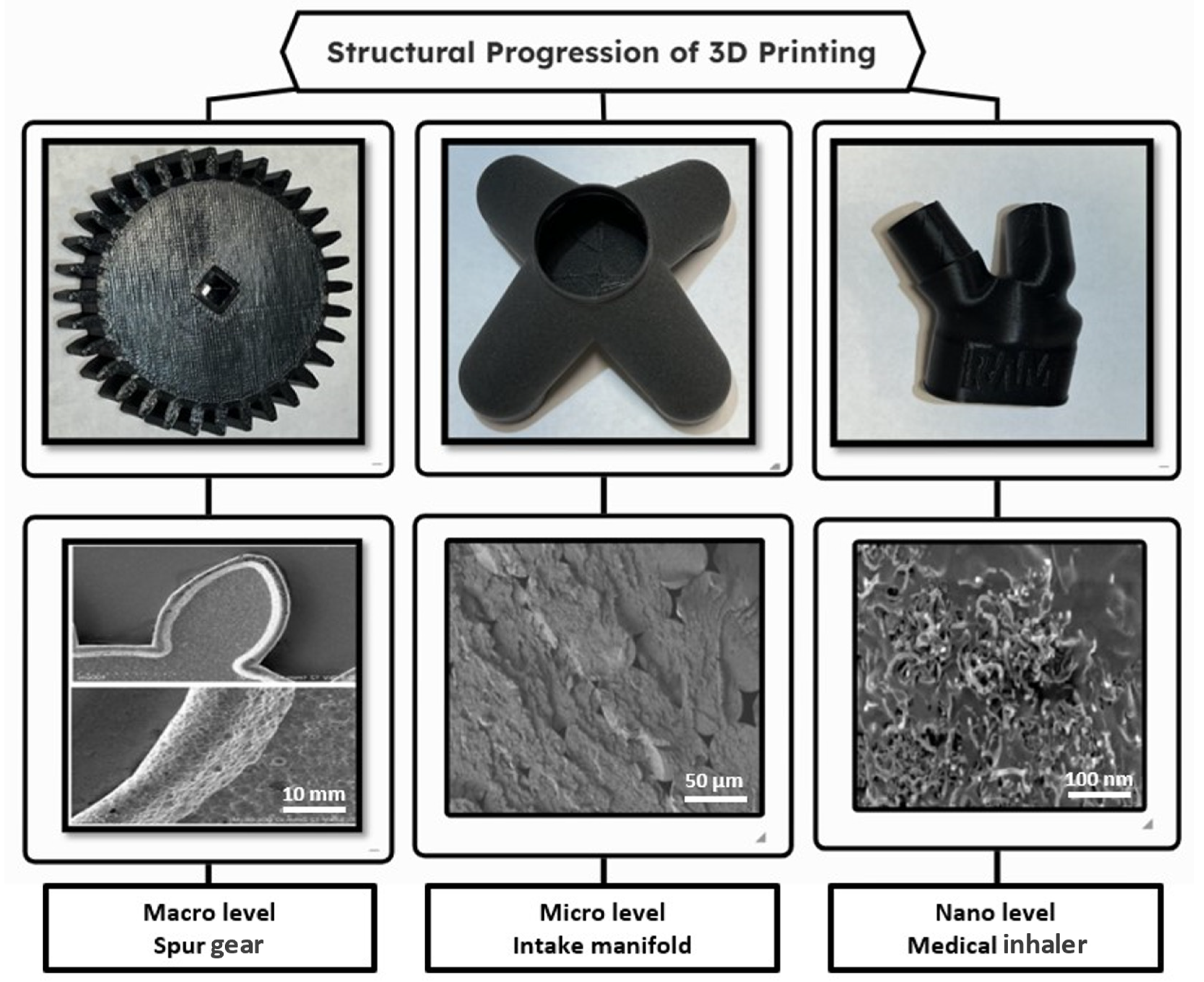
:1. Introduction
2. Nano 3D Printing Processes
2.1. Traditional Processes
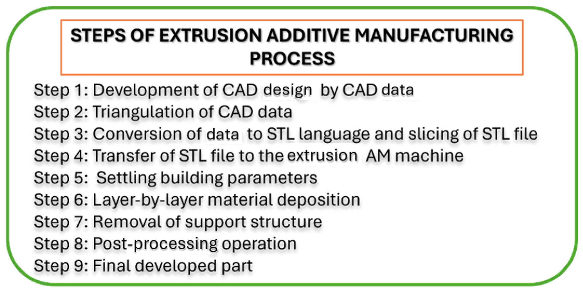
2.1.1. Material Extrusion
2.1.2. VAT Photopolymerization
2.1.3. Inkjet Printing
2.2. Non-Traditional Processes
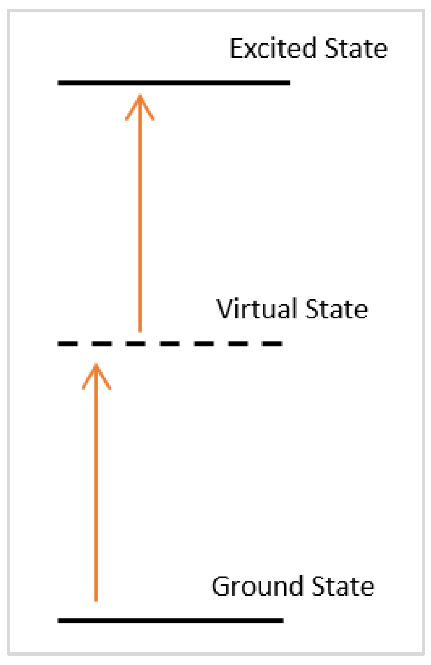
2.2.1. Two-Photon Polymerization
2.2.2. Laser-Induced Forward Transfer
3. Materials
3.1. Types of Nanomaterials
3.1.1. Organic Nanoparticles
3.1.2. Inorganic Nanoparticles
3.2. Dimensions of Nanomaterials
3.2.1. Zero-Dimensional (0D)
3.2.2. One-Dimensional (1D)
3.2.3. Two-Dimensional (2D)
3.2.4. Three-Dimensional (3D)
3.3. Geometric Shapes of Nanomaterials
3.3.1. Spherical Nanomaterials
3.3.2. Cylindrical Nanomaterials
3.3.3. Platelet or Disc-Shaped Nanomaterials
3.3.4. Bricklike or Cuboidal Nanomaterials
4. Industrial Perspective
4.1. UpNano GmbH
4.2. Nanoss GmbH
4.3. Nanoscribe
4.4. Nano3Dprint
4.5. Nano Dimension
5. Future Perspectives and Trends
6. Conclusions
Author Contributions
Funding
Data Availability Statement
Acknowledgments
Conflicts of Interest
Abbreviations
| AM | Additive manufacturing |
| 3DP | 3D printing |
| CAD | Computer-aided design |
| 3D | Three-dimensional |
| R&D | Research and development |
| MEX | Material Extrusion |
| FFF | Fused Filament Fabrication |
| FDM | Fused Deposition Modeling |
| VPP | VAT Photopolymerization |
| PBF | Powder Bed Fusion |
| NM | Nano material |
| MJ | Material Jetting |
| BJ | Binder Jetting |
| SL | Sheet Lamination |
| DED | Directed energy deposition |
| SLS | Selective Laser Sintering |
| WAAM | Wire-arc additive manufacturing |
| DIW | Direct ink writing |
| BCPs | Block copolymers |
| PS | Poly(styrene) |
| SEM | Scanning Electron Microscope |
| TPP | Two-photon polymerization |
| TPA | Two-photon absorption |
| CNT | Carbon nanotubes |
| DLW | Direct laser writing |
| LIFT | Laser-Induced Forward Transfer |
| FWHM | Full Width at Half-Maximum |
| SWCNTs | Single-walled carbon nanotubes |
| MWCNTs | Multi-walled carbon nanotubes |
| HA | Hydroxyapatite |
| SLA | Stereolithography |
| EC | European Commission |
| e-AM | Electrochemical AM |
References
- Zhang, Z.; Femi-Oyetoro, J.; Fidan, I.; Ismail, M.; Allen, M. Prediction of Dimensional Changes of Low-Cost Metal Material Extrusion Fabricated Parts Using Machine Learning Techniques. Metals 2021, 11, 690. [Google Scholar] [CrossRef]
- Zhang, Z.; Fidan, I.; Allen, M. Detection of Material Extrusion In-Process Failures via Deep Learning. Inventions 2020, 5, 25. [Google Scholar] [CrossRef]
- Wohlers, T.; Gornet, T.; Mostow, N.; Campbell, I.; Diegel, O.; Kowen, J.; Huff, R.; Stucker, B.; Fidan, I.; Doukas, A.; et al. History of Additive Manufacturing. SSRN Electron. J. 2016, 1–38. [Google Scholar] [CrossRef]
- Blanco, I. The Use of Composite Materials in 3D Printing. J. Compos. Sci. 2020, 4, 42. [Google Scholar] [CrossRef]
- ISO/ASTM 52900:2021; Additive Manufacturing—General Principles—Fundamentals and Vocabulary. ISO: Geneva, Switzerland, 2021. Available online: https://www.iso.org/standard/74514.html#lifecycle (accessed on 23 May 2024).
- Zhang, Z.; Fidan, I. Machine Learning-Based Void Percentage Analysis of Components Fabricated with the Low-Cost Metal Material Extrusion Process. Materials 2022, 15, 4292. [Google Scholar] [CrossRef]
- Attaran, M. The Rise of 3-D Printing: The Advantages of Additive Manufacturing over Traditional Manufacturing. Bus. Horiz. 2017, 60, 677–688. [Google Scholar] [CrossRef]
- Huseynov, O.; Patterson, A.E.; Ali, M.A.; Gupta, A.; Gudavasov, S.; Mahmudov, M.; Hasanov, S.; Fidan, I. Critical Review on Short Fiber-Reinforced Composite Materials Manufactured by Material Extrusion: From Thermal Perspective. Progress Addit. Manuf. 2024, 1–26. [Google Scholar] [CrossRef]
- Outrequin, T.C.R.; Gamonpilas, C.; Siriwatwechakul, W.; Sreearunothai, P. Extrusion-Based 3D Printing of Food Biopolymers: A Highlight on the Important Rheological Parameters to Reach Printability. J. Food Eng. 2023, 342, 111371. [Google Scholar] [CrossRef]
- Serrano, D.R.; Kara, A.; Yuste, I.; Luciano, F.C.; Ongoren, B.; Anaya, B.J.; Molina, G.; Diez, L.; Ramirez, B.I.; Ramirez, I.O.; et al. 3D Printing Technologies in Personalized Medicine, Nanomedicines, and Biopharmaceuticals. Pharmaceutics 2023, 15, 313. [Google Scholar] [CrossRef]
- Mishra, P.K.; Jagadesh, T. Applications and Challenges of 3D Printed Polymer Composites in the Emerging Domain of Automotive and Aerospace: A Converged Review. J. Inst. Eng. Ser. D 2023, 104, 849–866. [Google Scholar] [CrossRef]
- Elsafi, M.; El-Nahal, M.A.; Sayyed, M.I.; Saleh, I.H.; Abbas, M.I. Novel 3-D Printed Radiation Shielding Materials Embedded with Bulk and Nanoparticles of Bismuth. Sci. Rep. 2022, 12, 12467. [Google Scholar] [CrossRef] [PubMed]
- Hunde, B.R.; Woldeyohannes, A.D. 3D Printing and Solar Cell Fabrication Methods: A Review of Challenges, Opportunities, and Future Prospects. Results Opt. 2023, 11, 100385. [Google Scholar] [CrossRef]
- Mohammed, A.A.; Algahtani, M.S.; Ahmad, M.Z.; Ahmad, J.; Kotta, S. 3D Printing in Medicine: Technology Overview and Drug Delivery Applications. Ann. 3D Print. Med. 2021, 4, 100037. [Google Scholar] [CrossRef]
- Kalkal, A.; Kumar, S.; Kumar, P.; Pradhan, R.; Willander, M.; Packirisamy, G.; Kumar, S.; Malhotra, B.D. Recent Advances in 3D Printing Technologies for Wearable (Bio)Sensors. Addit. Manuf. 2021, 46, 102088. [Google Scholar] [CrossRef]
- Sikora, P.; Chougan, M.; Cuevas, K.; Liebscher, M.; Mechtcherine, V.; Ghaffar, S.H.; Liard, M.; Lootens, D.; Krivenko, P.; Sanytsky, M.; et al. The Effects of Nano- and Micro-Sized Additives on 3D Printable Cementitious and Alkali-Activated Composites: A Review. Appl. Nanosci. 2021, 12, 805–823. [Google Scholar] [CrossRef]
- Meng, Y.; Cao, J.; Chen, Y.; Yu, Y.; Ye, L. 3D Printing of a Poly(Vinyl Alcohol)-Based Nano-Composite Hydrogel as an Artificial Cartilage Replacement and the Improvement Mechanism of Printing Accuracy. J. Mater. Chem. B 2020, 8, 677–690. [Google Scholar] [CrossRef] [PubMed]
- Greer, A.I.M.; Barbour, E.; Cutiongco, M.F.; Stormonth-Darling, J.M.; Convery, N.; Alsaigh, R.E.; Lavery, M.P.J.; Gadegaard, N. Large Volume Nanoscale 3D Printing: Nano-3DP. Appl. Mater. Today 2020, 21, 100782. [Google Scholar] [CrossRef]
- Rahman, M.; Islam, K.S.; Dip, T.M.; Chowdhury, M.F.M.; Debnath, S.R.; Hasan, S.M.M.; Sakib, M.S.; Saha, T.; Padhye, R.; Houshyar, S. A Review on Nanomaterial-Based Additive Manufacturing: Dynamics in Properties, Prospects, and Challenges. Progress Addit. Manuf. 2023, 9, 1197–1224. [Google Scholar] [CrossRef]
- Abouzeid, R.E.; Khiari, R.; Salama, A.; Diab, M.; Beneventi, D.; Dufresne, A. In Situ Mineralization of Nano-Hydroxyapatite on Bifunctional Cellulose Nanofiber/Polyvinyl Alcohol/Sodium Alginate Hydrogel Using 3D Printing. Int. J. Biol. Macromol. 2020, 160, 538–547. [Google Scholar] [CrossRef]
- Ren, B.; Wan, Y.; Liu, C.; Wang, H.; Yu, M.; Zhang, X.; Huang, Y. Improved Osseointegration of 3D Printed Ti-6Al-4V Implant with a Hierarchical Micro/Nano Surface Topography: An in Vitro and in Vivo Study. Mater. Sci. Eng. C 2021, 118, 111505. [Google Scholar] [CrossRef]
- Chougan, M.; Hamidreza Ghaffar, S.; Jahanzat, M.; Albar, A.; Mujaddedi, N.; Swash, R. The Influence of Nano-Additives in Strengthening Mechanical Performance of 3D Printed Multi-Binder Geopolymer Composites. Constr. Build. Mater. 2020, 250, 118928. [Google Scholar] [CrossRef]
- Sezer, H.K.; Eren, O. FDM 3D Printing of MWCNT Re-Inforced ABS Nano-Composite Parts with Enhanced Mechanical and Electrical Properties. J. Manuf. Process 2019, 37, 339–347. [Google Scholar] [CrossRef]
- Yan, S.; Huang, Y.; Zhao, D.; Niu, F.; Ma, G.; Wu, D. 3D Printing of Nano-Scale Al2O3-ZrO2 Eutectic Ceramic: Principle Analysis and Process Optimization of Pores. Addit. Manuf. 2019, 28, 120–126. [Google Scholar] [CrossRef]
- Li, J.; Li, K.; Du, Y.; Tang, X.; Liu, C.; Cao, S.; Zhao, B.; Huang, H.; Zhao, H.; Kong, W.; et al. Dual-Nozzle 3D Printed Nano-Hydroxyapatite Scaffold Loaded with Vancomycin Sustained-Release Microspheres for Enhancing Bone Regeneration. Int. J. Nanomed. 2023, 18, 307–322. [Google Scholar] [CrossRef] [PubMed]
- Cheng, L.; Shoma Suresh, K.; He, H.; Rajput, R.S.; Feng, Q.; Ramesh, S.; Wang, Y.; Krishnan, S.; Ostrovidov, S.; Camci-Unal, G.; et al. 3d Printing of Micro-and Nanoscale Bone Substitutes: A Review on Technical and Translational Perspectives. Int. J. Nanomed. 2021, 16, 4289–4319. [Google Scholar] [CrossRef] [PubMed]
- Manzoor, F.; Golbang, A.; Jindal, S.; Dixon, D.; McIlhagger, A.; Harkin-Jones, E.; Crawford, D.; Mancuso, E. 3D Printed PEEK/HA Composites for Bone Tissue Engineering Applications: Effect of Material Formulation on Mechanical Performance and Bioactive Potential. J. Mech. Behav. Biomed. Mater. 2021, 121, 104601. [Google Scholar] [CrossRef] [PubMed]
- Montalbano, G.; Molino, G.; Fiorilli, S.; Vitale-Brovarone, C. Synthesis and Incorporation of Rod-like Nano-Hydroxyapatite into Type I Collagen Matrix: A Hybrid Formulation for 3D Printing of Bone Scaffolds. J. Eur. Ceram. Soc. 2020, 40, 3689–3697. [Google Scholar] [CrossRef]
- Hassan, M.; Dave, K.; Chandrawati, R.; Dehghani, F.; Gomes, V.G. 3D Printing of Biopolymer Nanocomposites for Tissue Engineering: Nanomaterials, Processing and Structure-Function Relation. Eur. Polym. J. 2019, 121, 109340. [Google Scholar] [CrossRef]
- Yeo, M.; Kim, G.H. Micro/Nano-Hierarchical Scaffold Fabricated Using a Cell Electrospinning/3D Printing Process for Co-Culturing Myoblasts and HUVECs to Induce Myoblast Alignment and Differentiation. Acta Biomater. 2020, 107, 102–114. [Google Scholar] [CrossRef]
- Muldoon, K.; Song, Y.; Ahmad, Z.; Chen, X.; Chang, M.W. High Precision 3D Printing for Micro to Nano Scale Biomedical and Electronic Devices. Micromachines 2022, 13, 642. [Google Scholar] [CrossRef]
- Cao, Q.; Shin, M.; Lavrik, N.V.; Venton, B.J. 3D-Printed Carbon Nanoelectrodes for in Vivo Neurotransmitter Sensing. Nano Lett. 2020, 20, 6831–6836. [Google Scholar] [CrossRef] [PubMed]
- Ulrich, S.; Wang, X.; Rottmar, M.; Rossi, R.M.; Nelson, B.J.; Bruns, N.; Müller, R.; Maniura-Weber, K.; Qin, X.H.; Boesel, L.F. Nano-3D-Printed Photochromic Micro-Objects. Small 2021, 17, 2101337. [Google Scholar] [CrossRef] [PubMed]
- Wei, Y.; Shi, C.; Zhang, Y.; Liu, C.; Tang, Y.; Ren, P.; Wang, C.; Zhang, Y.U.; Liu, Z. Temperature-Compensated Fiber-Optic SPR Microfluidic Sensor Based on Micro-Nano 3D Printing. Opt. Express 2023, 31, 38179–38190. [Google Scholar] [CrossRef] [PubMed]
- Beliatis, M.J.; Lindberg, J.R.; Ostergaard, B.R.; Pokorniecki, D.; Gross, A.; Presser, M. Development of a Robotic 3D Printing Polymer Extruder with Laser and FTIR for Nano-Manufacturing and Characterization. In Proceedings of the IEEE Conference on Nanotechnology 2022, Palma de Mallorca, Spain, 4–8 July 2022; pp. 100–103. [Google Scholar] [CrossRef]
- Gupta, A.; Hasanov, S.; Alifui-Segbaya, F.; Fidan, I. Composites (Fiber-Reinforced Plastic Matrix Composites). In Springer Handbook of Additive Manufacturing; Springer Handbooks; Springer: Cham, Swtizerland, 2023; Part F1592; pp. 627–637. [Google Scholar] [CrossRef]
- Alifui-Segbaya, F.; Ituarte, I.F.; Hasanov, S.; Gupta, A.; Fidan, I. Opportunities and Limitations of Additive Manufacturing. In Springer Handbook of Additive Manufacturing; Springer Handbooks; Springer: Berlin/Heidelberg, Germany, 2023; Part F1592; pp. 125–143. [Google Scholar] [CrossRef]
- Altıparmak, S.C.; Yardley, V.A.; Shi, Z.; Lin, J. Extrusion-Based Additive Manufacturing Technologies: State of the Art and Future Perspectives. J. Manuf. Process 2022, 83, 607–636. [Google Scholar] [CrossRef]
- Bouzaglou, O.; Golan, O.; Lachman, N. Process Design and Parameters Interaction in Material Extrusion 3D Printing: A Review. Polymers 2023, 15, 2280. [Google Scholar] [CrossRef] [PubMed]
- Mohd Pu’ad, N.A.S.; Abdul Haq, R.H.; Mohd Noh, H.; Abdullah, H.Z.; Idris, M.I.; Lee, T.C. Review on the Fabrication of Fused Deposition Modelling (FDM) Composite Filament for Biomedical Applications. Mater. Today Proc. 2020, 29, 228–232. [Google Scholar] [CrossRef]
- Tümer, E.H.; Erbil, H.Y. Extrusion-Based 3D Printing Applications of PLA Composites: A Review. Coatings 2021, 11, 390. [Google Scholar] [CrossRef]
- Terry, S.; Lu, H.; Fidan, I.; Zhang, Y.; Tantawi, K.; Guo, T.; Asiabanpour, B. The Influence of Smart Manufacturing towards Energy Conservation: A Review. Technologies 2020, 8, 31. [Google Scholar] [CrossRef]
- Layani, M.; Wang, X.; Magdassi, S. Novel Materials for 3D Printing by Photopolymerization. Adv. Mater. 2018, 30, 1706344. [Google Scholar] [CrossRef] [PubMed]
- Naik, D.L.; Kiran, R. On Anisotropy, Strain Rate and Size Effects in Vat Photopolymerization Based Specimens. Addit. Manuf. 2018, 23, 181–196. [Google Scholar] [CrossRef]
- Batista, M.; Mora-Jimenez, J.; Salguero, J.; Vazquez-Martinez, J.M.; Batista, M.; Mora-Jimenez, J.; Salguero, J.; Manuel Vazquez-Martinez, J. Assessment of the Development Performance of Additive Manufacturing VPP Parts Using Digital Light Processing (DLP) and Liquid Crystal Display (LCD) Technologies. Appl. Sci. 2024, 14, 3607. [Google Scholar] [CrossRef]
- Medellin, A.; Du, W.; Miao, G.; Zou, J.; Pei, Z.; Ma, C. Vat Photopolymerization 3d Printing of Nanocomposites: A Literature Review. J. Micro Nanomanuf. 2019, 7, 031006. [Google Scholar] [CrossRef]
- Li, Y.; Wang, W.; Wu, F.; Kankala, R.K. Vat Polymerization-Based 3D Printing of Nanocomposites: A Mini Review. Front. Mater. 2023, 9, 1118943. [Google Scholar] [CrossRef]
- Shirazi, S.F.S.; Gharehkhani, S.; Mehrali, M.; Yarmand, H.; Metselaar, H.S.C.; Adib Kadri, N.; Osman, N.A.A. A Review on Powder-Based Additive Manufacturing for Tissue Engineering: Selective Laser Sintering and Inkjet 3D Printing. Sci. Technol. Adv. Mater. 2015, 16, 033502. [Google Scholar] [CrossRef] [PubMed]
- Ricci, S.; Buonomo, M.; Casalini, S.; Bonacchi, S.; Meneghetti, M.; Litti, L. High Performance Multi-Purpose Nanostructured Thin Films by Inkjet Printing: Au Micro-Electrodes and SERS Substrates. Nanoscale Adv. 2023, 5, 1970–1977. [Google Scholar] [CrossRef] [PubMed]
- Lim, S. Inkjet Printability of Electronic Materials Important to the Manufacture of Fully Printed OTFTS; Western Michigan University ProQuest Dissertations Publishing: Kalamazoo, MI, USA, 2012; p. 3531907. [Google Scholar]
- Calvert, P. Inkjet Printing for Materials and Devices. Chem. Mater. 2001, 13, 3299–3305. [Google Scholar] [CrossRef]
- Zhang, H.; Massingill, J.L.; Woo, J.T.K. Low VOC, Low Viscosity UV Cationic Radiation-Cured Ink-Jet Ink System. J. Coat. Technol. 2000, 72, 45–52. [Google Scholar] [CrossRef]
- Karkun, M.S.; Dharmalingam, S. 3D Printing Technology in Aerospace Industry—A Review. Int. J. Aviat. Aeronaut. Aerosp. 2022, 9, 4. [Google Scholar] [CrossRef]
- El-Sayegh, S.; Romdhane, L.; Manjikian, S. A Critical Review of 3D Printing in Construction: Benefits, Challenges, and Risks. Arch. Civ. Mech. Eng. 2020, 20, 34. [Google Scholar] [CrossRef]
- Nadagouda, M.N.; Rastogi, V.; Ginn, M. A Review on 3D Printing Techniques for Medical Applications. Curr. Opin. Chem. Eng. 2020, 28, 152–157. [Google Scholar] [CrossRef]
- Bunea, A.I.; Szczotka, N.; Navne, J.; Taboryski, R. Single-Step Fabrication of Superhydrophobic Surfaces by Two-Photon Polymerization Micro 3D Printing. Micro Nano Eng. 2023, 19, 100192. [Google Scholar] [CrossRef]
- Göppert-Mayer, M. Über Elementarakte Mit Zwei Quantensprüngen. Ann. Phys. 1931, 401, 273–294. [Google Scholar] [CrossRef]
- Faraji Rad, Z.; Prewett, P.D.; Davies, G.J. High-Resolution Two-Photon Polymerization: The Most Versatile Technique for the Fabrication of Microneedle Arrays. Microsyst. Nanoeng. 2021, 7, 71. [Google Scholar] [CrossRef] [PubMed]
- Paz, V.F.; Emons, M.; Obata, K.; Ovsianikov, A.; Peterhänsel, S.; Frenner, K.; Reinhardt, C.; Chichkov, B.; Morgner, U.; Osten, W. Development of Functional Sub-100 Nm Structures with 3D Two-Photon Polymerization Technique and Optical Methods for Characterization. J. Laser Appl. 2012, 24, 042004. [Google Scholar] [CrossRef]
- Tkachenko, N.V. Optical Spectroscopy: Methods and Instrumentations; Elsevier: Amsterdam, The Netherlands, 2006. [Google Scholar]
- O’Halloran, S.; Pandit, A.; Heise, A.; Kellett, A. Two-Photon Polymerization: Fundamentals, Materials, and Chemical Modification Strategies. Adv. Sci. 2023, 10, 2204072. [Google Scholar] [CrossRef] [PubMed]
- Jing, X.; Fu, H.; Yu, B.; Sun, M.; Wang, L. Two-Photon Polymerization for 3D Biomedical Scaffolds: Overview and Updates. Front. Bioeng. Biotechnol. 2022, 10, 994355. [Google Scholar] [CrossRef] [PubMed]
- Marschner, D.E.; Pagliano, S.; Huang, P.H.; Niklaus, F. A Methodology for Two-Photon Polymerization Micro 3D Printing of Objects with Long Overhanging Structures. Addit. Manuf. 2023, 66, 103474. [Google Scholar] [CrossRef]
- Bohandy, J.; Kim, B.F.; Adrian, F.J. Metal Deposition from a Supported Metal Film Using an Excimer Laser. J. Appl. Phys. 1986, 60, 1538–1539. [Google Scholar] [CrossRef]
- Kanaki, Z.; Chandrinou, C.; Orfanou, I.M.; Kryou, C.; Ziesmer, J.; Sotiriou, G.A.; Klinakis, A.; Tamvakopoulos, C.; Zergioti, I. Laser-Induced Forward Transfer Printing on Microneedles for Transdermal Delivery of Gemcitabine. Int. J. Bioprint 2022, 8, 554. [Google Scholar] [CrossRef]
- Chang, J.; Sun, X. Laser-Induced Forward Transfer Based Laser Bioprinting in Biomedical Applications. Front. Bioeng. Biotechnol. 2023, 11, 1255782. [Google Scholar] [CrossRef]
- Delaporte, P.; Alloncle, A.P. [INVITED] Laser-Induced Forward Transfer: A High Resolution Additive Manufacturing Technology. Opt. Laser Technol. 2016, 78, 33–41. [Google Scholar] [CrossRef]
- Serra, P.; Piqué, A. Laser-Induced Forward Transfer: Fundamentals and Applications. Adv. Mater. Technol. 2019, 4, 1800099. [Google Scholar] [CrossRef]
- Marcos Fernández-Pradas, J.; Serra, P. Laser-Induced Forward Transfer: A Method for Printing Functional Inks. Crystals 2020, 10, 651. [Google Scholar] [CrossRef]
- Bhatia, A.; Sehgal, A.K. Additive Manufacturing Materials, Methods and Applications: A Review. Mater. Today Proc. 2023, 81, 1060–1067. [Google Scholar] [CrossRef]
- Liao, C.; Wuethrich, A.; Trau, M. A Material Odyssey for 3D Nano/Microstructures: Two Photon Polymerization Based Nanolithography in Bioapplications. Appl. Mater. Today 2020, 19, 100635. [Google Scholar] [CrossRef]
- Yuan, S.; Li, S.; Zhu, J.; Tang, Y. Additive Manufacturing of Polymeric Composites from Material Processing to Structural Design. Compos. B Eng. 2021, 219, 108903. [Google Scholar] [CrossRef]
- Zhang, L.; Forgham, H.; Shen, A.; Wang, J.; Zhu, J.; Huang, X.; Tang, S.Y.; Xu, C.; Davis, T.P.; Qiao, R. Nanomaterial Integrated 3D Printing for Biomedical Applications. J. Mater. Chem. B 2022, 10, 7473–7490. [Google Scholar] [CrossRef] [PubMed]
- Tantawi, K.H.; Fidan, I.; Musa, Y.; Tantawy, A. Smart Manufacturing: Post-Pandemic and Future Trends. In Applied AI and Multimedia Technologies for Smart Manufacturing and CPS Applications; IGI Global: Hershey, PA, USA, 2023; pp. 278–300. [Google Scholar] [CrossRef]
- Liu, W.; Qiao, X.; Liu, S.; Chen, P. A Review of Nanomaterials with Different Dimensions as Lubricant Additives. Nanomaterials 2022, 12, 3780. [Google Scholar] [CrossRef] [PubMed]
- Zhao, Y.; Luo, H.; Liang, Z.; Deng, M.; Duan, X. Micro-Nano 3D Printing Based on Photopolymerization and Its Development Status and Trends. Zhongguo Jiguang/Chin. J. Lasers 2022, 49, 1002703. [Google Scholar] [CrossRef]
- Chu, S.H.; Yang, E.H.; Unluer, C. Development of Nanofiber Reinforced Reactive Magnesia-Based Composites for 3D Printing. Constr. Build. Mater. 2023, 366, 130270. [Google Scholar] [CrossRef]
- Chang, J.; He, J.; Mao, M.; Zhou, W.; Lei, Q.; Li, X.; Li, D.; Chua, C.K.; Zhao, X. Advanced Material Strategies for Next-Generation Additive Manufacturing. Materials 2018, 11, 166. [Google Scholar] [CrossRef] [PubMed]
- Fidan, I.; Naikwadi, V.; Alkunte, S.; Mishra, R.; Tantawi, K. Energy Efficiency in Additive Manufacturing: Condensed Review. Technologies 2024, 12, 21. [Google Scholar] [CrossRef]
- Tajik, S.; Garcia, C.N.; Gillooley, S.; Tayebi, L. 3D Printing of Hybrid-Hydrogel Materials for Tissue Engineering: A Critical Review. Regen. Eng. Transl. Med. 2023, 9, 29–41. [Google Scholar] [CrossRef] [PubMed]
- Aguirre-Cortés, J.M.; Moral-Rodríguez, A.I.; Bailón-García, E.; Davó-Quiñonero, A.; Pérez-Cadenas, A.F.; Carrasco-Marín, F. 3D Printing in Photocatalysis: Methods and Capabilities for the Improved Performance. Appl. Mater. Today 2023, 32, 101831. [Google Scholar] [CrossRef]
- Keneth, E.S.; Lieberman, R.; Rednor, M.; Scalet, G.; Auricchio, F.; Magdassi, S. Multi-Material 3D Printed Shape Memory Polymer with Tunable Melting and Glass Transition Temperature Activated by Heat or Light. Polymers 2020, 12, 710. [Google Scholar] [CrossRef] [PubMed]
- Hossain, K.R.; Jiang, P.; Yao, X.; Wu, J.; Hu, D.; Yang, X.; Wu, T.; Wang, X. Additive Manufacturing of Polymer-Based Lubrication. Macromol. Mater. Eng. 2023, 308, 2300147. [Google Scholar] [CrossRef]
- Yang, L.; Mayer, F.; Bunz, U.H.F.; Blasco, E.; Wegener, M. Multi-Material Multi-Photon 3D Laser Micro-and Nanoprinting. Light Adv. Manuf. 2021, 2, 296–312. [Google Scholar] [CrossRef]
- Wu, X.; Chen, K.; Zhang, D.; Xu, L.; Yang, X. Study on the Technology and Properties of 3D Bioprinting SF/GT/n-HA Composite Scaffolds. Mater. Lett. 2019, 238, 89–92. [Google Scholar] [CrossRef]
- Krajangsawasdi, N.; Blok, L.G.; Hamerton, I.; Longana, M.L.; Woods, B.K.S.; Ivanov, D.S. Fused Deposition Modelling of Fibre Reinforced Polymer Composites: A Parametric Review. J. Compos. Sci. 2021, 5, 29. [Google Scholar] [CrossRef]
- Han, H.R. Hybrid Fiber Materials According to the Manufacturing Technology Methods and IOT Materials: A Systematic Review. Materials 2023, 16, 1351. [Google Scholar] [CrossRef]
- Gupta, A.; Fidan, I.; Hasanov, S.; Nasirov, A. Processing, Mechanical Characterization, and Micrography of 3D-Printed Short Carbon Fiber Reinforced Polycarbonate Polymer Matrix Composite Material. Int. J. Adv. Manuf. Technol. 2020, 107, 3185–3205. [Google Scholar] [CrossRef]
- Gerasimenko, A.Y.; Kurilova, U.E.; Suetina, I.A.; Mezentseva, M.V.; Zubko, A.V.; Sekacheva, M.I.; Glukhova, O.E. Laser Technology for the Formation of Bioelectronic Nanocomposites Based on Single-Walled Carbon Nanotubes and Proteins with Different Structures, Electrical Conductivity and Biocompatibility. Appl. Sci. 2021, 11, 8036. [Google Scholar] [CrossRef]
- Peng, Q.; Dearden, A.K.; Crean, J.; Han, L.; Liu, S.; Wen, X.; De, S. New Materials Graphyne, Graphdiyne, Graphone, and Graphane: Review of Properties, Synthesis, and Application in Nanotechnology. Nanotechnol. Sci. Appl. 2014, 7, 1–29. [Google Scholar] [CrossRef] [PubMed]
- Bandyopadhyay, A.; Ghosh, S.; Boccaccini, A.R.; Bose, S. 3D Printing of Biomedical Materials and Devices. J. Mater. Res. 2021, 36, 3713–3724. [Google Scholar] [CrossRef]
- Terry, S.; Fidan, I.; Tantawi, K. Preliminary Investigation into Metal-Material Extrusion. Progress Addit. Manuf. 2021, 6, 133–141. [Google Scholar] [CrossRef]
- Gelain, R.; De Morais Bertoldi, A.E.; Hauw, A.; Hendrick, P. 3D Printing Techniques for Paraffin-Based Fuel Grains. Aerotec. Missili Spaz. 2022, 101, 257–266. [Google Scholar] [CrossRef]
- Kravanja, K.A.; Finšgar, M. A Review of Techniques for the Application of Bioactive Coatings on Metal-Based Implants to Achieve Controlled Release of Active Ingredients. Mater. Des. 2022, 217, 110653. [Google Scholar] [CrossRef]
- Wang, F.; Hua, S.; Chen, T.; He, B.; Feng, G.; Li, S. Effect of Nano Clay and PCE on the Buildability of Ultra-Fine Dredged Sand-Based 3D Printing Materials. Mater. Res. Express 2023, 10, 075201. [Google Scholar] [CrossRef]
- Abudula, T.; Qurban, R.O.; Bolarinwa, S.O.; Mirza, A.A.; Pasovic, M.; Memic, A. 3D Printing of Metal/Metal Oxide Incorporated Thermoplastic Nanocomposites With Antimicrobial Properties. Front. Bioeng. Biotechnol. 2020, 8, 8. [Google Scholar] [CrossRef]
- Chen, H.; Wang, J.; Peng, S.; Liu, D.; Yan, W.; Shang, X.; Zhang, B.; Yao, Y.; Hui, Y.; Zhou, N. A Generalized Polymer Precursor Ink Design for 3D Printing of Functional Metal Oxides. Nanomicro Lett. 2023, 15, 180. [Google Scholar] [CrossRef]
- Kolahalam, L.A.; Kasi Viswanath, I.V.; Diwakar, B.S.; Govindh, B.; Reddy, V.; Murthy, Y.L.N. Review on Nanomaterials: Synthesis and Applications. Mater. Today Proc. 2019, 18, 2182–2190. [Google Scholar] [CrossRef]
- Liu, S.F.; Hou, Z.W.; Lin, L.; Li, F.; Zhao, Y.; Li, X.Z.; Zhang, H.; Fang, H.H.; Li, Z.; Sun, H.B. 3D Nanoprinting of Semiconductor Quantum Dots by Photoexcitation-Induced Chemical Bonding. Science 2022, 377, 1112–1116. [Google Scholar] [CrossRef] [PubMed]
- Madkhaly, S.H.; Coles, L.A.; Morley, C.; Colquhoun, C.D.; Fromhold, T.M.; Cooper, N.; Hackermüller, L. Performance-Optimized Components for Quantum Technologies via Additive Manufacturing. PRX Quantum 2021, 2, 030326. [Google Scholar] [CrossRef]
- Guo, P.; Su, L.; Peng, K.; Lu, D.; Xu, L.; Li, M.; Wang, H. Additive Manufacturing of Resilient SiC Nanowire Aerogels. ACS Nano 2022, 16, 6625–6633. [Google Scholar] [CrossRef] [PubMed]
- Sun, Y.W.; Papageorgiou, D.G.; Humphreys, C.J.; Dunstan, D.J.; Puech, P.; Proctor, J.E.; Bousige, C.; Machon, D.; San-Miguel, A. Mechanical Properties of Graphene. Appl. Phys. Rev. 2021, 8, 021310. [Google Scholar] [CrossRef]
- Hu, S.; Huan, X.; Liu, Y.; Cao, S.; Wang, Z.; Kim, J.T. Recent Advances in Meniscus-on-Demand Three-Dimensional Micro- and Nano-Printing for Electronics and Photonics. Int. J. Extrem. Manuf. 2023, 5, 032009. [Google Scholar] [CrossRef]
- Guo, H.; Zhao, H.; Niu, H.; Ren, Y.; Fang, H.; Fang, X.; Lv, R.; Maqbool, M.; Bai, S. Highly Thermally Conductive 3D Printed Graphene Filled Polymer Composites for Scalable Thermal Management Applications. ACS Nano 2021, 15, 6917–6928. [Google Scholar] [CrossRef]
- Mekuye, B.; Abera, B. Nanomaterials: An Overview of Synthesis, Classification, Characterization, and Applications. Nano Sel. 2023, 4, 486–501. [Google Scholar] [CrossRef]
- Findik, F. Nanomaterials and Their Applications. Period. Eng. Nat. Sci. 2021, 9, 62–75. [Google Scholar] [CrossRef]
- Joudeh, N.; Linke, D. Nanoparticle Classification, Physicochemical Properties, Characterization, and Applications: A Comprehensive Review for Biologists. J. Nanobiotechnol. 2022, 20, 262. [Google Scholar] [CrossRef]
- Yi, Q.; Najafikhoshnoo, S.; Das, P.; Noh, S.; Hoang, E.; Kim, T.; Esfandyarpour, R. All-3D-Printed, Flexible, and Hybrid Wearable Bioelectronic Tactile Sensors Using Biocompatible Nanocomposites for Health Monitoring. Adv. Mater. Technol. 2022, 7, 2101034. [Google Scholar] [CrossRef]
- A 3D Nanomaterials-Printed Wearable, Battery-Free, Biocompatible, Flexible, and Wireless PH Sensor System for Real-Time Health Monitoring—NajafiKhoshnoo—2023—Advanced Materials Technologies—Wiley Online Library. Available online: https://onlinelibrary.wiley.com/doi/abs/10.1002/admt.202201655 (accessed on 19 April 2024).
- NajafiKhoshnoo, S.; Kim, T.; Tavares-Negrete, J.A.; Pei, X.; Das, P.; Lee, S.W.; Rajendran, J.; Esfandyarpour, R. A 3D Nanomaterials-Printed Wearable, Battery-Free, Biocompatible, Flexible, and Wireless PH Sensor System for Real-Time Health Monitoring. Adv. Mater. Technol. 2023, 8, 2201655. [Google Scholar] [CrossRef]
- Xie, W.; Guo, Z.; Gao, F.; Gao, Q.; Wang, D.; Liaw, B.S.; Cai, Q.; Sun, X.; Wang, X.; Zhao, L. Shape-, Size-and Structure-Controlled Synthesis and Biocompatibility of Iron Oxide Nanoparticles for Magnetic Theranostics. Theranostics 2018, 8, 3284–3307. [Google Scholar] [CrossRef] [PubMed]
- Yang, L.; Zhou, Z.; Song, J.; Chen, X. Anisotropic Nanomaterials for Shape-Dependent Physicochemical and Biomedical Applications. Chem. Soc. Rev. 2019, 48, 5140–5176. [Google Scholar] [CrossRef] [PubMed]
- Andrade, R.G.D.; Veloso, S.R.S.; Castanheira, E.M.S. Shape Anisotropic Iron Oxide-Based Magnetic Nanoparticles: Synthesis and Biomedical Applications. Int. J. Mol. Sci. 2020, 21, 2455. [Google Scholar] [CrossRef] [PubMed]
- Lisjak, D.; Mertelj, A. Anisotropic Magnetic Nanoparticles: A Review of Their Properties, Syntheses and Potential Applications. Prog. Mater. Sci. 2018, 95, 286–328. [Google Scholar] [CrossRef]
- Hosu, O.; Tertis, M.; Cristea, C. Implication of Magnetic Nanoparticles in Cancer Detection, Screening and Treatment. Magnetochemistry 2019, 5, 55. [Google Scholar] [CrossRef]
- Movlaee, K.; Ganjali, M.R.; Norouzi, P.; Neri, G. Iron-Based Nanomaterials/Graphene Composites for Advanced Electrochemical Sensors. Nanomaterials 2017, 7, 406. [Google Scholar] [CrossRef] [PubMed]
- Mokhtarzadeh, A.; Vahidnezhad, H.; Youssefian, L.; Mosafer, J.; Baradaran, B.; Uitto, J. Applications of Spherical Nucleic Acid Nanoparticles as Delivery Systems. Trends Mol. Med. 2019, 25, 1066–1079. [Google Scholar] [CrossRef]
- Serafin, A.; Murphy, C.; Rubio, M.C.; Collins, M.N. Printable Alginate/Gelatin Hydrogel Reinforced with Carbon Nanofibers as Electrically Conductive Scaffolds for Tissue Engineering. Mater. Sci. Eng. C 2021, 122, 111927. [Google Scholar] [CrossRef]
- Silva, M.; Pinho, I.S.; Covas, J.A.; Alves, N.M.; Paiva, M.C. 3D Printing of Graphene-Based Polymeric Nanocomposites for Biomedical Applications. Funct. Compos. Mater. 2021, 2, 8. [Google Scholar] [CrossRef]
- Zhong, S.; Shi, Q.; Deng, Y.; Sun, Y.; Politis, C.; Yang, S. High-Performance Zirconia Ceramic Additively Manufactured via NanoParticle Jetting. Ceram. Int. 2022, 48, 33485–33498. [Google Scholar] [CrossRef]
- UpNano—High-Resolution 3D Printing. Available online: https://www.upnano.at/ (accessed on 18 April 2024).
- NanoScale Systems—Nanoss GmbH. Available online: https://nanoss.de/ (accessed on 18 April 2024).
- Think Big. Print Nano. Your Partner for High-Precision Additive Manufacturing. Available online: https://www.nanoscribe.com/en/ (accessed on 18 April 2024).
- Home—Nano3Dprint. Available online: https://nano3dprint.com/ (accessed on 18 April 2024).
- Industrial 3D Printing|Leading in Additive Manufacturing. Available online: https://www.nano-di.com/ (accessed on 18 April 2024).
- Dobos, A.; Van Hoorick, J.; Steiger, W.; Gruber, P.; Markovic, M.; Andriotis, O.G.; Rohatschek, A.; Dubruel, P.; Thurner, P.J.; Van Vlierberghe, S.; et al. Thiol–Gelatin–Norbornene Bioink for Laser-Based High-Definition Bioprinting. Adv. Healthc. Mater. 2020, 9, 1900752. [Google Scholar] [CrossRef] [PubMed]
- 3D Printed Part with Functional Springs Fabricated by the NanoOne Machine. Available online: https://www.upnano.at/wp-content/uploads/2020/12/UpNano_Batch_Production.jpg (accessed on 25 April 2024).
- Pfützner, A.; Tencer, B.; Stamm, B.; Mehta, M.; Sharma, P.; Gilyazev, R.; Jensch, H.; Thomé, N.; Huth, M. Miniaturization of an Osmotic Pressure-Based Glucose Sensor for Continuous Intraperitoneal and Subcutaneous Glucose Monitoring by Means of Nanotechnology. Sensors 2023, 23, 4541. [Google Scholar] [CrossRef] [PubMed]
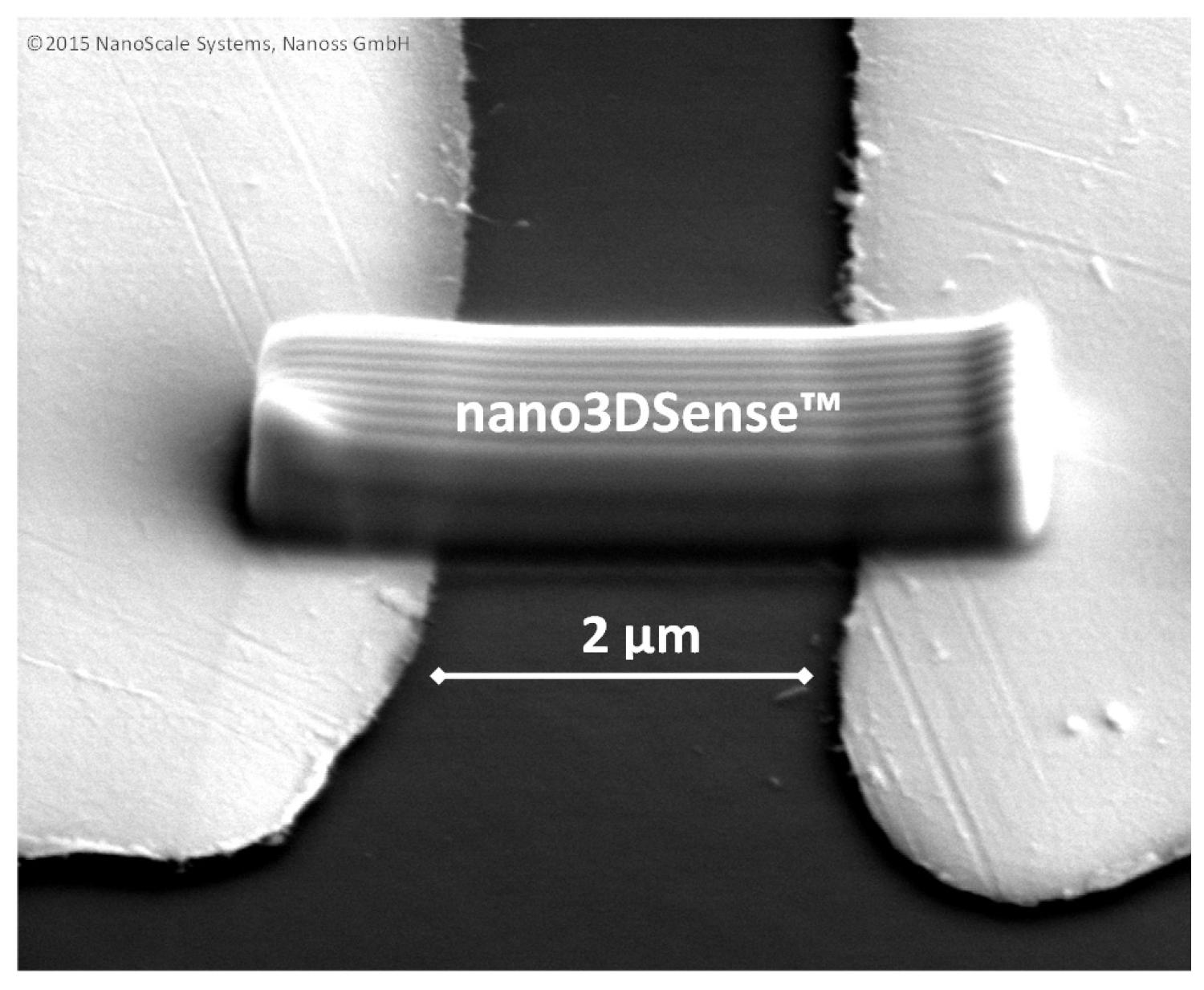
- A Nanosensor 3D Printed Using the Nano3DSense Machine. Available online: https://nanoss.de/wp-content/uploads/2015/01/EBID_Force_strain1.jpg (accessed on 25 April 2024).
- Kotz, F.; Quick, A.S.; Risch, P.; Martin, T.; Hoose, T.; Thiel, M.; Helmer, D.; Rapp F Kotz, B.E.; Risch, P.; Helmer, D.; et al. Two-Photon Polymerization of Nanocomposites for the Fabrication of Transparent Fused Silica Glass Microstructures. Adv. Mater. 2021, 33, 2006341. [Google Scholar] [CrossRef] [PubMed]
- Lee, S.; Lee, D.W.; Rajput, N.; Levato, T.; Shanti, A.; Kim, T.Y. 3D-Printed Microcubes for Catalase Drug Delivery. ACS Omega 2023, 8, 26775–26781. [Google Scholar] [CrossRef] [PubMed]
- 3D Printed Microneedles Allowing Promising Major Advancement in Biomedical Field. Available online: https://www.nanoscribe.com/fileadmin/Nanoscribe/Applications/Life_sciences/QuantumX-bio-needles_Gallery.jpg (accessed on 25 April 2024).
- Microscopic Image Showing Capability of D4200S. Available online: https://nano3dprint.com/wp-content/uploads/2022/09/dline1.jpg (accessed on 25 April 2024).
- Hamid Allah, A.; Eyebe, G.A.; Domingue, F. Fully 3D-Printed Microfluidic Substrate Integrated Waveguide Based Sensor for in Vitro Diagnostics of Diabetes. In Proceedings of the 2023 53rd European Microwave Conference (EuMC), Berlin, Germany, 19 September 2023; pp. 560–563. [Google Scholar]
- A Fully Functional Electronic Device Manufactured by DragonFly IV. Available online: https://www.nano-di.com/wp-content/uploads/2022/02/002-JAMES-AME-Motor-Logo.png (accessed on 25 April 2024).
- Fidan, I.; Huseynov, O.; Alshaikh Ali, M.; Alkunte, S.; Rajeshirke, M.; Gupta, A.; Hasanov, S.; Tantawi, K.; Yasa, E.; Yilmaz, O.; et al. Recent Inventions in Additive Manufacturing: Holistic Review. Inventions 2023, 8, 103. [Google Scholar] [CrossRef]
- Hengsteler, J.; Kanes, K.A.; Khasanova, L.; Momotenko, D. Beginner’s Guide to Micro- and Nanoscale Electrochemical Additive Manufacturing. Annu. Rev. Anal. Chem. 2023, 16, 71–91. [Google Scholar] [CrossRef] [PubMed]
- Seok, I.; Kilula, D.; Guo, Z. Micro/Nanoscale 3-Dimensional Fabrication Using Multi-Photons Polymerization: Review. ES Mater. Manuf. 2023, 21, 849. [Google Scholar] [CrossRef]
- Sadoun, A.M.; Mohammed, M.M.; Elsayed, E.M.; Meselhy, A.F.; El-Kady, O.A. Effect of Nano Al2O3 Coated Ag Addition on the Corrosion Resistance and Electrochemical Behavior of Cu-Al2O3 Nanocomposites. J. Mater. Res. Technol. 2020, 9, 4485–4493. [Google Scholar] [CrossRef]
- Li, Q.; Kulikowski, J.; Doan, D.; Tertuliano, O.A.; Zeman, C.J.; Wang, M.M.; Schatz, G.C.; Gu, X.W. Mechanical Nanolattices Printed Using Nanocluster-Based Photoresists. Science 2022, 378, 768–773. [Google Scholar] [CrossRef] [PubMed]
- Hasanov, S.; Alkunte, S.; Rajeshirke, M.; Gupta, A.; Huseynov, O.; Fidan, I.; Alifui-Segbaya, F.; Rennie, A. Review on Additive Manufacturing of Multi-Material Parts: Progress and Challenges. J. Manuf. Mater. Process. 2021, 6, 4. [Google Scholar] [CrossRef]
- Roig, A.; Ramis, X.; De la Flor, S.; Serra, À. Eugenol-Based Dual-Cured Materials with Multiple Dynamic Exchangeable Bonds. Eur. Polym. J. 2024, 206, 112782. [Google Scholar] [CrossRef]
- Binyamin, I.; Grossman, E.; Gorodnitsky, M.; Kam, D.; Magdassi, S.; Binyamin, I.; Gorodnitsky, M.; Kam, D.; Magdassi, S.; Grossman, E. 3D Printing Thermally Stable High-Performance Polymers Based on a Dual Curing Mechanism. Adv. Funct. Mater. 2023, 33, 2214368. [Google Scholar] [CrossRef]
- Reizabal, A.; Tandon, B.; Lanceros-Méndez, S.; Dalton, P.D. Electrohydrodynamic 3D Printing of Aqueous Solutions. Small 2023, 19, 2205255. [Google Scholar] [CrossRef] [PubMed]
- Lee, G.H.; Lee, Y.R.; Kim, H.; Kwon, D.A.; Kim, H.; Yang, C.; Choi, S.Q.; Park, S.; Jeong, J.W.; Park, S. Rapid Meniscus-Guided Printing of Stable Semi-Solid-State Liquid Metal Microgranular-Particle for Soft Electronics. Nat. Commun. 2022, 13, 2643. [Google Scholar] [CrossRef] [PubMed]
- Kumar, A.; Pandey, P.M.; Jha, S.; Banerjee, S.S. Experimental Investigations into Additive Manufacturing of Styrene-Ethylene-Butylene-Styrene Block Copolymers Using Solvent Cast 3D Printing Technique. Rapid Prototyp. J. 2023, 29, 1367–1385. [Google Scholar] [CrossRef]
- Weidinger, B.; Yang, G.; von Coelln, N.; Nirschl, H.; Wacker, I.; Tegeder, P.; Schröder, R.R.; Blasco, E. 3D Printing Hierarchically Nano-Ordered Structures. Adv. Sci. 2023, 10, 2302756. [Google Scholar] [CrossRef]
- Hengsteler, J.; Mandal, B.; Van Nisselroy, C.; Lau, G.P.S.; Schlotter, T.; Zambelli, T.; Momotenko, D. Bringing Electrochemical Three-Dimensional Printing to the Nanoscale. Nano Lett. 2021, 21, 9093–9101. [Google Scholar] [CrossRef]
- Liu, H.; He, L.; Kuzmanović, M.; Huang, Y.; Zhang, L.; Zhang, Y.; Zhu, Q.; Ren, Y.; Dong, Y.; Cardon, L.; et al. Advanced Nanomaterials in Medical 3D Printing. Small Methods 2024, 8, 2301121. [Google Scholar] [CrossRef]
- Kampleitner, C.; Changi, K.; Felfel, R.M.; Scotchford, C.A.; Sottile, V.; Kluger, R.; Hoffmann, O.; Grant, D.M.; Epstein, M.M. Preclinical Biological and Physicochemical Evaluation of Two-Photon Engineered 3D Biomimetic Copolymer Scaffolds for Bone Healing. Biomater Sci 2020, 8, 1683–1694. [Google Scholar] [CrossRef] [PubMed]
- Muhindo, D.; Elkanayati, R.; Srinivasan, P.; Repka, M.A.; Ashour, E.A. Recent Advances in the Applications of Additive Manufacturing (3D Printing) in Drug Delivery: A Comprehensive Review. AAPS PharmSciTech 2023, 24, 57. [Google Scholar] [CrossRef] [PubMed]
- Rahman, M.H.; Liza, N.Y.; Hossain, K.R.; Kalambhe, D.R.; Shyeed, M.A.; Noor, D.H. Additive Manufacturing in Nano Drug Delivery Systems. Pharm. Sci. Adv. 2024, 2, 100036. [Google Scholar] [CrossRef]
- Liu, J.; Liu, Y.; Deng, C.; Yu, K.; Fan, X.; Zhang, W.; Tao, Y.; Hu, H.; Deng, L.; Xiong, W. 3D Printing Nano-Architected Semiconductors Based on Versatile and Customizable Metal-Bound Composite Photoresins. Adv. Mater. Technol. 2022, 7, 2101230. [Google Scholar] [CrossRef]
- Bernasconi, R.; Hatami, D.; Hosseinabadi, H.N.; Zega, V.; Corigliano, A.; Suriano, R.; Levi, M.; Langfelder, G.; Magagnin, L. Hybrid Additive Manufacturing of a Piezopolymer-Based Inertial Sensor. Addit. Manuf. 2022, 59, 103091. [Google Scholar] [CrossRef]
- Chai, N.; Yue, Y.; Chen, X.; Zeng, Z.; Li, S.; Wang, X. Isotropic Sintering Shrinkage of 3D Glass-Ceramic Nanolattices: Backbone Preforming and Mechanical Enhancement. Int. J. Extrem. Manuf. 2024, 6, 025003. [Google Scholar] [CrossRef]
- Gailevičius, D.; Padolskytė, V.; Mikoliūnaitė, L.; Šakirzanovas, S.; Juodkazis, S.; Malinauskas, M. Additive-Manufacturing of 3D Glass-Ceramics down to Nanoscale Resolution. Nanoscale Horiz. 2019, 4, 647–651. [Google Scholar] [CrossRef]


Disclaimer/Publisher’s Note: The statements, opinions and data contained in all publications are solely those of the individual author(s) and contributor(s) and not of MDPI and/or the editor(s). MDPI and/or the editor(s) disclaim responsibility for any injury to people or property resulting from any ideas, methods, instructions or products referred to in the content. |
© 2024 by the authors. Licensee MDPI, Basel, Switzerland. This article is an open access article distributed under the terms and conditions of the Creative Commons Attribution (CC BY) license (https://creativecommons.org/licenses/by/4.0/).
Share and Cite
Fidan, I.; Alshaikh Ali, M.; Naikwadi, V.; Gudavasov, S.; Mahmudov, M.; Mohammadizadeh, M.; Zhang, Z.; Sharma, A. Nano-Level Additive Manufacturing: Condensed Review of Processes, Materials, and Industrial Applications. Technologies 2024, 12, 117. https://doi.org/10.3390/technologies12070117
Fidan I, Alshaikh Ali M, Naikwadi V, Gudavasov S, Mahmudov M, Mohammadizadeh M, Zhang Z, Sharma A. Nano-Level Additive Manufacturing: Condensed Review of Processes, Materials, and Industrial Applications. Technologies. 2024; 12(7):117. https://doi.org/10.3390/technologies12070117
Chicago/Turabian StyleFidan, Ismail, Mohammad Alshaikh Ali, Vivekanand Naikwadi, Shamil Gudavasov, Mushfig Mahmudov, Mahdi Mohammadizadeh, Zhicheng Zhang, and Ankit Sharma. 2024. "Nano-Level Additive Manufacturing: Condensed Review of Processes, Materials, and Industrial Applications" Technologies 12, no. 7: 117. https://doi.org/10.3390/technologies12070117