Article

Influence of Homo- and Hetero-Junctions on the Propagation Characteristics of Love Waves in a Piezoelectric Semiconductor Semi-Infinite Medium

1
School of Mathematics and Physics, University of Science and Technology Beijing, Beijing 100083, China
2
Department of Applied Mechanics, University of Science and Technology Beijing, Beijing 100083, China
3
School of Civil and Resource Engineering, University of Science and Technology Beijing, Beijing 100083, China
*
Author to whom correspondence should be addressed.
Mathematics 2024, 12(7), 1075; https://doi.org/10.3390/math12071075
Submission received: 22 February 2024 / Revised: 19 March 2024 / Accepted: 27 March 2024 / Published: 2 April 2024
(This article belongs to the Special Issue Modeling and Analyses in Advanced Materials)

Abstract

:
With the fast development and miniaturization of acoustic and electric smart devices, micro and nanoscale piezoelectric semiconductor materials are gradually being used to manufacture information communication, energy conversion, and nondestructive testing technologies. As the core components of the above piezoelectric semiconductor devices, homo- and hetero-junctions have an evident influence on the propagation performance of high-frequency and short-wavelength elastic waves inside the bulk piezoelectric semiconductor materials. Based on the Gurtin–Murdoch theory, a theoretical model of interface effect originating from homo- and hetero-junctions is established to investigate the propagation properties of Love waves in a piezoelectric semiconductor semi-infinite medium considering the electrical open circuit (insulation) and short circuit (metalized ground) surface boundary conditions and biasing electric fields. Four interface characteristic lengths are introduced to describe the electrical imperfect interface of homo- and hetero-junctions, which are legitimately confirmed through comparisons of the dispersion and attenuation curves of Love waves. The influence of homo- and hetero-junctions on the dispersion and attenuation characteristics of Love waves are elaborated in detail. Numerical results show that the interface characteristic lengths are independent of the electrical surface boundary conditions, acceptor and donor concentrations, thickness of the upper piezoelectric semiconductor layer, and biasing electric fields in the piezoelectric semiconductor semi-infinite medium. Moreover, the propagation characteristics of Love waves can be manipulated by changing the biasing electric field parallel to the homo- and hetero-junctions. Since the high-frequency and short-wavelength Love wave is an important class of surface acoustic waves propagating in micro- and nano-scale piezoelectric semiconductor materials, the establishment of mathematical models and the revelation of physical mechanisms are fundamental to the analysis and optimization of the above piezoelectric semiconductor devices.

1. Introduction

Due to the piezoelectric and semiconductor effects, the deformations in piezoelectric semiconductor (PSC) materials resulting from the propagation of bulk, surface, and interface elastic waves can lead to the interaction between the mechanical displacement, electric potential, perturbation of carrier concentration [1,2,3]. Linear partial differential equations can be used to mathematically describe the coupling relationship of the above physical quantities, including the linear constitutive and governing equations. Based on the classical partial differential solution theory, the wave motion physical quantities, such as stress, electric displacement, and carrier current density, can be solved accurately [4,5,6]. This provides a theoretical basis for PSC materials, such as zinc oxide (ZnO) nanoparticles, nanowires, nanotubes, and nanofilms [7,8], to be used for information communication, energy conversion, and nondestructive testing technologies [9,10,11,12]. Using different doping techniques, the majority of charge carriers in PSC materials can be holes or electrons, respectively, which are often referred to as p-type or n-type PSC materials. Due to the migration and diffusion of hole and electron carriers, a PN junction usually appears at the bonded interface between a p-type PSC material and an n-type PSC material. Some special semiconductor materials can be doped for p-type semiconductor materials and doped for n-type semiconductor materials, such as ZnO and silicon (Si). PN junctions can be classified as homo- and hetero-junctions, which are the core components of the above PSC devices, which can profoundly affect the physical properties of the PSC materials. Therefore, many researchers have studied the influence of PN junctions on the dynamic mechanical properties of PSC materials.
Fan et al. derived nonlinear governing equations on the electromechanical coupling and carrier concentrations for a static PN junction subjected to a pair of tensile/compressive stresses at the endpoints to investigate the adjustability and controllability on the fundamental characteristics of a PN junction by mechanical loading [13]. Numerical results indicate that a shorter distance between the loading point and the depletion layer can produce evident adjustment and control effects. Yang et al. discussed that the diffusion of non-equilibrium minority carriers under the influence of a piezo potential and the corresponding current–voltage characteristics of a PN junction exposed to mechanical loading [14], the whole-domain coupling between electromechanical fields and charge carriers inside a PN junction based on the traditional depletion layer approximation and the low injection assumption [15], and the effect of mechanical loadings on PN junction performance [16]. Liang et al. studied the electromechanical and electrical behaviors of a PN junction in a multiferroic composite fiber consisting of a PSC layer between two piezomagnetic layers under a transverse magnetic field [17]. It is found that a loading location closer to the space charge zone produces a stronger effect on the current–voltage characteristics of a PN junction, and the tuning effect of mechanical loadings depends on how much influence the deformation-induced electric field in proximity to a space charge zone. It is obtained that the linear analytical solution for the built-in potential and electric field in the PN junction when there is no applied voltage between the two ends of the fiber. It is found that the heterojunction is sensitive to the magnetic field with potential applications in piezotronics. Based on the macroscopic theory of thermopiezoelectric semiconductors, Cheng et al. derived a linearized one-dimensional model for thermally induced extensional deformation of the fibers to examine the effects of a uniform temperature change on PN junctions [18]. It is shown that homogeneous junctions have relatively good temperature stability, but heterogeneous junctions are sensitive to a temperature change that may be explored for thermally manipulating piezotronic devices. Guo et al. established the mathematical models of the propagation of radially propagated cylindrical surface waves in a PSC semi-infinite medium to investigate the influence of PN junctions on the dispersion and attenuation properties of the above waves [19]. It is found that PN junctions can be approximately treated as imperfect interfaces, which can enhance the width of band gaps of anti-plane elastic waves and the attenuation properties of surface waves, especially for high-frequency short-wavelength elastic waves. Yang et al. discussed the tuning mechanism of a mechanically induced artificial potential barrier on the performance of PN junctions [20]. It is found that the tensile-stress mode of the mechanically induced artificial potential barrier improves the performance of PN junctions by reconstructing the interface potential barrier and the compressive stress mode by stimulating strong interaction with the interface barrier. Fang et al. established a linearized one-dimensional model for the PSC fiber to study the electromechanical field under a pair of applied end mechanical forces and reveal the piezotronic performance modulation in the non-uniform PSC PN junction [21]. It is indicated that the acoustoelectric fields in the space charge region of the non-uniform PSC PN junction are more sensitive to the applied mechanical forces compared with that of the uniform junction, especially for a heterogeneous PN junction. Treated as an electrical gradient layer between the covering layer and the substrate, Xu et al. discussed the influence of PN junctions on the dispersion and attenuation characteristics of Love waves in PSC semi-infinite mediums [22]. It is found that the PN junction has an evident influence on the wave-mode shapes, electric potential, carrier concentration, electric displacement, and the current density of carriers of the above waves.
Based on the above research findings, it is known that the geometric thicknesses of PN junctions are usually on the order of micrometers. PN junctions often have physical properties that differ from those of bulk PSC materials. For example, the steady-state charge carrier concentrations in PN junctions show a gradient distribution. When the geometric sizes of the bulk PSC material are also on the order of micrometers, the PN junctions will have a significant impact on the propagation performance of high-frequency and short-wavelength elastic waves inside the bulk PSC materials. This happens to reflect the interface effect originating from the PN junctions in PSC materials, according to the Gurtin–Murdoch theory [23,24,25]; that is, the boundary conditions with imperfect interface parameters can be used to describe the discontinuous relationships of wave motion quantities on both sides of the interface [26,27]. Therefore, based on the above research content, this paper further proposes the theoretical model of interface effect originating from the PN junction and studies its influence on the propagation characteristics of Love waves in a PSC semi-infinite medium. First, considering the coupling mechanical displacement, electric potential, and charge carrier perturbation, it is mathematically derived that the basic equations of a PSC semi-infinite medium in Section 2, which consists of a lower PSC substrate, an upper PSC layer, and a PN junction, i.e., homo- or hetero-junction, that appears at the interface between these two regions. Two biasing electric fields are further considered in the basic equations of the lower n-type PSC substrate, which provides evident influence on the physical properties of the Schottky junction. Then, based on the Gurtin–Murdoch theory [24,25,26] and through the spectral method [28,29,30,31], two equivalent mathematical models are established to investigate the dispersion and attenuation characteristics of Love waves. Finally, based on the above two equivalent mathematical models, the numerical results of the dispersion and attenuation curves of shear horizontal waves are provided in Section 5. After that, the conclusion remarks are given in Section 6.

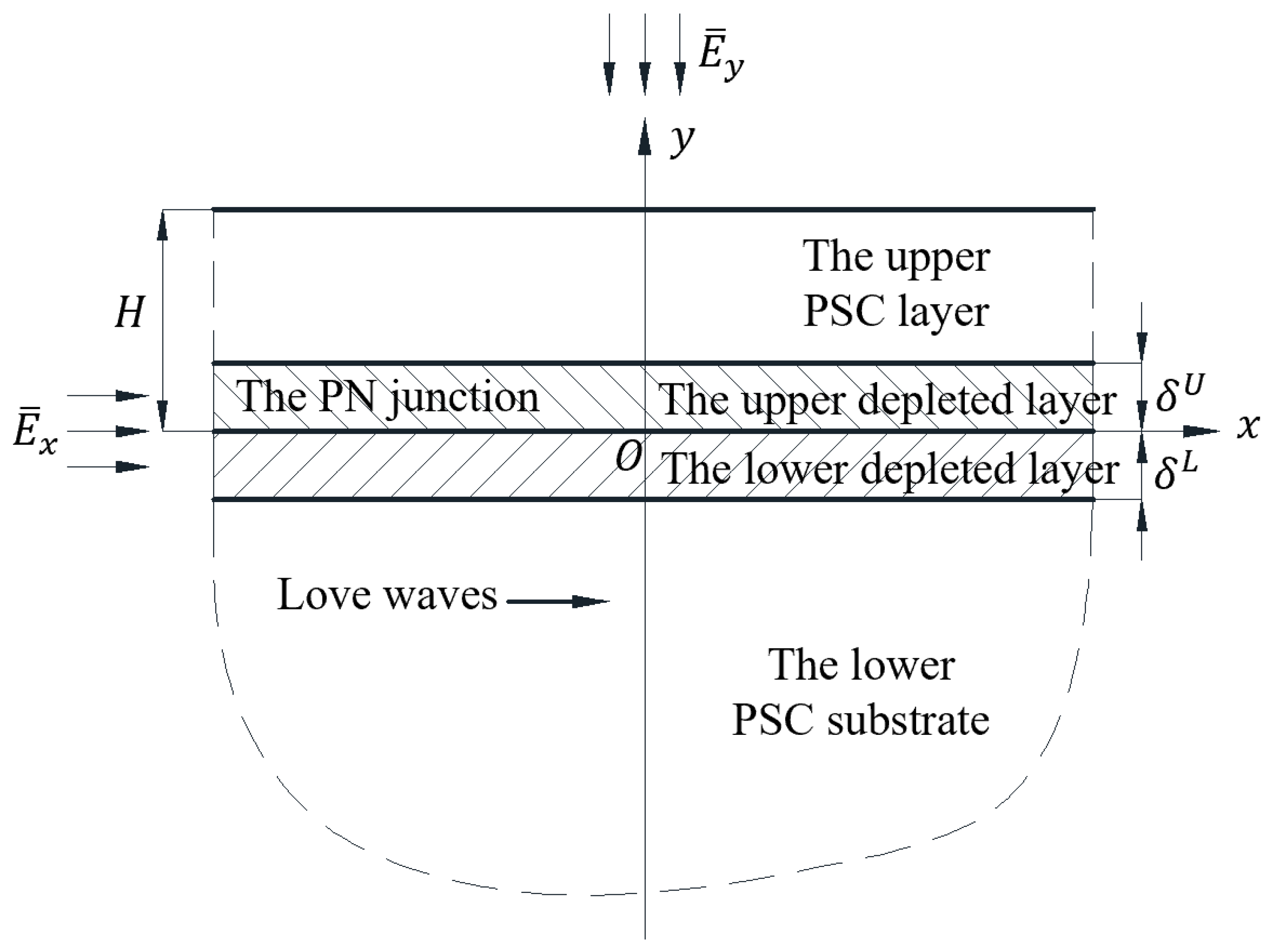
2. Problem Formulation and Basic Equations

Consider a PSC semi-infinite medium, which includes a low PSC substrate and an upper PSC layer, as shown in Figure 1. These two PSC regions are both transversely isotropic in the O x y plane. The z -direction is the polarization direction. The thickness of the upper PSC layer H is at the microscale. Both the upper PSC layer and lower PSC substrate are homogeneous and doped by different methods, in which the carrier concentrations and types are different. Therefore, a PN junction, i.e., homo- or hetero-junction, appears at the interface between these two PSC regions. It includes two depleted layers, in which the steady hole and electron carrier concentrations are inhomogeneous along the y axis. The geometrical thicknesses of these two depleted layers are δ U and δ L , respectively. Two biasing electric fields E ¯ x and E ¯ y are applied to the PSC semi-infinite medium. Consider the propagation of Love waves in this PSC semi-infinite medium in the O x y plane along the x axis. To establish the mathematical models of the propagation of Love waves, the basic equations of the upper PSC layer and the lower PSC substrate are mathematically derived in this section. In order to distinguish these two PSC regions in the latter formulation, the physical parameters of these two PSC regions are indicated by the superscripts “ U ” and “ L ”, respectively.
Under the supposition of small deformation and the quasi-static electric field approximation, the constitutive equations of the upper PSC layer and lower PSC substrate are [3,4]
σ i j U = c i j k l U u l , k U + e k i j U ϕ , k U ,
D k U = e k i j U u j , i U ε k l U ϕ , l U ,
J k U = q c ¯ U μ k l U ϕ , l U + q c U μ k l U E ¯ l + α U q d k l U c , l U ,
σ i j L = c i j k l L u l , k L + e k i j L ϕ , k L ,
D k L = e k i j L u j , i L ε k l L ϕ , l L ,
J k L = q c ¯ L μ k l L ϕ , l L + q c L μ k l L E ¯ l + α L q d k l L c , l L
where u l U , ϕ U , c U , σ i j U , D k U , and J k U are the mechanical displacement, electric potential, perturbation of carrier concentration, Cauchy stress, electric displacement, and carrier current density of the upper PSC layer, respectively, and u l L , ϕ L , c L , σ i j L , D k L , and J k L are the mechanical displacement, electric potential, perturbation of carrier concentration, Cauchy stress, electric displacement, and carrier current density of the lower PSC substrate, respectively. With consideration of the piezoelectric and semiconductor effects, c i j k l U , e k i j U , ε k l U , μ k l U , and d k l U are the elastic, piezoelectric, dielectric, carrier migration, and diffusion parameters of the upper PSC layer, respectively, and c i j k l L , e k i j L , ε k l L , μ k l L , and d k l L are the elastic, piezoelectric, dielectric, carrier migration, and diffusion parameters of the lower PSC substrate, respectively. The carrier charge is q = 1.602 × 10 19 C . For the combination of upper n-type PSC layer and lower p-type PSC substrate, the numerical values of the two constants are α U = 1 , α L = 1 ; the steady electron and hole carrier concentrations c ¯ U and c ¯ L [13] are
c ¯ U = { N D U δ U y H N D U e x p [ q μ y y U N D U d y y U ε y y U ( 1 2 y 2 δ U y + 1 2 δ U 2 ) 2 E ¯ y ( y δ U ) ] 0 y δ U ,
c ¯ L = { N A L e x p [ q μ y y L N A L d y y L ε y y L ( 1 2 y 2 + δ L y + 1 2 δ L 2 ) + 2 E ¯ y ( y + δ L ) ] δ L y 0 N A L < y δ L
where N D U and N A L are the donor and acceptor concentrations in the upper n-type PSC layer and lower p-type PSC substrate, respectively, and
δ U = 2 ε y y L N A L ε y y U d y y U q N D U ( ε y y L N A L + ε y y U N D U ) μ y y U l n N A L N D U n i U n i L ,
δ L = 2 ε y y L ε y y U N D U d y y L q N A L ( ε y y L N A L + ε y y U N D U ) μ y y L l n N A L N D U n i U n i L
where n i U and n i L are the intrinsic carrier concentrations of the upper n-type PSC layer and lower p-type PSC substrate, respectively. While for the combination of the upper p-type PSC layer and lower n-type PSC substrate, the numerical values of the two constants are α U = 1 , α L = 1 ; the steady hole and electron carrier concentrations c ¯ U and c ¯ L [13] are
c ¯ U = { N A U δ U y H N A U e x p [ q μ y y U N A U d y y U ε y y U ( 1 2 y 2 δ U y + 1 2 δ U 2 ) + 2 E ¯ y ( y δ U ) ] 0 y δ U ,
c ¯ L = { N D L e x p [ q μ y y L N D L d y y L ε y y L ( 1 2 y 2 + δ L y + 1 2 δ L 2 ) 2 E ¯ y ( y + δ L ) ] δ L y 0 N D L < y δ L
where N A U and N D L are the acceptor and donor concentrations in the upper p-type PSC layer and lower n-type PSC substrate, respectively, and
δ U = 2 ε y y L N D L ε y y U d y y U q N A U ( ε y y L N D L + N A U ε y y U ) μ y y U l n N A U N D L n i U n i L ,
δ L = 2 ε y y L ε y y U N A U d y y L q N D L ( N D L ε y y L + ε y y U N A U ) μ y y L l n N A U N D L n i U n i L
Based on plane strain assumption, the mechanical displacements, electric potential, and carrier concentration perturbations of Love waves are functions of space coordinates x and y and time coordinate t mathematically
{ u x U , u y U , u z U , ϕ U , c U } = { 0 , 0 , u z U ( x , y , t ) , ϕ U ( x , y , t ) , c U ( x , y , t ) } ,
{ u x L , u y L , u z L , ϕ L ,   c L } = { 0 , 0 , u z L ( x , y , t ) , ϕ L ( x , y , t ) , c L ( x , y , t ) }
Inserting Equation (6) into Equation (1) leads to non-zero wave motion quantities of Love waves
σ z x U = σ x z U = c z x z x U 𝜕 u z U 𝜕 x + e x x z U 𝜕 ϕ U 𝜕 x ,  
σ z y U = σ y z U = c z y z y U 𝜕 u z U 𝜕 y + e y y z U 𝜕 ϕ U 𝜕 y ,
D x U = e x x z U 𝜕 u z U 𝜕 x ε x x U 𝜕 ϕ U 𝜕 x ,  
D y U = e y y z U 𝜕 u z U 𝜕 y ε y y U 𝜕 ϕ U 𝜕 y ,
J x U = q c ¯ U μ x x U 𝜕 ϕ U 𝜕 x + q c U μ x x U E ¯ x + α U q d x x U 𝜕 c U 𝜕 x ,
J y U = q c ¯ U μ y y U 𝜕 ϕ U 𝜕 y + q c U μ y y U E ¯ y + α U q d y y U 𝜕 c U 𝜕 y ,
σ z x L = σ x z L = c z x z x L 𝜕 u z L 𝜕 x + e x x z L 𝜕 ϕ L 𝜕 x ,  
σ z y L = σ y z L = c z y z y L 𝜕 u z L 𝜕 y + e y y z L 𝜕 ϕ L 𝜕 y ,
D x L = e x x z L 𝜕 u z L 𝜕 x ε x x L 𝜕 ϕ L 𝜕 x ,  
D y L = e y y z L 𝜕 u z L 𝜕 y ε y y L 𝜕 ϕ L 𝜕 y ,
J x L = q c ¯ L μ x x L 𝜕 ϕ L 𝜕 x + q c L μ x x L E ¯ x + α L q d x x L 𝜕 c L 𝜕 x ,
J y L = q c ¯ L μ y y L 𝜕 ϕ L 𝜕 y + q c L μ y y L E ¯ y + α L q d y y L 𝜕 c L 𝜕 y
Based on the plane strain assumption, the governing equations of the upper PSC layer and lower PSC substrate [3,4] are
𝜕 σ x z U 𝜕 x + 𝜕 σ y z U 𝜕 y = ρ U 𝜕 2 u z U 𝜕 t 2 ,
𝜕 D x U 𝜕 x + 𝜕 D y L 𝜕 y = α U q c U ,
𝜕 J x U 𝜕 x + 𝜕 J y U 𝜕 y = α U q 𝜕 c U 𝜕 t
𝜕 σ x z L 𝜕 x + 𝜕 σ y z L 𝜕 y = ρ L 𝜕 2 u z L 𝜕 t 2 ,
𝜕 D x L 𝜕 x + 𝜕 D y L 𝜕 y = α L q c L ,
𝜕 J x L 𝜕 x + 𝜕 J y L 𝜕 y = α L q 𝜕 c L 𝜕 t
where ρ U and ρ L are the mass densities of the upper PSC layer and lower PSC substrate, respectively. Inserting Equations (7) into Equations (8) and (9) leads to
( c x z x z U 𝜕 2 𝜕 x 2 + c y z y z U 𝜕 2 𝜕 y 2 ) u z U + ( e x x z U 𝜕 2 𝜕 x 2 + e y y z U 𝜕 2 𝜕 y 2 ) ϕ U = ρ U 𝜕 2 u z U 𝜕 t 2 ,
( e x x z U 𝜕 2 𝜕 x 2 + e y y z U 𝜕 2 𝜕 y 2 ) u z U ( ε x x U 𝜕 2 𝜕 x 2 + ε y y U 𝜕 2 𝜕 y 2 ) ϕ U = α U q c U ,
[ μ x x U c ¯ U 𝜕 2 𝜕 x 2 + μ y y U ( c ¯ U 𝜕 2 𝜕 y 2 + c ¯ U 𝜕 𝜕 y ) ] ϕ U
+ ( μ x x U E ¯ x 𝜕 𝜕 x + μ y y U E ¯ y 𝜕 𝜕 y ) c U + ( d x x U 𝜕 2 𝜕 x 2 + d y y U 𝜕 2 𝜕 y 2 ) c U = α U q 𝜕 c U 𝜕 t
( c x z x z L 𝜕 2 𝜕 x 2 + c y z y z L 𝜕 2 𝜕 y 2 ) u z L + ( e x x z L 𝜕 2 𝜕 x 2 + e y y z L 𝜕 2 𝜕 y 2 ) ϕ L = ρ L 𝜕 2 u z L 𝜕 t 2 ,
( e x x z L 𝜕 2 𝜕 x 2 + e y y z L 𝜕 2 𝜕 y 2 ) u z L ( ε x x L 𝜕 2 𝜕 x 2 + ε y y L 𝜕 2 𝜕 y 2 ) ϕ L = α L q c L ,
[ μ x x L c ¯ L 𝜕 2 𝜕 x 2 + μ y y L ( c ¯ L 𝜕 2 𝜕 y 2 + c ¯ L 𝜕 𝜕 y ) ] ϕ L
+ ( μ x x L E ¯ x 𝜕 𝜕 x + μ y y L E ¯ y 𝜕 𝜕 y ) c L ( d x x L 𝜕 2 𝜕 x 2 + d y y L 𝜕 2 𝜕 y 2 ) c L = α L q 𝜕 c L 𝜕 t
On the surface y = H , consider two types of boundary conditions: the mechanical open circuit and electrical open circuit, i.e., displacement-free and insulation surface boundary condition [22]
{ N i σ i j U , N i D i U , N i J i U } | y = H = { 0 , 0 , 0 }
and the mechanical open circuit electrical short circuit, i.e., displacement-free and metalized ground surface boundary condition [22]
{ N i σ i j U , ϕ U , c U } | y = H = { 0 , 0 , 0 }
Inserting the surface normal vector N i = { 0 , 1 , 0 } into Equations (12) and (13) leads to
{ σ y z U , D y U , J y U } | y = H = { 0 , 0 , 0 }
{ σ y z U , ϕ U , c U } | y = H = { 0 , 0 , 0 }
Based on Equations (10), (11), (14) and (15), the mathematical model of the propagation of Love waves will be established through the spectral method to investigate the dispersion and attenuation characteristics of Love waves. However, as the core part of the PSC semi-infinite medium, the basic equations of the PN junction are not fully given. Therefore, when the PN junction is treated as an electrical imperfect interface or an electrical gradient layer, two different groups of basic equations can be given, and two equivalent mathematical models can be established in Section 3 and Section 4. To improve the computational efficiency of these two mathematical models, we reasonably modify some calculating intervals of definite integrals in the spectral method.

3. The First Equivalent Mathematical Model

According to Equation (6), assume the mathematical expressions of the displacement, electric potential, and carrier concentration perturbation of Love wave in the upper PSC layer and lower PSC substrate as
{ u z U , ϕ U , c U } = { U z U ( y ) , U ϕ U ( y ) , U c U ( y ) } e x p [ i ( k U x ω U t ) ]
{ u z U , ϕ L , c L } = { U z L ( y ) , U ϕ L ( y ) , U c L ( y ) } e x p [ i ( k L x ω L t ) ]
where k U and ω U are the apparent wave number component and angular frequency of the upper PSC layer, respectively, and k L and ω L are the apparent wave number component and angular frequency of the lower PSC substrate, respectively. Based on the spectral method [28,29,30,31], the Legendre polynomials are used to expand the three undetermined amplitudes U z U , U ϕ , and U c U in the upper PSC layer
{ U z U ( y ) , U ϕ U ( y ) , U c U ( y ) } = { m = 0 M z m U R m U ( y ) ,
m = 0 M ϕ m U R m U ( y ) , m = 0 M c m U R m U ( y ) } , 0 y H
where z m U , ϕ m U and c m U are expansion coefficients, m = 0 , 1 , 2 , , M . M is an integer and
R m U ( y ) = P m ( 2 y H H ) ,
P m ( y ¯ ) = d m 2 m m ! d y ¯ m ( y ¯ 2 1 ) m
the Laguerre polynomials are used to expand the three undetermined amplitudes U z L , U ϕ L , and U c L in the lower PSC substrate
{ U z L ( y ) , U ϕ L ( y ) , U c L ( y ) } = { m = 0 M z m L R m L ( y ) ,
m = 0 M ϕ m L R m L ( y ) , m = 0 M c m L R m L ( y ) } , < y 0
where z m L , ϕ m L and c m L are expansion coefficients and
R m L ( y ) = e y 2 L m ( y ) ,
R m L ( ) = R m L ( ) = 0 ,
L m ( y ¯ ) = e y ¯ m ! d m d y ¯ m ( y ¯ m e y ¯ )
Inserting Equations (16) and (18) into Equation (10), multiplying both sides by R j U ( y ) , and taking the definite integral over the interval 0 y H leads to
k 2 ( c y z y z U m = 0 M z m U 0 H R m U ( y ) R j U ( y ) d y + e y y z U m = 0 M ϕ m U 0 H R m U ( y ) R j U ( y ) d y )
+ c y z y z U m = 0 M z m U 0 H R m U ( y ) R j U ( y ) d y + e y y z U m = 0 M ϕ m U 0 H R m U ( y ) R j U ( y ) d y
= ρ U ω 2 m = 0 M z m U 0 H R m U ( y ) R j U ( y ) d y
k 2 ( e y y z U m = 0 M z m U 0 H R m U ( y ) R j U ( y ) d y ε y y U m = 0 M ϕ m U 0 H R m U ( y ) R j U ( y ) d y )
+ e y y z U m = 0 M z m U 0 H R m U ( y ) R j U ( y ) d y ε y y U m = 0 M ϕ m U 0 H R m U ( y ) R j U ( y ) d y
= α U q m = 0 M c m U 0 H R m U ( y ) R j U ( y ) d y
k 2 ( μ y y U N D U m = 0 M ϕ m U 0 H R m U ( y ) R j U ( y ) d y α U d y y U m = 0 M c m U 0 H R m U ( y ) R j U ( y ) d y )
+ i k μ y y U E ¯ x m = 0 M c m U 0 H R m U ( y ) R j U ( y ) d y μ y y U N D U m = 0 M ϕ m U 0 H R m U ( y ) R j U ( y ) d y
+ m = 0 M c m U ( μ y y U E ¯ y 0 H R m U ( y ) R j U ( y ) d y + α U d y y U 0 H R m U ( y ) R j U ( y ) d y )
= α U i ω m = 0 M c m U 0 H R m U ( y ) R j U ( y ) d y
Inserting Equations (17) and (20) into Equation (11), multiplying both sides by R j L ( y ) , and taking the definite integral over the interval < y 0 leads to
k 2 ( c y z y z L m = 0 M z m L 0 R m L ( y ) R j L ( y ) d y + e y y z L m = 0 M ϕ m L 0 R m L ( y ) R j L ( y ) d y )
+ c y z y z L m = 0 M z m L 0 R m L ( y ) R j L ( y ) d y + e y y z L m = 0 M ϕ m L 0 R m L ( y ) R j L ( y ) d y
= ρ L ω 2 m = 0 M z m L 0 R m L ( y ) R j L ( y ) d y
k 2 ( e y y z L m = 0 M z m L 0 R m L ( y ) R j L ( y ) d y ε y y L m = 0 M ϕ m L 0 R m L ( y ) R j L ( y ) d y )
+ e y y z L m = 0 M z m L 0 R m L ( y ) R j L ( y ) d y ε y y L m = 0 M ϕ m L 0 R m L ( y ) R j L ( y ) d y
= α L q m = 0 M c m L 0 R m L ( y ) R j L ( y ) d y
k 2 ( μ y y L N A L m = 0 M ϕ m L 0 R m L ( y ) R j L ( y ) d y α L d y y L m = 0 M c m L 0 R m L ( y ) R j L ( y ) d y )
+ i k μ y y L E ¯ x m = 0 M c m L 0 R m L ( y ) R j L ( y ) d y μ y y L N A L m = 0 M ϕ m L 0 R m L ( y ) R j L ( y ) d y
+ m = 0 M c m L ( μ y y L E ¯ y 0 R m L ( y ) R j L ( y ) d y + α L d y y L 0 R m L ( y ) R j L ( y ) d y )
= α L i ω m = 0 M c m L 0 R m L ( y ) R j L ( y ) d y
Inserting Equations (16) and (18) into Equations (14) and (15) and multiplying both sides R j U ( H ) or R j U ( H ) lead to
c z y z y U m = 0 M z m U R m U ( H ) R j U ( H ) + e y y z U m = 0 M ϕ m U R m U ( H ) R j U ( H ) = 0 ,
e y y z U m = 0 M z m U R m U ( H ) R j U ( H ) ε y y U m = 0 M ϕ m U R m U ( H ) R j U ( H ) = 0 ,
N D U μ y y U m = 0 M ϕ m U R m U ( H ) R j U ( H ) + μ y y U E ¯ y m = 0 M c m U R m U ( H ) R j U ( H )
+ α U d y y U m = 0 M c m U R m U ( H ) R j U ( H ) = 0
c z y z y U m = 0 M z m U R m U ( H ) R j U ( H ) + e y y z U m = 0 M ϕ m U R m U ( H ) R j U ( H ) = 0 ,
m = 0 M ϕ m U R m U ( H ) R j U ( H ) = 0 ,
m = 0 M c m U R m U ( H ) R j U ( H ) = 0
Considering the geometrical thickness of the PN junction is much smaller than that of the upper PSC layer, i.e., δ U + δ L < H , the PN junction is treated as a two-dimensional electrical imperfect interface without geometrical thickness but with piezoelectric and semiconductor effects in this mathematical model. Therefore, the mechanical displacement, electric potential, perturbation of carrier concentration, and Cauchy stress at the electrically imperfect interface are all continuous
{ u j U , ϕ U } | y = 0 + = { u j L , ϕ L } | y = 0 = { u j I , ϕ I } ,
{ c U , N i σ i j U } | y = 0 + = { c L , N i σ i j L } | y = 0
where u j I and ϕ I are the interface mechanical displacement vector and electric potential scalar, respectively. While the electric displacement and charge carrier current densities at the electrical imperfect interface are all discontinuous
{ N i D i U , N i J i U } | y = 0 + { N i D i L , N i J i L } | y = 0 = { D k , k I , J k , k p I + J k , k n I }
where D i I , J i p I , and J i n I are the interface electric displacement, hole and electron carrier current densities, respectively
D k I = e k i j I u j , i I ε k l I ϕ , l I ,
J k p I = q p ¯ I μ k l p I ϕ , l I + q p I μ k l p I E ¯ l q d k l p I p , l I ,
J k n I = q n ¯ I μ k l n I ϕ , l I + q n I μ k l n I E ¯ l + q d k l n I n , l I ,
where p ¯ I , n ¯ I , p I , n I , e k i j I , ε k l I , μ k l p I , μ k l n I , d k l p I , and d k l n I are the interface steady hole and electron carrier concentrations, perturbations of hole and electron carrier concentrations, piezoelectric and dielectric parameters, hole and electron carrier migration and diffusion parameters, respectively
{ n ¯ I , p ¯ I , e k i j I , ε k l I , p I , n I , μ k l n I , μ k l p I , d k l n I , d k l p I } = { 0 δ U c ¯ U d y , δ L 0 c ¯ L d y , f e U e k i j U + f e L e k i j L ,
f ε U ε k l U + f ε L ε k l L , δ L c L , δ U n U , μ k l U , μ k l L , d k l U , d k l L }
for the combination of upper p-type PSC layer and lower n-type PSC substrate and
{ p ¯ I , n ¯ I , e k i j I , ε k l I , n I , p I , μ k l p I , μ k l n I , d k l p I , d k l n I } = { 0 δ U c ¯ U d y , δ L 0 n ¯ L d y , f e U e k i j U + f e L e k i j L ,
f ε U ε k l U + f ε L ε k l L , δ L c L , δ U c U , μ k l U , μ k l L , d k l U , d k l L }
for the combination of upper p-type PSC layer and lower n-type PSC substrate, where f e U , f e L , f ε U , and f ε L are the interface characteristic lengths related to the interface piezoelectric and dielectric parameters, respectively. It should be noted that if the numerical values of the above four parameters are zero, the electrical imperfect interface is reduced to the electrical perfect interface [26,27]. Inserting the surface normal vector N i = { 0 , 1 , 0 } and Equations (33) and (34) into Equations (31) and (32) leads to
{ u z U , ϕ U , c U , σ y z U , D y U , J y U } | y = 0 + { u z L , ϕ L , c L , σ y z L , D y L , J y L } | y = 0
= { 0 , 0 , 0 , 0 , k L 2 ( f e U e x x z U + f e L e x x z L ) u z L + k L 2 ( f ε U ε x x U + f ε L ε x x L ) ϕ L ,
k L 2 q ( p ¯ I μ x x p I + n ¯ I μ x x n I ) ϕ L + i k L q ( μ x x L δ L + μ x x U δ U ) E ¯ x c L
k L 2 q ( d x x L δ L + d x x U δ U ) c L } | y = 0
Inserting Equations (16)–(18) and (20) into Equation (35) and multiplying both sides R j U ( 0 ) or R j L ( 0 ) lead to
m = 0 M z m U R m U ( 0 ) R j U ( 0 ) = m = 0 M z m L R m L ( 0 ) R j U ( 0 ) ,
m = 0 M ϕ m U R m U ( 0 ) R j U ( 0 ) = m = 0 M ϕ m L R m L ( 0 ) R j U ( 0 ) ,
m = 0 M c m U R m U ( 0 ) R j U ( 0 ) = m = 0 M c m L R m L ( 0 ) R j U ( 0 ) ,
c z y z y U m = 0 M z m U R m U ( 0 ) R j L ( 0 ) + e y y z U m = 0 M ϕ m U R m U ( 0 ) R j L ( 0 )
= c z y z y L m = 0 M z m L R m L ( 0 ) R j L ( 0 ) + e y y z L m = 0 M ϕ m L R m L ( 0 ) R j L ( 0 ) ,
e y y z U m = 0 M z m U R m U ( 0 ) R j L ( 0 ) ε y y U m = 0 M ϕ m U R m U ( 0 ) R j L ( 0 )
= e y y z L m = 0 M z m L R m L ( 0 ) R j L ( 0 ) ε y y L m = 0 M ϕ m L R m L ( 0 ) R j L ( 0 )
k 2 ( f e U e x x z U + f e L e x x z L ) m = 0 M z m L R m L ( 0 ) R j L ( 0 )
+ k 2 ( f ε U ε x x U + f ε L ε x x L ) m = 0 M ϕ m L R m L ( 0 ) R j L ( 0 ) ,
μ y y U N D U m = 0 M ϕ m U R m U ( 0 ) R j L ( 0 ) + μ y y U E ¯ y m = 0 M c m U R m U ( 0 ) R j L ( 0 )
+ α U d y y U m = 0 M c m U R m U ( 0 ) R j L ( 0 ) = μ y y L N A U m = 0 M ϕ m L R m L ( 0 ) R j L ( 0 )
+ μ y y L E ¯ y m = 0 M c m L R m L ( 0 ) R j L ( 0 ) + α L d y y L m = 0 M c m L R m L ( 0 ) R j L ( 0 )
+ k 2 ( p ¯ I μ x x p I + n ¯ I μ x x n I ) m = 0 M ϕ m L R m L ( 0 ) R j L ( 0 )
+ i k ( μ x x L δ L + μ x x U δ U ) E ¯ x m = 0 M c m L R m L ( 0 ) R j L ( 0 )
k 2 ( d x x L δ L + d x x U δ U ) m = 0 M c m L R m L ( 0 ) R j L ( 0 )
and
{ k U , ω U } = { k L , ω L } = { k , ω }
Inserting Equations (28), (29) and (36) into Equations (22)–(24) and (25)–(27) and letting j changes from 0 to M lead to
k 2 A ¯ P + k B ¯ P + C ¯ P = D ¯ P
where the unknown expansion coefficients vector is
P = { z 0 U , z 1 U , , z M U , ϕ 0 U , ϕ 1 U , , ϕ M U , c 0 U , c 1 U , , c M U ,   z 0 L , z 1 L , , z M L , ϕ 0 L , ϕ 1 L , , ϕ M L , c 0 L , c 1 L , , c M L } T
The explicit expressions of coefficient matrices A ¯ , B ¯ , C ¯ , and D ¯ in Equation (38) are given in Appendix A. In order to obtain the dispersion relation of Love waves, define another vector as
P ˜ = k P
Inserting Equation (40) into Equation (38) leads to
A ¯ P ˜ + k B ¯ P = ( D ¯ C ¯ ) P
Combining Equations (40) and (41) leads to
[ O E D ¯ C ¯ O ] { P P ˜ } = k [ E O B ¯ A ¯ ] { P P ˜ }
where O is the null matrix, and E is the unit matrix. Equation (42) is a generalized eigenvalue problem for the apparent wave number component k . Given the numerical values of the angular frequency of the shear horizontal wave ω, the dispersion and attenuation curves of Love waves can be obtained. Since many elements of matrices A ¯ , B ¯ , C ¯ , and D ¯ are related to the definite integrals of Legendre and Laguerre polynomials, the analytical results of the definite integrals of the above two polynomials are given in Appendix A of this paper. Using these analytical results, the generalized eigenvalue problem in Equation (41) can be calculated efficiently. However, to obtain the dispersion and attenuation curves of the shear horizontal wave, the interface characteristic lengths f e U , f e L , f ε U , and f ε L should be legitimately confirmed. To legitimately confirm the interface characteristic lengths f e U , f e L , f ε U , and f ε L another equivalent mathematical model is established in Section 4, i.e., the second mathematical model.

4. The Second Equivalent Mathematical Model

In this mathematical model, the PN junction is theoretically treated as an electrical gradient layer, in which the steady electron carrier concentration is a function of the space coordinate y and the vertical biasing electric field E ¯ y mathematically, as shown in Equations (2) and (3). Therefore, Equations (24) and (27) are modified as
k 2 ( μ y y U m = 0 M ϕ m U 0 H c ¯ U ( y ) R m U ( y ) R j U ( y ) d y α U d y y U m = 0 M c m U 0 H R m U ( y ) R j U ( y ) d y )
+ i k μ y y U E ¯ x m = 0 M c m U 0 H R m U ( y ) R j U ( y ) d y
μ y y U m = 0 M ϕ m U 0 H ( c ¯ U ( y ) R m U ( y ) + c ¯ U ( y ) R m U ( y ) ) R j U ( y ) d y
+ m = 0 M c m U ( μ y y U E ¯ y 0 H R m U ( y ) R j U ( y ) d y + α U d y y U 0 H R m U ( y ) R j U ( y ) d y )
= α U i ω m = 0 M c m U 0 H R m U ( y ) R j U ( y ) d y
k 2 ( μ y y L m = 0 M ϕ m L 0 c ¯ L ( y ) R m L ( y ) R j L ( y ) d y α L d y y L m = 0 M c m L 0 R m L ( y ) R j L ( y ) d y )
+ i k μ y y L E ¯ x m = 0 M c m L 0 R m L ( y ) R j L ( y ) d y
μ y y L m = 0 M ϕ m L 0 ( c ¯ L ( y ) R m L ( y ) + c ¯ L ( y ) R m L ( y ) ) R j L ( y ) d y
+ μ y y L E ¯ y m = 0 M c m L 0 R m L ( y ) R j L ( y ) d y + α L d y y L m = 0 M c m L 0 R m L ( y ) R j L ( y ) d y
= α L i ω m = 0 M c m L 0 R m L ( y ) R j L ( y ) d y
At the boundary y = 0 , consider the following interface condition
{ u j U , ϕ U , c U , N i σ i j U , N i D i U , N i J i U } | y = 0 + = { u j L , ϕ L , c L , N i σ i j L , N i D i L , N i J i L } | y = 0
Inserting the interface normal vector N i = { 0 , 1 , 0 } into Equation (45) leads to
{ u z U , ϕ U , c U , σ y z U , D y U , J y U } | y = 0 + = { u z U , ϕ L , c L , σ y z L , D y L , J y L } | y = 0
Inserting Equations (16)–(18) and (20) into Equation (46) and multiplying both sides R j L ( 0 ) or R j L ( 0 ) lead to
m = 0 M z m U R m U ( 0 ) R j L ( 0 ) = m = 0 M z m L R m L ( 0 ) R j L ( 0 ) ,
m = 0 M ϕ m U R m U ( 0 ) R j L ( 0 ) = m = 0 M ϕ m L R m L ( 0 ) R j L ( 0 ) ,
m = 0 M c m U R m U ( 0 ) R j L ( 0 ) = m = 0 M c m L R m L ( 0 ) R j L ( 0 ) ,
c z y z y U m = 0 M z m U R m U ( 0 ) R j U ( 0 ) + e y y z U m = 0 M ϕ m U R m U ( 0 ) R j U ( 0 )
= c z y z y L m = 0 M z m L R m L ( 0 ) R j L ( 0 ) + e y y z L m = 0 M ϕ m L R m L ( 0 ) R j L ( 0 ) ,
e y y z U m = 0 M z m U R m U ( 0 ) R j L ( 0 ) ε y y U m = 0 M ϕ m U R m U ( 0 ) R j L ( 0 )
= e y y z L m = 0 M z m L R m L ( 0 ) R j L ( 0 ) ε y y L m = 0 M ϕ m L R m L ( 0 ) R j L ( 0 ) ,
μ y y U c ¯ U ( 0 ) m = 0 M ϕ m U R m U ( 0 ) R j L ( 0 ) + μ y y U E ¯ y m = 0 M c m U R m U ( 0 ) R j L ( 0 )
+ α U d y y U m = 0 M c m U R m U ( 0 ) R j L ( 0 ) = μ y y L c ¯ L ( 0 ) m = 0 M ϕ m L R m L ( 0 ) R j L ( 0 )
+ μ y y L E ¯ y m = 0 M c m L R m L ( 0 ) R j L ( 0 ) + α L d y y L m = 0 M c m L R m L ( 0 ) R j L ( 0 )
Inserting Equations (28), (29) and (47) into Equations (22), (23), (25), (26), (43) and (44) and letting j changes from 0 to M lead to
k 2 A P + k B P + C P = D P
The explicit expressions of coefficient matrices A , B , C , and D in Equation (48) are given in Appendix A. Combining Equations (40) and (48) leads to
[ O E D C O ] { P P ˜ } = k [ E O B A ] { P P ˜ }
Equation (49) is also a generalized eigenvalue problem for the apparent wave number component k without the interface characteristic lengths. Considering these two mathematical models established in Section 3 and Section 4 are equivalent, the interface characteristic lengths f e U , f e L , f ε U , and f ε L can be inversely confirmed through the comparison of dispersion and attenuation curves numerically calculated using these two mathematical models in the next section.

5. Numerical Results and Discussion

In this section, the dispersion and attenuation curves of Love waves in the PSC semi-infinite medium are numerically calculated using the above two mathematical models under the mechanical open circuit electrical open circuit and mechanical open circuit electrical short circuit surface boundary conditions. Meanwhile, the interface characteristic lengths f e U , f e L , f ε U , and f ε L in the first mathematical model are legitimately confirmed through the comparison of dispersion and attenuation curves of Love waves. To reflect the difference between the homo- and hetero-junctions, the combinations of the upper PSC layer and lower PSC substrate are defined as upper n-type ZnO/lower p-type ZnO, upper p-type ZnO/lower n-type ZnO, upper n-type Si/lower p-type ZnO, and upper p-type Si/lower n-type ZnO, respectively. The constitutive parameters of these four PSC materials are contained in Table 1 [13,22]. The horizontal axes of the dispersion and attenuation curves are the frequency f in log coordinates. Since the phase velocity and attenuation coefficient are two important physical parameters that reflect the propagation characteristics of love waves [27], the vertical axis of the dispersion curve is the wave velocity of Love waves c = r e a l ( ω / k ) , and the vertical axis of the attenuation curve is the dimensionless attenuation coefficient k ¯ = i m a g ( k H ) .

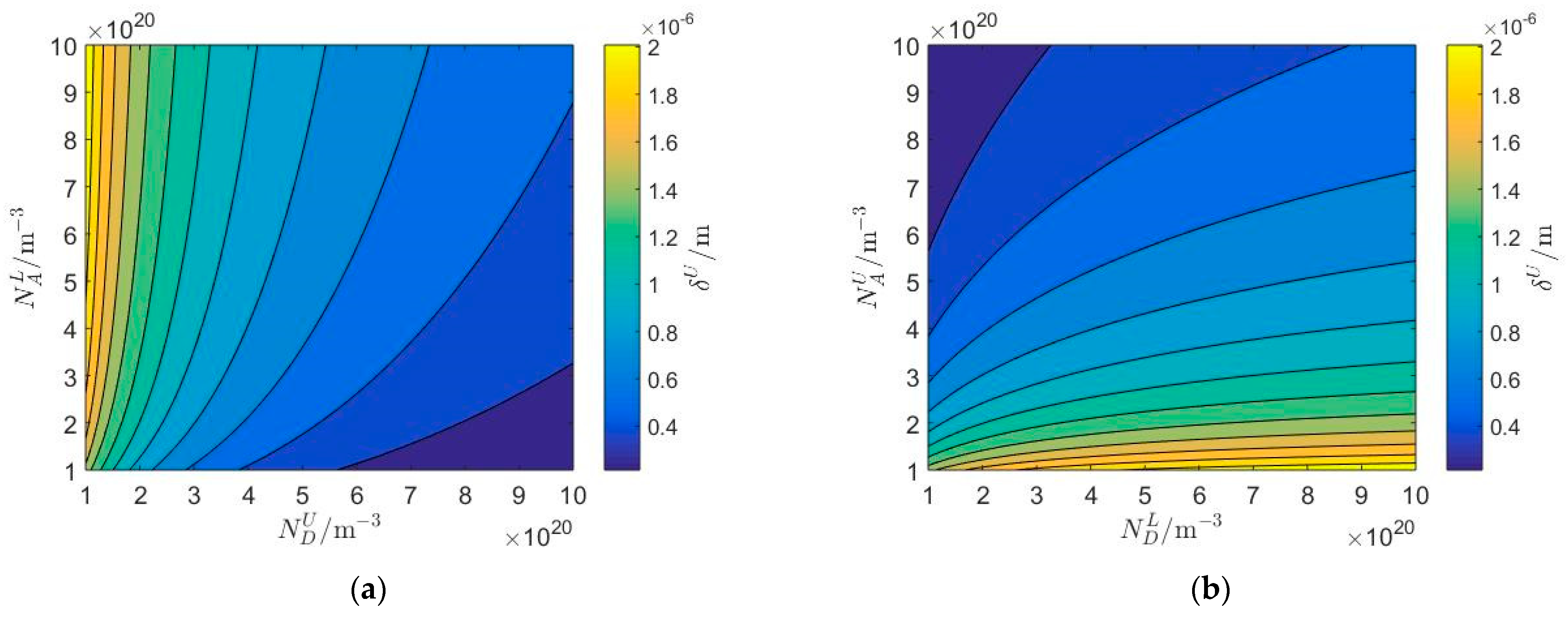
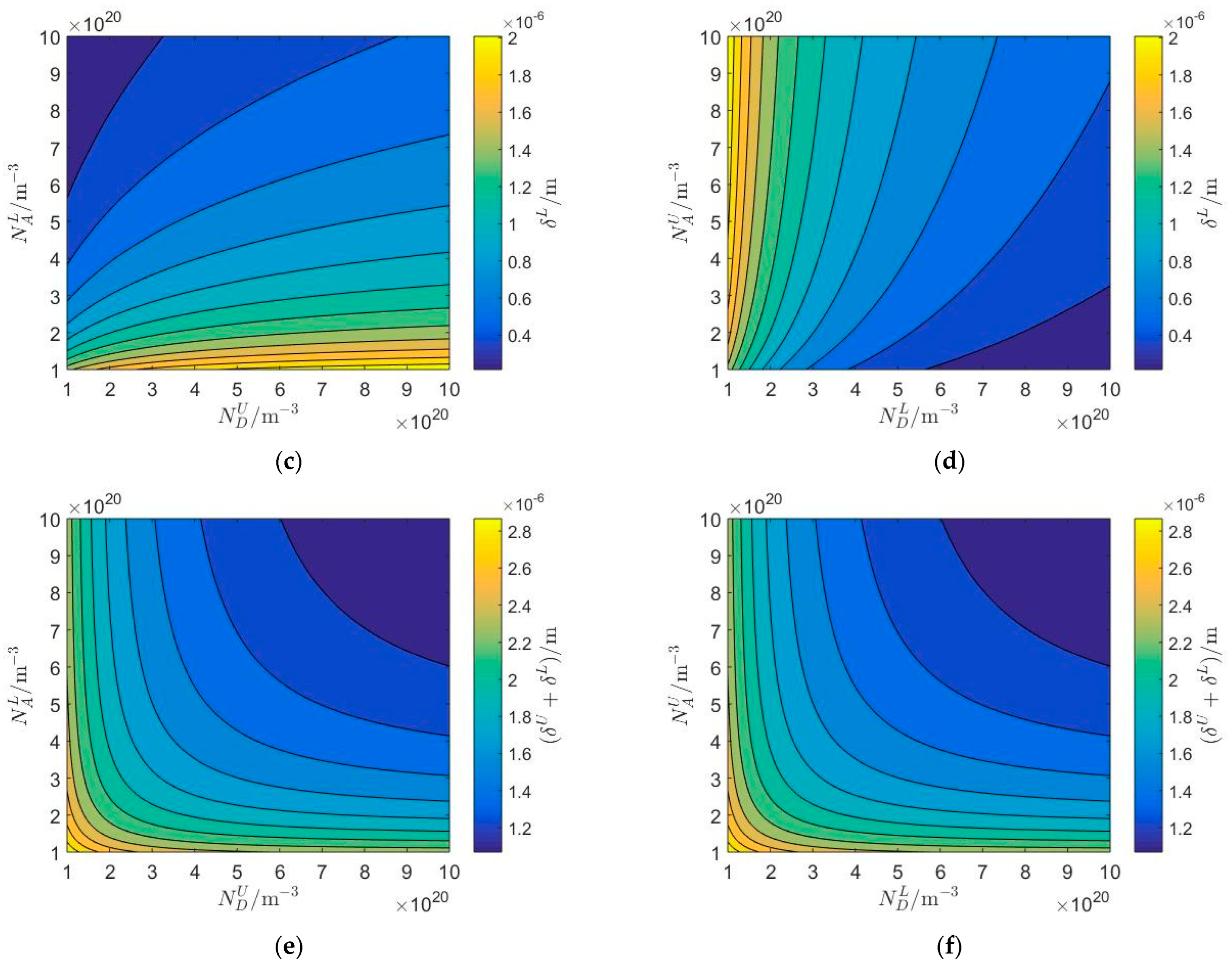
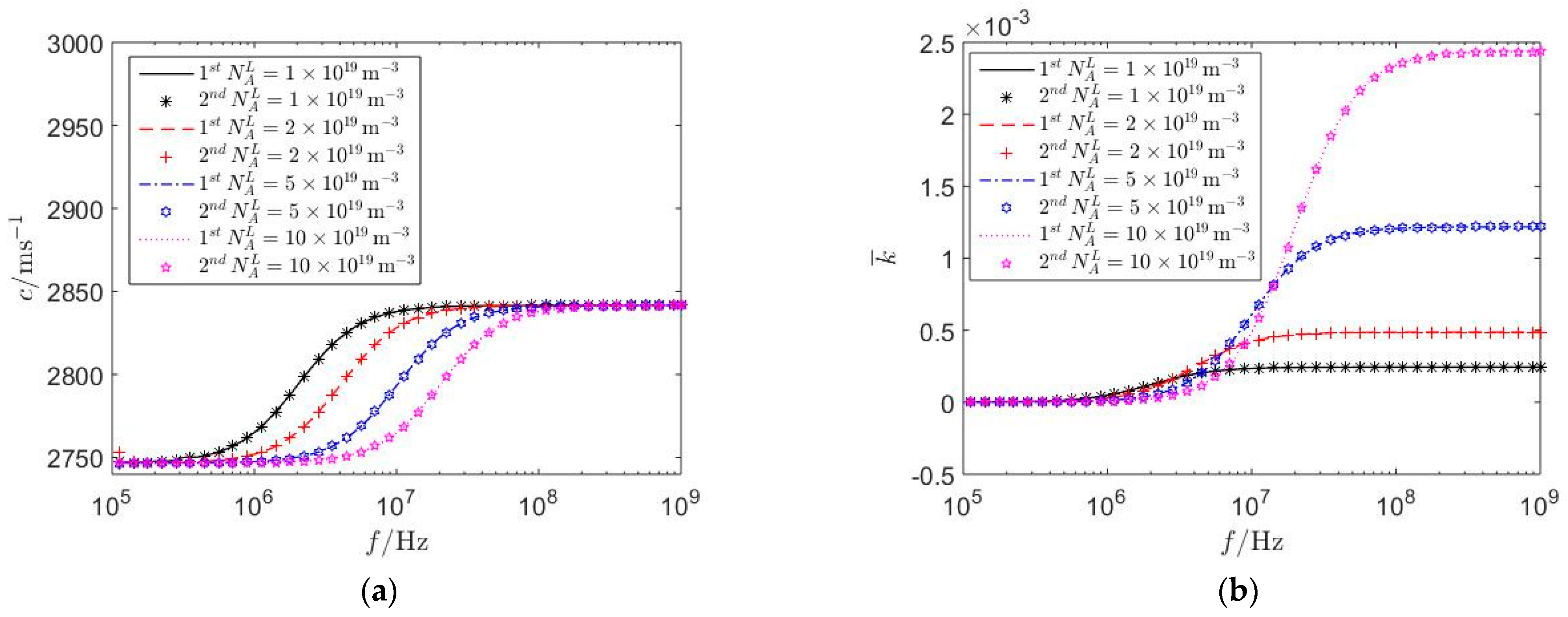
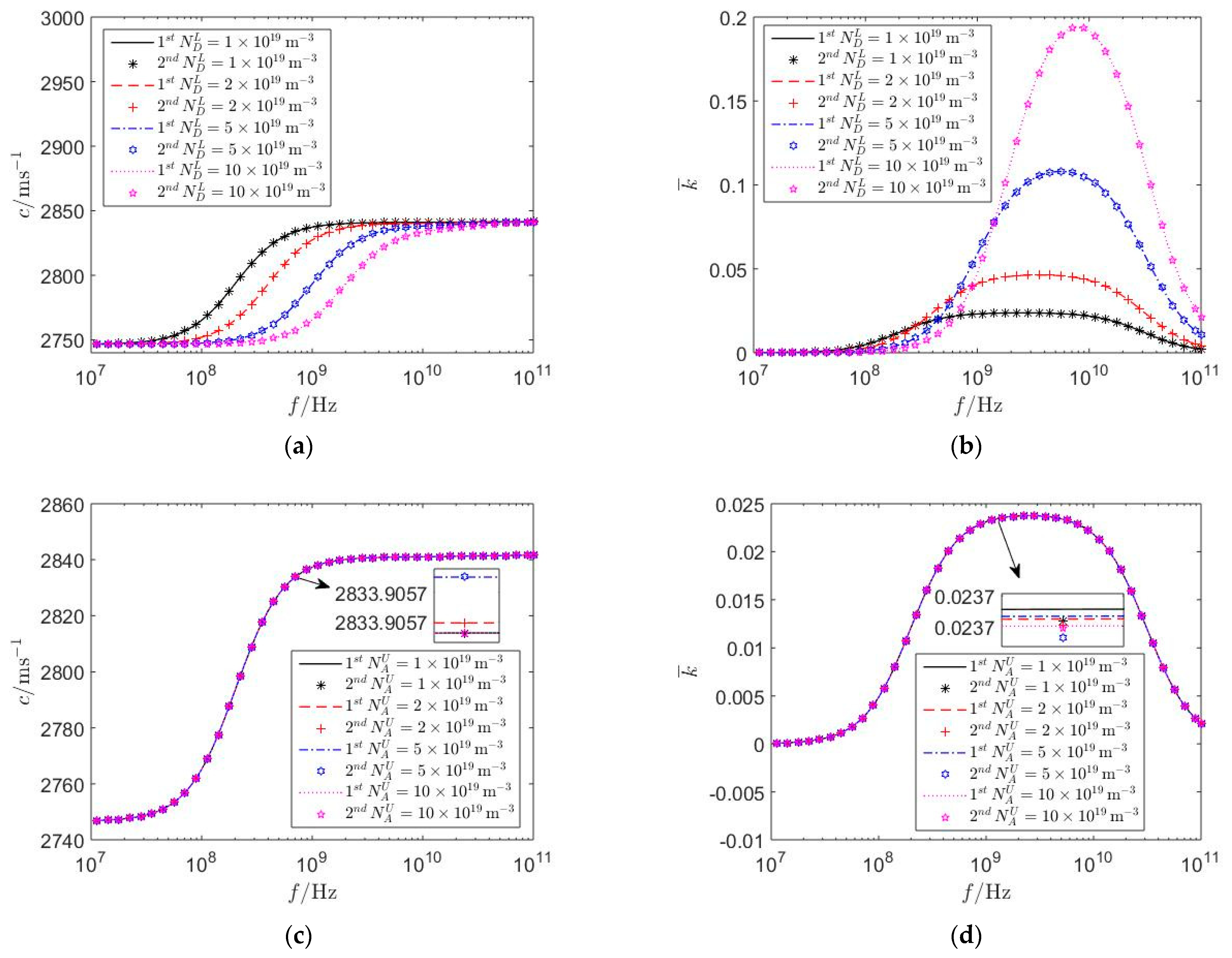
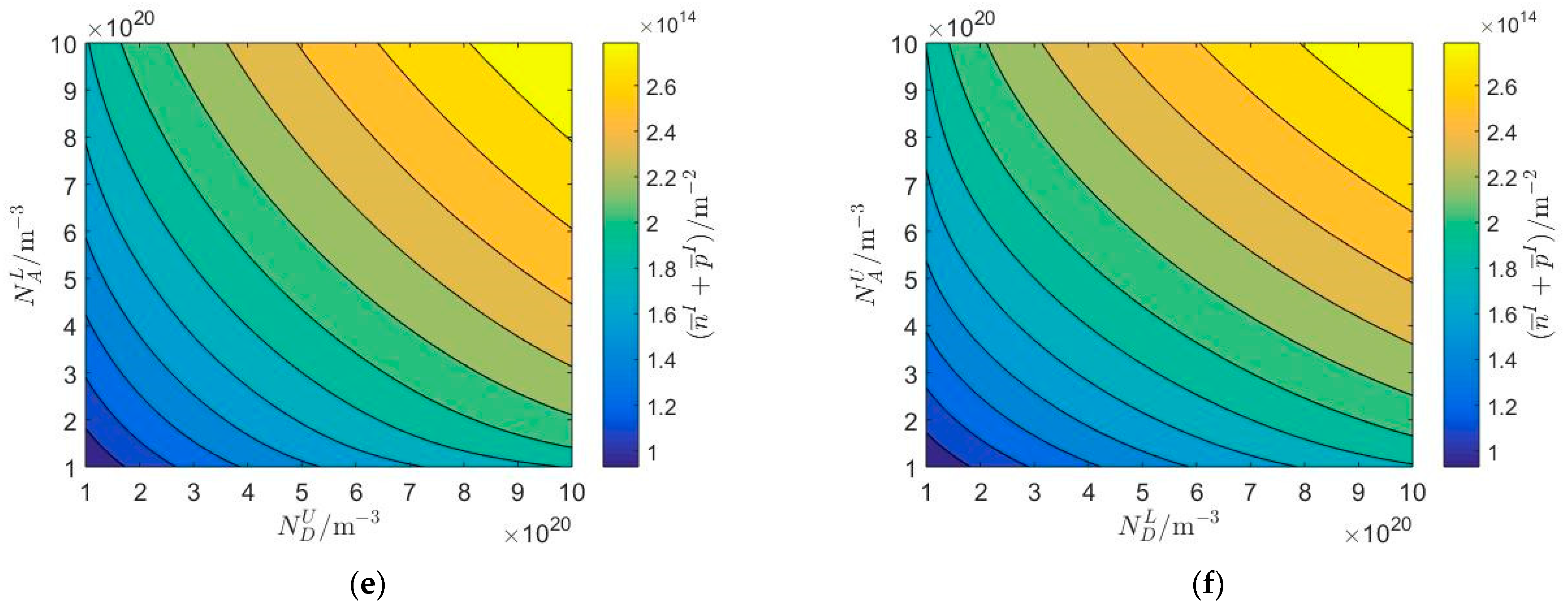
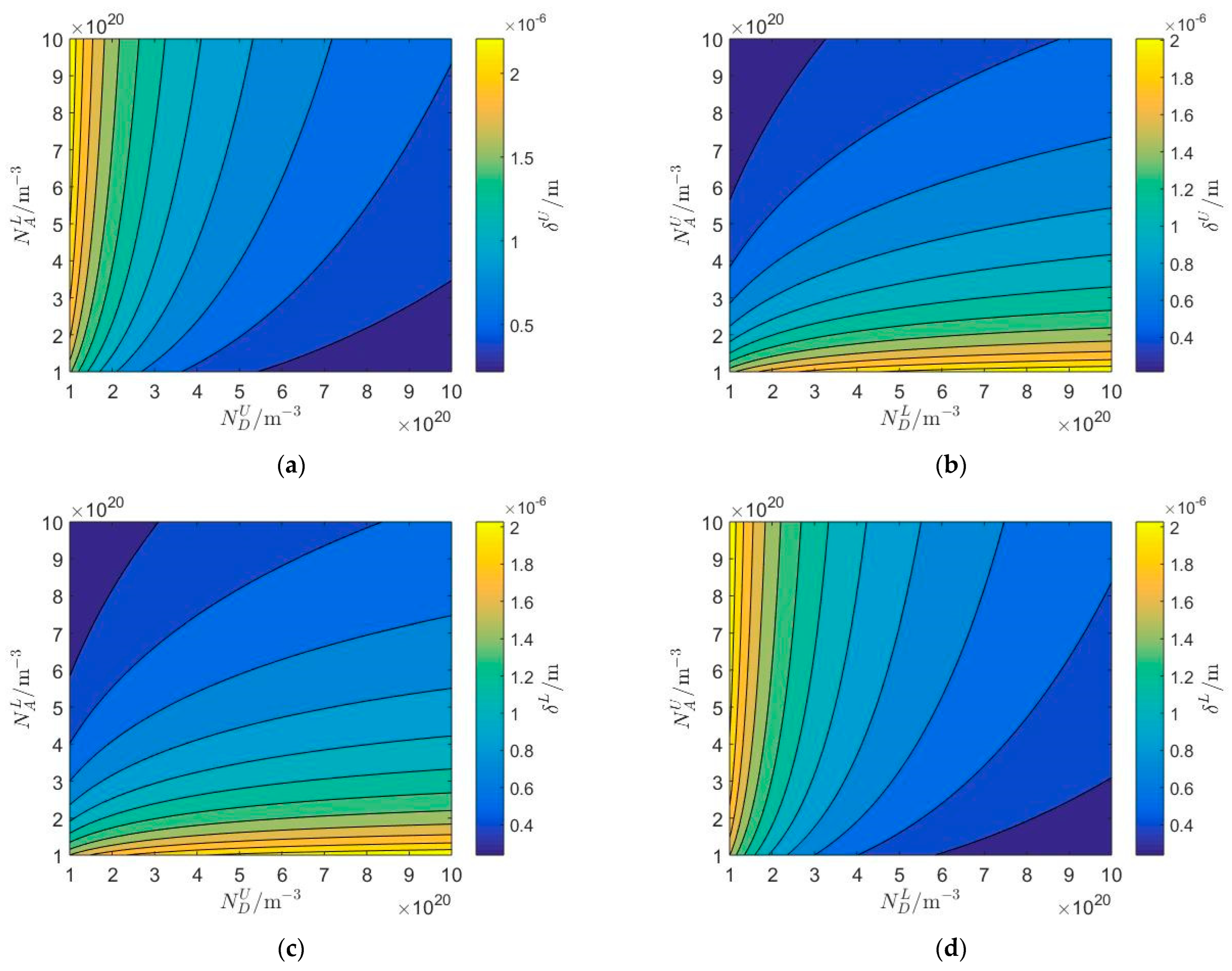
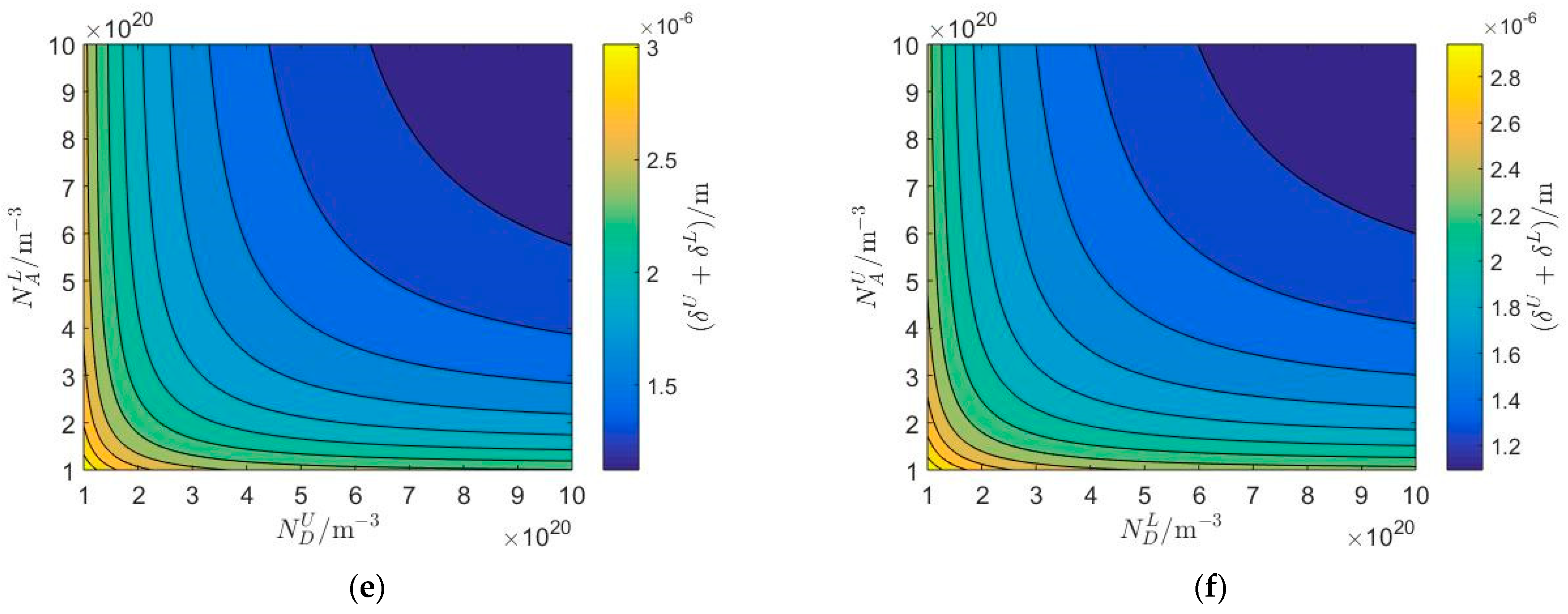
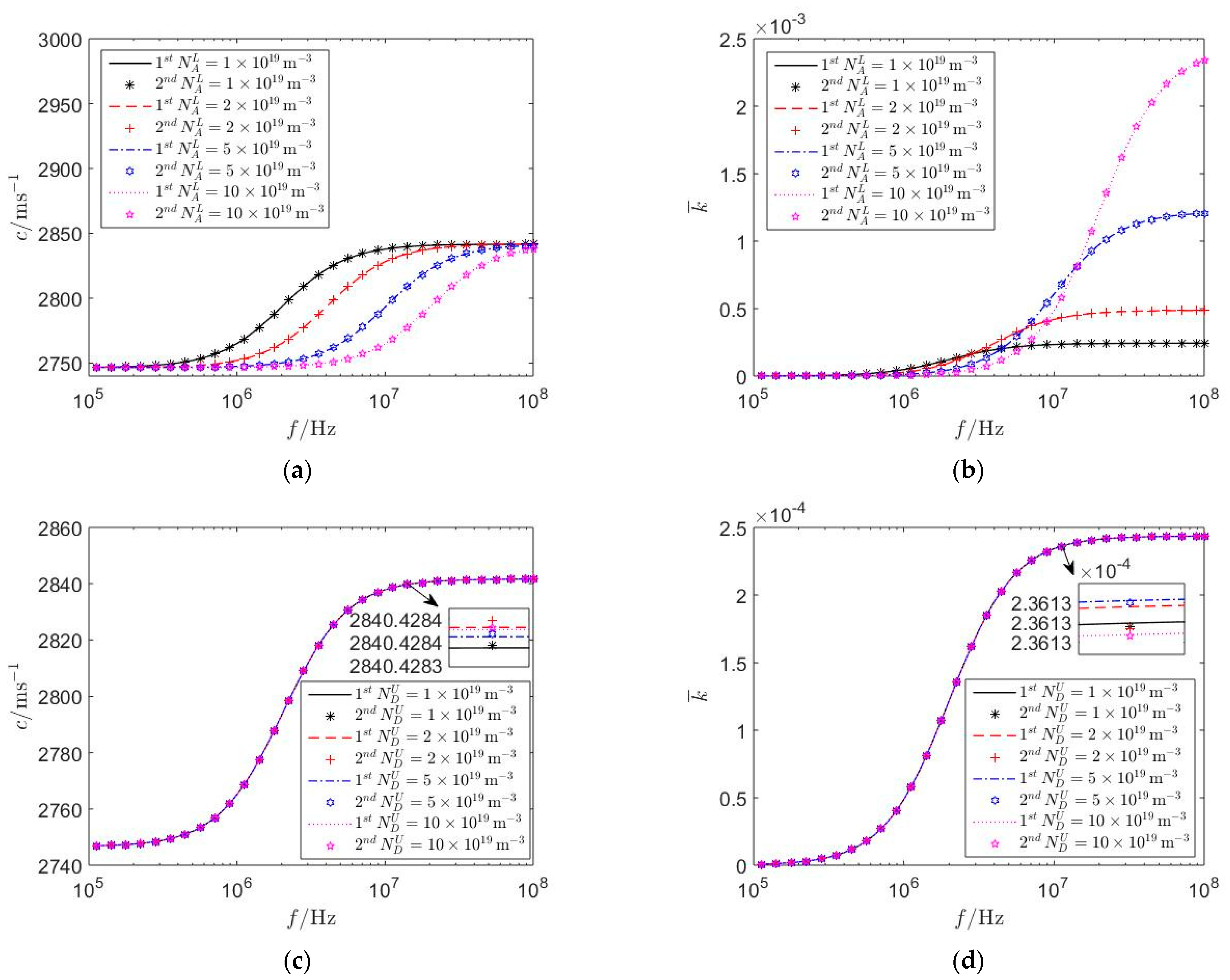
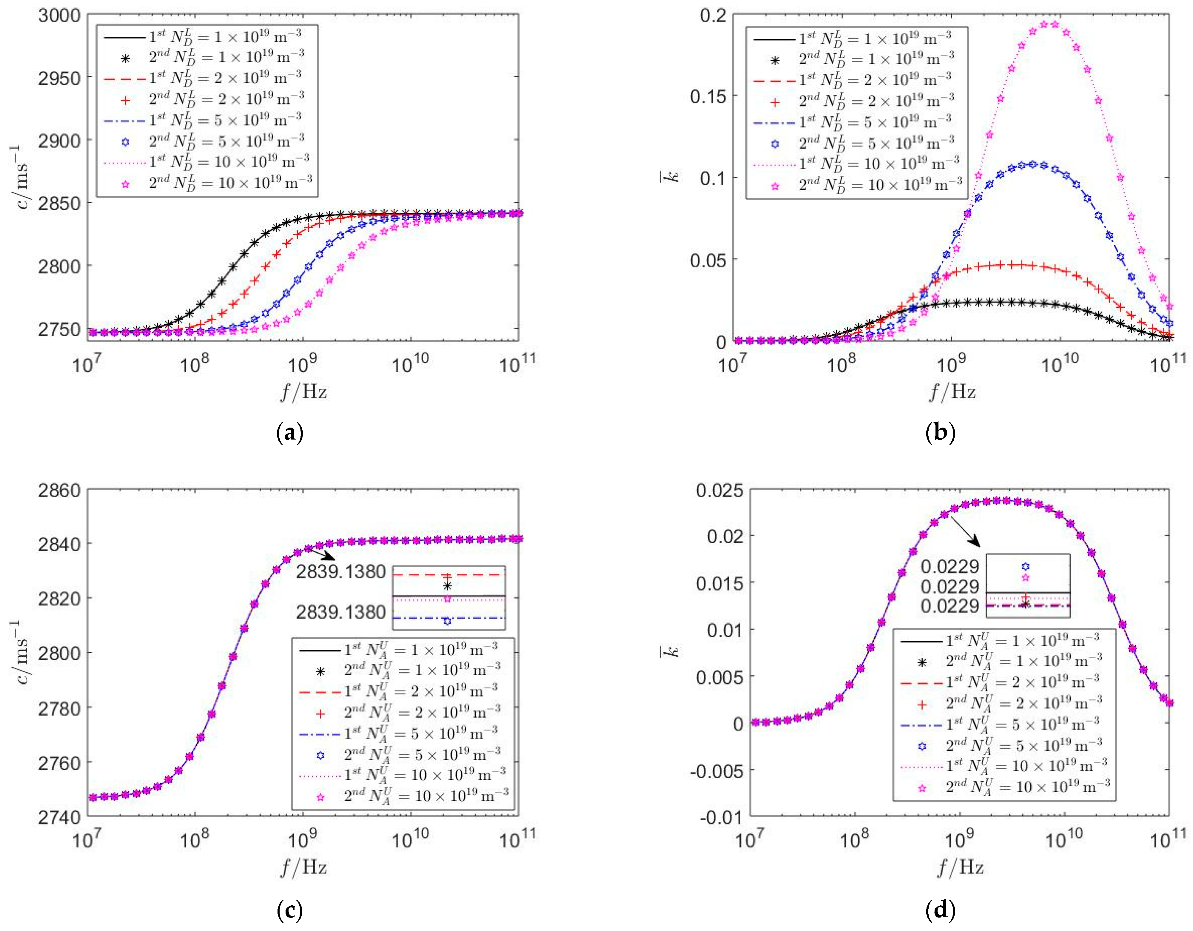
5.1. The Influence of Homo-Junctions

In this sub-section, the influence of the homo-junction on the dispersion and attenuation characteristics of Love waves, which appears in the PSC semi-infinite mediums for the combinations of upper n-type ZnO/lower p-type ZnO and upper p-type ZnO/lower n-type ZnO is systematically discussed. The thickness of the upper n-type or p-type ZnO layer is H = 10   μ m . Figure 2 and Figure 3 show the numerical distributions of steady electron and hole carrier concentrations and geometrical thicknesses of the depleted layers and homo-junction with the variation in the donor and acceptor concentrations. It is observed from Figure 2a–d that the numerical distribution of n ¯ I is dominated by the donor concentration in the upper n-type ZnO layer or lower n-type ZnO substrate, while the numerical distribution of p ¯ I is dominated by the acceptor concentration in the lower p-type ZnO substrate or upper p-type ZnO layer. With an increase in the donor and acceptor concentrations, the numerical values of n ¯ I and p ¯ I likewise increase. The mathematical reason for the above numerical results can be seen in Equations (33) and (34) that n ¯ I and p ¯ I are obtained by definite integrations with respect to c ¯ U and c ¯ L , which are dominated by the donor and acceptor concentrations in the upper ZnO layer and lower ZnO substrate, as shown in Equations (2) and (4). Since the upper layer and lower substrate are both ZnO, the numerical distributions of n ¯ I + p ¯ I in Figure 2e,f are approximately symmetrical with respect to the line N D U = N A L and N D L = N A U , respectively. It is further observed from Figure 3a–d that the numerical distribution of δ U is dominated by the donor or acceptor concentration in the upper ZnO layer, while the numerical distribution of δ L is dominated by the acceptor or donor concentration in the lower ZnO substrate. However, with an increase in the donor and acceptor concentrations, the numerical values of δ U and δ L likewise decrease, which means that an increase in the donor and acceptor concentrations brings the homo-junction closer to an interface. The mathematical reason for the above numerical results can be seen in Equations (3) and (5) that the donor or acceptor concentration in the upper ZnO layer and acceptor or donor concentration in the lower ZnO substrate is in the denominator of the mathematical expressions for δ U and δ L , respectively.
Figure 4 and Figure 5 show the influence of the homo-junction on the dispersion and attenuation curves of Love waves calculated by the first and second mathematical models without the consideration of biasing electric fields. The continuous curves are calculated using the first mathematical model, in which the numerical values of interface characteristic lengths are
f e U = f e L = 2.084982 × 10 3   m , f ε U = f ε L = 1.661900 × 10 3   m
for the combination of upper n-type ZnO/lower p-type ZnO and
f e U = f e L = 0.700 × 10 6   m , f ε U = f ε L = 0.700 × 10 6   m
for the combination of upper p-type ZnO/lower n-type ZnO. The discrete numerical points are calculated using the second mathematical model, which falls approximately on the continuous curves. It is observed that the variation in acceptor or donor concentration in the lower ZnO substrate has an evident influence on the dispersion and attenuation curves of Love waves, as shown in Figure 4a,b and Figure 5a,b, while the variation in the donor or acceptor concentration in the upper ZnO layer has negligible influence on the dispersion and attenuation curves of Love waves as shown in Figure 4c,d and Figure 5c,d. This means that the influence of the homo-junction on the dispersion and attenuation characteristics of Love waves mainly comes from the lower depleted layer in the lower ZnO substrate. When the frequencies of Love waves are low, the wave velocities of Love waves tend to a constant value, i.e., 2746   m / s , which is the wave velocity of the shear horizontal wave in the n-type or p-type ZnO material, and the dimensionless attenuation coefficients of Love waves tend to be 0 , which means that the attenuation characteristics of Love waves are not evident. With an increase in the frequency, the wave velocities of Love waves gradually increase and tend to another constant, i.e., 2841   m / s , and the dimensionless attenuation coefficients of Love waves also gradually increase and tend to positive constants, which is due to the influence of the homo-junction. Moreover, the higher the acceptor or donor concentration in the lower ZnO substrate, the larger the numerical value of the positive constant that the attenuation coefficient tends to be. This means that the existence of the homo-junction improves the attenuation characteristics of Love waves. It is found that the variation interval in the wave velocities and dimensionless attenuation coefficients of Love waves in Figure 4 is 1   MHz f 10   MHz approximately, of which the left and right endpoints are much lower than that in Figure 5, that is 0.1   GHz f 1   GHz approximately. The mathematical reason for the above numerical results can be seen in Table 1 that the numerical values of d y y L and μ y y L in the lower p-type ZnO substrate are much smaller than that in the lower n-type ZnO substrate, which means that the hole carriers in the lower p-type ZnO substrate can be regarded as heavy particles which are sensitive to low-frequency Love waves, while the electron carriers in the lower n-type ZnO substrate can be regarded as light particles which are sensitive to high-frequency Love waves. It is further found that the numerical values of interface characteristic lengths in Equation (50) are much higher than those in Equation (51). The mathematical reason for the above numerical results is that compared with the high-frequency Love waves, the apparent wave number components of low-frequency Love waves are much smaller, which means that the dimensionless attenuation coefficients of Love waves in Figure 4b,d are also much smaller than that in Figure 5b,d. Further combining Equation (35), it can be seen that the interface characteristic lengths corresponding to low-frequency Love waves must be higher than that of high-frequency Love waves. It is further observed from Figure 5d that the numerical values of dimensionless attenuation coefficients tend to 0 again when the frequency of the Love wave tends to 100   GHz . This is because the frequency of the Love wave gradually exceeds the sensitive frequency interval of the electron carriers in the lower n-type ZnO substrate, and the influence of the homo-junction gradually disappears.

5.2. The Influence of Hetero-Junctions

In this sub-section, the influence of the hetero-junction on the dispersion and attenuation characteristics of Love waves, which appears in the PSC semi-infinite mediums for the combinations of upper n-type Si/lower p-type ZnO and upper p-type Si/lower n-type ZnO is systematically discussed. The thickness of the upper n-type or p-type Si layer is also H = 10   μ m . Figure 6 and Figure 7 show the numerical distributions of steady electron and hole carrier concentrations and geometrical thicknesses of the depleted layers and hetero-junction with the variation in the donor and acceptor concentrations. Similar to the homo-junction, the numerical values of steady electron and hole carrier concentrations and geometrical thicknesses of hetero-junction are much smaller than that of the upper layer and lower substrate, which means that the hetero-junction can also be treated as an electrical imperfect interface.
Figure 8 and Figure 9 show the influence of the hetero-junction on the dispersion and attenuation curves of Love waves calculated by the first and second mathematical models without the consideration of biasing electric fields. The continuous curves and discrete numerical points are calculated using the first and second mathematical models, respectively. The numerical values of interface characteristic lengths are
f e U = 0   m , f e L = 40.814529 × 10 3   m ,
f ε U = 0.771989 × 10 3   m , f ε L = 1.027538 × 10 3   m
for the combination of upper n-type Si/lower p-type ZnO and
f e U = 0   m , f e L = 52.708 × 10 6   m ,
f ε U = 1952.631 × 10 6   m , f ε L = 1580.810 × 10 6   m
for the combination of upper p-type Si/lower n-type ZnO. Similar to the homo-junction, the discrete numerical points also fall approximately on the continuous curves regardless of the electrical open circuit or short circuit surface boundary conditions, which verifies the equivalence of the above two mathematical models and the effectiveness of the interface characteristic lengths. The variation interval in the wave velocities and dimensionless attenuation coefficients of Love waves in Figure 8 and Figure 9 is equal to that in Figure 4 and Figure 5, respectively, since the lower substrate is ZnO material. It is further observed that a limit of wave speed appears as the frequency of the Love wave gradually increases. This is because calculating the wave velocity and attenuation coefficient of Love waves is essentially an eigenvalues computation problem mathematically [26]. As the physical parameters of the intrinsic properties of the PSC materials, the wave speed and attenuation coefficient, which are closely related to the constitutive parameters of the PSC materials and independent of the excitation source, must have limit values. However, unlike the homo-junction, the numerical values of the four interface characteristic lengths in Equations (52) and (53) are not equal. The numerical values of the interface characteristic lengths concerning the hetero-junction are much higher than those with respect to the homo-junction. This is because the numerical values of the piezoelectric and dielectric parameters of Si and ZnO are different, and the carrier migration and diffusion parameters of the Si material are much larger than those of the ZnO material, as shown in Table 1. This means that when the Love wave propagates, the carrier migration and diffusion motion in the hetero-junction are more drastic, and the imperfect interface characteristics of the hetero-junction are stronger.

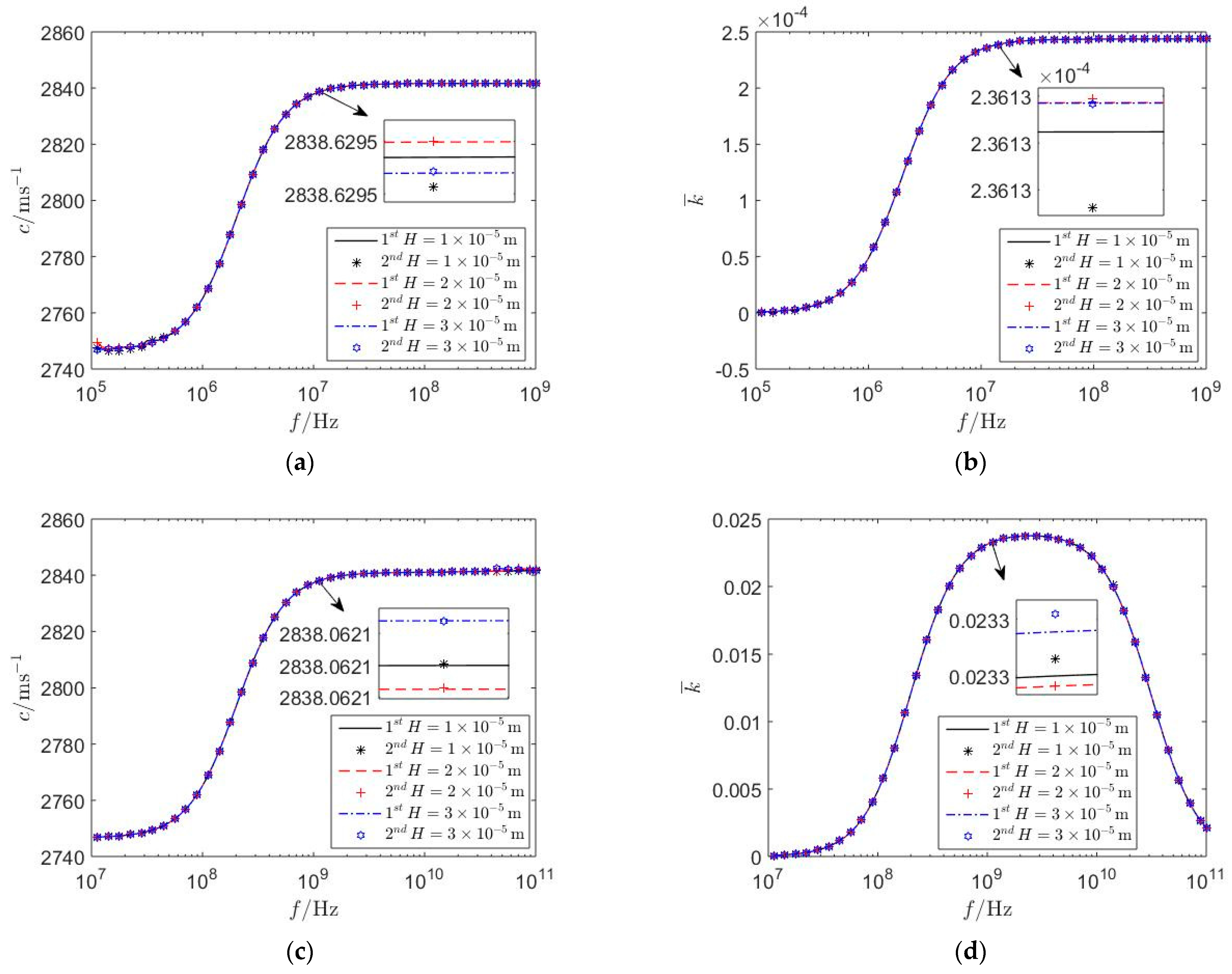
5.3. The Influence of the Thickness of the Upper PSC Layer and Biasing Electric Fields

In this sub-section, the influence of the thickness of the upper PSC layer and biasing electric fields on the dispersion and attenuation characteristics of Love waves is systematically discussed. The acceptor concentration in the upper n-type PSC layer or lower n-type PSC substrate is N A U = N A L = 1 × 10 19   m 3 and the donor concentration in the lower p-type PSC substrate or upper p-type PSC layer is also N D L = N D U = 1 × 10 19   m 3 . Figure 10 and Figure 11 show the dispersion and attenuation curves of Love waves with the variations in the thickness of the upper PSC layer and biasing electric fields, respectively. It is also observed that the discrete numerical points calculated using the second mathematical model fall approximately on the continuous curves using the first mathematical model regardless of the variations of H , E ¯ x , and E ¯ y , which further verifies the equivalence of the above two mathematical models and the effectiveness of the interface characteristic lengths. It is observed that the variations of H and E ¯ y have negligible influence on the dispersion and attenuation curves of Love waves, while the variation in E ¯ x has an evident influence on the dispersion and attenuation curves of Love waves. This is because the direction of E ¯ x is the same as the propagation direction of Love waves, as shown in Figure 1, which means that the dispersion and attenuation characteristics of Love waves can be modulated using the biasing electric field parallel to the PN junction. It is further observed from Figure 11b that the dimensionless attenuation coefficient of the Love wave gradually becomes negative with an increase in f when E ¯ x = 3 × 10 7   V / m , which implies that the wave motion energy of the Love wave no longer decays but gradually increases. This physical phenomenon is called the acoustoelectric amplification effect [32,33,34]; that is, the energy of the biasing electric field is converted into the wave motion energy of the Love wave due to the semiconductor effect, which can be utilized to design acoustoelectric, energy harvest and conversion devices [9,10,11,12].

6. Concluding Remarks

The influence of homo- and hetero-junctions on the dispersion and attenuation characteristics of Love waves in a PSC semi-infinite medium is the primary concern of the present work. According to the Gurtin–Murdoch theory [23,24,25], a new mathematical model of the interface effect originating from homo- and hetero-junctions is established through the spectral method [28,29,30,31], which includes four interface characteristic lengths to describe the electrical imperfect characteristics of homo- and hetero-junctions. To legitimately confirm these four interface characteristic lengths, another mathematical model is established, which is used to calculate the dispersion and attenuation curves of Love waves that can be compared. Based on numerical calculation results, the following conclusions can be drawn:
  • The electrical imperfect characteristics of homo- and hetero-junctions are closely related to the piezoelectric and semiconductor effect of the upper PSC layer and lower PSC substrate, while independent of the electrical surface boundary conditions, acceptor and donor concentrations, thickness of the upper PSC layer, and biasing electric fields in the PSC semi-infinite medium.
  • The variations of the type and combination of PSC materials can dramatically change the electrical imperfect characteristics of PN junctions, which might increase the complexity of the numerical values of interface characteristic lengths.
  • As the acceptor and donor concentrations and thickness of the upper PSC layer increase, homo- and hetero-junctions are closer to electrical imperfect interfaces, and the first mathematical model established in this paper is more applicable, which provides a theoretical basis for the investigation of the propagation surface acoustic waves in PSC materials.
Since the high-frequency and short-wavelength Love wave is an important class of surface acoustic waves propagating in micro- and nano-scale PSC materials, the establishment of mathematical models and the revelation of physical mechanisms are fundamental to information communication, energy conversion, and nondestructive testing technologies [9,10,11,12]. Since only a single PN is considered in the mathematical models established in this paper, the influence of homo- or hetero-junction on the dispersion and attenuation characteristics of Love waves is not evident in the case of some doping concentrations, as shown in Figure 4c,d, Figure 5c,d, Figure 8c,d and Figure 9c,d. Therefore, we might consider the influence of multi-layer PN junctions on the dispersion and attenuation characteristics of high-frequency and short-wavelength Love waves in more complex PSC materials in subsequent work through the mathematical models established in this paper.

Author Contributions

Conceptualization, X.G.; methodology, X.G.; software, X.G.; validation, X.G.; formal analysis, Y.W.; investigation, Y.W.; resources, C.X.; data curation, C.X.; writing—original draft preparation, Z.W.; writing—review and editing, Z.W.; visualization, C.D.; supervision, C.D.; All authors have read and agreed to the published version of the manuscript.

Funding

The whole research is supported by the National Natural Science Foundation of China (12202039) and the Interdisciplinary Research Project for Young Teachers of USTB (Fundamental Research Funds for the Central Universities) (FRF-IDRY-21-006).

Data Availability Statement

The data that support the findings of this study are available upon request from the corresponding author, Xiao Guo ([email protected]), upon reasonable request.

Conflicts of Interest

The authors declare that they have no conflicts of interest in this work. The authors declare that they do not have any commercial or associative interest that represents a conflict of interest in connection with the work submitted.

Appendix A

The explicit expressions of coefficient matrices A ¯ , B ¯ , C ¯ , and D ¯ in Equation (38) are
A ¯ = [ A ¯ j m 1 , 1 A ¯ j m 1 , 2 O O O O A ¯ j m 2 , 1 A ¯ j m 2 , 2 O O O O O A ¯ j m 3 , 2 A ¯ j m 3 , 3 O O O O O O A ¯ j m 4 , 4 A ¯ j m 4 , 5 O O O O A ¯ j m 5 , 4 A ¯ j m 5 , 5 O O O O O A ¯ j m 6 , 5 A ¯ j m 6 , 6 ] ,  
B ¯ = [ O O O O O O O O O O O O O O B ¯ j m 3 , 3 O O O O O O O O O O O O O O O O O O O O B ¯ j m 6 , 6 ] ,
D ¯ = [ D ¯ j m 1 , 1 O O O O O O O O O O O O O D ¯ j m 3 , 3 O O O O O O D ¯ j m 4 , 4 O O O O O O O O O O O O O D ¯ j m 6 , 6 ]
where
A ¯ j m 1 , 1 = c y z y z U 0 H R m U ( y ) R j U ( y ) d y ,
A ¯ j m 1 , 2 = e y y z U 0 H R m U ( y ) R j U ( y ) d y ,
A ¯ j m 2 , 1 = e y y z U 0 H R m U ( y ) R j U ( y ) d y ,
A ¯ j m 2 , 2 = ε y y U 0 H R m U ( y ) R j U ( y ) d y ,
A ¯ j m 3 , 3 = α U d y y U 0 H R m U ( y ) R j U ( y ) d y ,
A ¯ j m 4 , 4 = c y z y z L 0 R m L ( y ) R j L ( y ) d y ,
A ¯ j m 4 , 5 = e y y z L 0 R m L ( y ) R j L ( y ) d y ,
A ¯ j m 5 , 4 = e y y z L 0 R m L ( y ) R j L ( y ) d y + ( f e U e x x z U + f e L e x x z L ) R m L ( 0 ) R j L ( 0 ) ,
A ¯ j m 5 , 5 = ε y y L 0 R m L ( y ) R j L ( y ) d y ( f ε U ε x x U + f ε L ε x x L ) R m L ( 0 ) R j L ( 0 ) ,
A ¯ j m 6 , 6 = α L d y y L 0 R m L ( y ) R j L ( y ) d y + ( α L d x x L δ L + α U d x x U δ U ) R m L ( 0 ) R j L ( 0 ) ,
B ¯ j m 3 , 3 = i μ y y U E ¯ x 0 H R m U ( y ) R j U ( y ) d y ,
B ¯ j m 6 , 6 = i μ y y L E ¯ x 0 R m L ( y ) R j L ( y ) d y i ( μ x x L δ L + μ x x U δ U ) E ¯ x R m L ( 0 ) R j L ( 0 ) ,
D ¯ j m 1 , 1 = ρ U ω 2 0 H R m U ( y ) R j U ( y ) d y ,
D ¯ j m 3 , 3 = α U i ω 0 H R m U ( y ) R j U ( y ) d y ,
D ¯ j m 4 , 4 = ρ L ω 2 0 R m L ( y ) R j L ( y ) d y ,
D ¯ j m 6 , 6 = α L i ω 0 R m L ( y ) R j L ( y ) d y ,
0 H R m U ( y ) R j U ( y ) d y = H 2 m + 1 δ m , j ,
δ m , j = { 0 m j 1 m = j ,
0 R m L ( y ) R j L ( y ) d y = δ m , j ,
R m L ( 0 ) = 1
and
A ¯ j m 3 , 2 = μ y y U N D U 0 H R m U ( y ) R j U ( y ) d y ,
A ¯ j m 6 , 5 = μ y y L N A L 0 R m L ( y ) R j L ( y ) d y ( p ¯ I μ x x L + n ¯ I μ x x U ) R m L ( 0 ) R j L ( 0 )
for the combination of upper n-type PSC layer and lower p-type PSC substrate,
A ¯ j m 3 , 2 = μ y y U N A U 0 H R m U ( y ) R j U ( y ) d y ,
A ¯ j m 6 , 5 = μ y y L N D L 0 R m L ( y ) R j L ( y ) d y ( p ¯ I μ x x U + n ¯ I μ x x L ) R m L ( 0 ) R j L ( 0 )
for the combination of the upper p-type PSC layer and lower n-type PSC substrate. For the case of the mechanical open circuit electrical open circuit surface boundary condition, the explicit expression of the coefficient matrix C ¯ in Equation (38) is
C ¯ = C ¯ j m 1,1 , 1 C ¯ j m 1,1 , 2 O C ¯ j m 1,4 C ¯ j m 1,5 O C ¯ j m 1,2 , 1 C ¯ j m 1,2 , 2 C ¯ j m 1,2 , 3 C ¯ j m 2,4 C ¯ j m 2,5 O O C ¯ j m 1,3 , 2 C ¯ j m 1,3 , 3 O C ¯ j m 3,5 C ¯ j m 3,6 C ¯ j m 4,1 C ¯ j m 4,2 O C ¯ j m 4,4 C ¯ j m 4,5 O C ¯ j m 5,1 C ¯ j m 5,2 O C ¯ j m 5,4 C ¯ j m 5,5 C ¯ j m 5,6 O C ¯ j m 6,2 C ¯ j m 6,3 O C ¯ j m 6,5 C ¯ j m 6,6
where
C ¯ j m 1 , 1 , 1 = c y z y z U ( R m U ( 0 ) R j U ( 0 ) R m U ( H ) R j U ( H ) + 0 H R m U ( y ) R j U ( y ) d y ) ,
C ¯ j m 1 , 1 , 2 = e y y z U ( R m U ( 0 ) R j U ( 0 ) R m U ( H ) R j U ( H ) + 0 H R m U ( y ) R j U ( y ) d y ) ,
C ¯ j m 1 , 4 = c y z y z U R m L ( 0 ) R j U ( 0 ) ,
C ¯ j m 1 , 5 = e y y z U R m L ( 0 ) R j U ( 0 ) ,
C ¯ j m 1 , 2 , 1 = e y y z U ( R m U ( 0 ) R j U ( 0 ) R m U ( H ) R j U ( H ) + 0 H R m U ( y ) R j U ( y ) d y ) ,
C ¯ j m 1 , 2 , 2 = ε y y U ( R m U ( 0 ) R j U ( 0 ) R m U ( H ) R j U ( H ) + 0 H R m U ( y ) R j U ( y ) d y ) ,
C ¯ j m 1 , 2 , 3 = α U q 0 H R m U ( y ) R j U ( y ) d y ,
C ¯ j m 2 , 4 = e y y z U R m L ( 0 ) R j U ( 0 ) , C ¯ j m 2 , 5 = ε y y U R m L ( 0 ) R j U ( 0 ) ,
C ¯ j m 1 , 3 , 3 = μ y y U E ¯ y ( R m U ( 0 ) R j U ( 0 ) 0 H R m U ( y ) R j U ( y ) d y ) + α U d y y U ( R m U ( 0 ) R j U ( 0 ) R m U ( H ) R j U ( H ) + 0 H R m U ( y ) R j U ( y ) d y ) ,
C ¯ j m 3 , 6 = α U d y y U R m L ( 0 ) R j U ( 0 ) ,
C ¯ j m 4 , 1 = c y z y z U R m U ( 0 ) R j L ( 0 ) ( 0 ) ,
C ¯ j m 4 , 2 = e y y z U R m U ( 0 ) R j L ( 0 ) ,
C ¯ j m 4 , 4 = c y z y z L 0 R m L ( y ) R j L ( y ) d y ,
C ¯ j m 4 , 5 = e y y z L 0 R m L ( y ) R j L ( y ) d y ,
C ¯ j m 5 , 1 = e y y z U R m U ( 0 ) R j L ( 0 ) ,
C ¯ j m 5 , 2 = ε y y U R m U ( 0 ) R j L ( 0 ) ,
C ¯ j m 5 , 4 = k 2 ( f e U e x x z U + f e L e x x z L ) R m L ( 0 ) R j L ( 0 ) e y y z L 0 R m L ( y ) R j L ( y ) d y ,
C ¯ j m 5 , 5 = k 2 ( f ε U ε x x U + f ε L ε x x L ) R m L ( 0 ) R j L ( 0 ) + ε y y L 0 R m L ( y ) R j L ( y ) d y ,
C ¯ j m 5 , 6 = α L q 0 R m L ( y ) R j L ( y ) d y ,
C ¯ j m 6 , 3 = μ y y U E ¯ y R m U ( 0 ) R j L ( 0 ) + α U d y y U R m U ( 0 ) R j L ( 0 ) , C ¯ j m 6,6 = μ y y L E ¯ y 0 R m L y R j L y d y + α L d y y L 0 R m L y R j L y d y ,
R m U ( H ) = 1 , R m U ( H ) = m ( m + 1 ) H ,
R m U ( 0 ) = ( 1 ) m ,
R m U ( 0 ) = ( 1 ) m + 1 m ( m + 1 ) H ,
0 H R m U ( y ) R j U ( y ) d y = { l = 0 n 2 δ 2 l 1 , m j = 2 n l = 0 n 2 δ 2 l , m j = 2 n + 1 ,
0 H R m U ( y ) R j U ( y ) d y = 2 j j + 1 H 2 min j , m · m i n j , m + 1 H j + m 0   m o d   2 0 j + m 1   m o d   2 ,
R m L ( 0 ) = 1 2 + m ,
0 R j L ( y ) R m L ( y ) d y = 1 2 δ j , m + h 1 ( j m 1 ) ,
0 R j L ( y ) R m L ( y ) d y = 1 4 δ j , m + ( j m ) h 1 ( j m 1 ) ,
h 1 ( y ) = { 0 y < 0 1 y 0
and
C ¯ j m 1 , 3 , 2 = N D U μ y y U ( R m U ( 0 ) R j U ( 0 ) R m U ( H ) R j U ( H ) + 0 H R m U ( y ) R j U ( y ) d y ) ,
C ¯ j m 3 , 5 = N D U μ y y U R m L ( 0 ) R j U ( 0 ) ,
C ¯ j m 6 , 2 = μ y y U N D U R m U ( 0 ) R j L ( 0 ) ,
C ¯ j m 6 , 5 = μ y y L N A L 0 R m L ( y ) R j L ( y ) d y
for the combination of upper n-type PSC layer and lower p-type PSC substrate and
C ¯ j m 1 , 3 , 2 = N A U μ y y U ( R m U ( 0 ) R j U ( 0 ) R m U ( H ) R j U ( H ) + 0 H R m U ( y ) R j U ( y ) d y ) ,
C ¯ j m 3 , 5 = N A U μ y y U R m L ( 0 ) R j U ( 0 ) ,
C ¯ j m 6 , 2 = μ y y U N A U R m U ( 0 ) R j L ( 0 ) ,
C ¯ j m 6 , 5 = μ y y L N D L 0 R m L ( y ) R j L ( y ) d y
for the combination of the upper p-type PSC layer and lower n-type PSC substrate. For the case of the mechanical open circuit electrical short circuit surface boundary condition, the explicit expression of the coefficient matrix C ¯ in Equation (38) is
C ¯ = C ¯ j m 2,1 , 1 C ¯ j m 2,1 , 2 O C ¯ j m 1,4 C ¯ j m 1,5 O C ¯ j m 2,2 , 1 C ¯ j m 2,2 , 2 C ¯ j m 2,2 , 3 O C ¯ j m 2,5 O O C ¯ j m 2,3 , 2 C ¯ j m 2,3 , 3 O C ¯ j m 3,5 C ¯ j m 3,6 C ¯ j m 4,1 C ¯ j m 4,2 O C ¯ j m 4,4 C ¯ j m 4,5 O C ¯ j m 5,1 C ¯ j m 5,2 O C ¯ j m 5,4 C ¯ j m 5,5 C ¯ j m 5,6 O C ¯ j m 6,2 C ¯ j m 6,3 O C ¯ j m 6,5 C ¯ j m 6,6
where
C ¯ j m 2 , 1 , 1 = C ¯ j m 1 , 1 , 1 ,
C ¯ j m 2 , 1 , 2 = C ¯ j m 1 , 1 , 2 ,
C ¯ j m 2 , 2 , 1 = e y y z U 0 H R m U ( y ) R j U ( y ) d y ,
C ¯ j m 2 , 2 , 2 = ε y y U ( R m U ( H ) R j U ( H ) R m U ( 0 ) R j U ( 0 ) + 0 H R m U ( y ) R j U ( y ) d y ) , C ¯ j m 2 , 2 , 3 = C ¯ j m 1 , 2 , 3 ,
C ¯ j m 2,3 , 3 = μ y y U E ¯ y 0 H R m U y R j U y d y + d y y U ( R m U ( H ) R j U ( H ) R m U ( 0 ) R j U ( 0 ) + 0 H R m U ( y ) R j U ( y ) d y )
and
C ¯ j m 2 , 3 , 2 = μ y y U N D U ( R m U ( H ) R j U ( H ) R m U ( 0 ) R j U ( 0 ) + 0 H R m U ( y ) R j U ( y ) d y )
for the combination of upper n-type PSC layer and lower p-type PSC substrate and
C ¯ j m 2 , 3 , 2 = μ y y U N A U ( R m U ( H ) R j U ( H ) R m U ( 0 ) R j U ( 0 ) + 0 H R m U ( y ) R j U ( y ) d y )
for the combination of the upper p-type PSC layer and lower n-type PSC substrate.
The explicit expressions of coefficient matrices A , B , and D in Equation (48) are
A = [ A j m 1 , 1 A j m 1 , 2 O O O O A j m 2 , 1 A j m 2 , 2 O O O O O A j m 3 , 2 A j m 3 , 3 O O O O O O A j m 4 , 4 A j m 4 , 5 O O O O A j m 5 , 4 A j m 5 , 5 O O O O O A j m 6 , 5 A j m 6 , 6 ] ,
B = [ O O O O O O O O O O O O O O B j m 3 , 3 O O O O O O O O O O O O O O O O O O O O B j m 6 , 6 ] ,
D = [ D j m 1 , 1 O O O O O O O O O O O O O D j m 3 , 3 O O O O O O D j m 4 , 4 O O O O O O O O O O O O O D j m 6 , 6 ] ,
where
A j m 1 , 1 = A ¯ j m 1 , 1 ,
A j m 1 , 2 = A ¯ j m 1 , 2 ,
A j m 2 , 1 = A ¯ j m 2 , 1 ,
A j m 2 , 2 = A ¯ j m 2 , 2 ,
A j m 3 , 2 = μ y y U 0 H c ¯ U ( y ) R m U ( y ) R j U ( y ) d y ,
A j m 3 , 3 = A ¯ j m 3 , 3 ,
A j m 4 , 4 = A ¯ j m 4 , 4 ,
A j m 4 , 5 = A ¯ j m 4 , 5 ,
A j m 5 , 4 = e y y z L 0 R m L ( y ) R j L ( y ) d y ,
A j m 5 , 5 = α L d y y L 0 R m L ( y ) R j L ( y ) d y ,
A j m 6 , 5 = μ y y L 0 c ¯ L ( y ) R m L ( y ) R j L ( y ) d y ,
A j m 6 , 6 = α L d y y L 0 R m L ( y ) R j L ( y ) d y ,
B j m 3 , 3 = B ¯ j m 3 , 3 ,
B j m 6 , 6 = i μ y y L E ¯ x 0 R m L ( y ) R j L ( y ) d y ,
D j m 1 , 1 = D ¯ j m 1 , 1 ,
D j m 3 , 3 = D ¯ j m 3 , 3 ,
D j m 4 , 4 = D ¯ j m 4 , 4 ,
D j m 6 , 6 = D ¯ j m 6 , 6 .
For the case of the mechanical open circuit electrical open circuit surface boundary condition, the explicit expression of coefficient matrix C in Equation (48) is
C = C j m 1,1 , 1 C j m 1,1 , 2 O C j m 1,4 C j m 1,5 O C j m 1,2 , 1 C j m 1,2 , 2 C j m 1,2 , 3 C j m 2,4 C j m 2,5 O O C j m 1,3 , 2 C j m 1,3 , 3 O O C j m 3,6 C j m 4,1 C j m 4,2 O C j m 4,4 C j m 4,5 O C j m 5,1 C j m 5,2 O C j m 5,4 C j m 5,5 C j m 5,6 O C j m 6,2 C j m 6,3 O C j m 6,5 C j m 6,6
where
C j m 1 , 1 , 1 = C ¯ j m 1 , 1 , 1 ,
C j m 1 , 1 , 2 = C ¯ j m 1 , 1 , 2 ,
C j m 1 , 2 , 3 = C ¯ j m 1 , 2 , 3 ,
C j m 1 , 4 = C ¯ j m 1 , 4 ,
C ¯ j m 1 , 5 = C j m 1 , 5 ,
C j m 1 , 2 , 1 = C ¯ j m 1 , 2 , 1 ,
C j m 1 , 2 , 2 = C ¯ j m 1 , 2 , 2 ,
C j m 2 , 4 = C ¯ j m 2 , 4 ,
C j m 2 , 5 = C ¯ j m 2 , 5 ,
C j m 1 , 3 , 2 = μ y y U ( c ¯ U ( 0 ) R m U ( 0 ) R j U ( 0 ) 0 H c ¯ U ( y ) R m U ( y ) R j U ( y ) d y ) ,
C j m 1 , 3 , 3 = C ¯ j m 1 , 3 , 3 ,
C j m 3 , 6 = C ¯ j m 3 , 6 ,
C j m 4 , 1 = C ¯ j m 4 , 1 ,
C j m 4 , 2 = C ¯ j m 4 , 2 ,
C j m 4 , 4 = C ¯ j m 4 , 4 ,
C j m 4 , 5 = C ¯ j m 4 , 5 ,
C j m 5 , 1 = C ¯ j m 5 , 1 ,
C j m 5 , 2 = C ¯ j m 5 , 2 ,
C j m 5 , 4 = e y y z L 0 R m L ( y ) R j L ( y ) d y ,
C j m 5 , 5 = ε y y L 0 R m L ( y ) R j L ( y ) d y ,
C j m 5 , 6 = C ¯ j m 5 , 6 ,
C j m 6 , 2 = μ y y U c ¯ U ( 0 ) R m U ( 0 ) R j L ( 0 ) ,
C j m 6 , 3 = C ¯ j m 6 , 3 , C j m 6,5 = μ y y L 0 c ¯ L y R m L y R j L y d y ,
C j m 6 , 6 = C ¯ j m 6 , 6
For the case of the mechanical open circuit electrical short circuit surface boundary condition, the explicit expression of coefficient matrix C in Equation (48) is
C = [ C j m 2 , 1 , 1 C j m 2 , 1 , 2 O C j m 1 , 4 C j m 1 , 5 O C j m 2 , 2 , 1 C j m 2 , 2 , 2 C j m 2 , 2 , 3 O C j m 2 , 5 O O C j m 2 , 3 , 2 C j m 2 , 3 , 3 O O C j m 3 , 6 C j m 4 , 1 C j m 4 , 2 O C j m 4 , 4 C j m 4 , 5 O C j m 5 , 1 C j m 5 , 2 O C j m 5 , 4 C j m 5 , 5 C j m 5 , 6 O C j m 6 , 2 C j m 6 , 3 O C j m 6 , 5 C j m 6 , 6 ]
where
C j m 2 , 1 , 1 = C ¯ j m 2 , 1 , 1 ,
C j m 2 , 1 , 2 = C ¯ j m 2 , 1 , 2 ,
C j m 2 , 2 , 1 = C ¯ j m 2 , 2 , 1 ,
C j m 2 , 2 , 2 = C ¯ j m 2 , 2 , 2 ,
C j m 2 , 2 , 3 = C ¯ j m 2 , 2 , 3 ,
C j m 2 , 3 , 2 = μ y y U 0 H ( c ¯ U ( y ) R m U ( y ) + c ¯ U ( y ) R m U ( y ) ) R j U ( y ) d y ,
C j m 2 , 3 , 3 = C ¯ j m 2 , 3 , 3

References

  1. Cheng, R.; Zhang, C.; Yang, J. Thermally Induced Carrier Distribution in a Piezoelectric Semiconductor Fiber. J. Electron. Mater. 2019, 48, 4939–4946. [Google Scholar] [CrossRef]
  2. Fang, K.; Li, N.; Li, P.; Liu, D.; Qian, Z.; Kolesov, V.; Kuznetsova, I. A convenient approach to tuning the local piezopotential of an extensional piezoelectric semiconductor fiber via composite structure design. Nano Energy 2021, 90, 106626. [Google Scholar] [CrossRef]
  3. Fang, K.; Li, P.; Qian, Z. Static and Dynamic Analysis of a Piezoelectric Semiconductor Cantilever Under Consideration of Flexoelectricity and Strain Gradient Elasticity. Acta Mechanica Solida Sinica 2021, 34, 673–686. [Google Scholar] [CrossRef]
  4. Fang, K.; Li, P.; Li, N.; Liu, D.; Qian, Z.; Kolesov, V.; Kuznetsova, I. Model and performance analysis of non-uniform piezoelectric semiconductor nanofibers. Appl. Math. Model. 2022, 104, 628–643. [Google Scholar] [CrossRef]
  5. Li, D.; Zhang, C.; Zhang, S.; Wang, H.; Chen, W.; Zhang, C. Propagation of terahertz elastic longitudinal waves in piezoelectric semiconductor rods. Ultrasonics 2023, 132, 106964. [Google Scholar] [CrossRef] [PubMed]
  6. Li, D.; Li, S.; Zhang, C.; Chen, W. Propagation characteristics of shear horizontal waves in piezoelectric semiconductor nanoplates incorporating surface effect. Int. J. Mech. Sci. 2023, 247, 108201. [Google Scholar] [CrossRef]
  7. Zhang, Y.; Zhang, Y.; Zhang, S.; Yang, G.; Gao, C.; Zhou, C.; Zhang, C.; Zhang, P. One step synthesis of ZnO nanoparticles from ZDDP and its tribological properties in steel-aluminum contacts. Tribol. Int. 2020, 141, 105890. [Google Scholar] [CrossRef]
  8. Lozano, H.; Catalan, G.; Esteve, J.; Domingo, N.; Murillo, G. Non-linear nanoscale piezoresponse of single ZnO nanowires affected by piezotronic effect. Nanotechnology 2021, 32, 025202. [Google Scholar] [CrossRef]
  9. Yan, X.; Li, G.; Wang, Z.; Yu, Z.; Wang, K.; Wu, Y. Recent progress on piezoelectric materials for renewable energy conversion. Nano Energy 2020, 77, 105180. [Google Scholar] [CrossRef]
  10. Pan, C.; Zhai, J.; Wang, Z. Piezotronics and piezo-phototronics of third generation semiconductor nanowires. Chem. Rev. 2019, 119, 9303–9359. [Google Scholar] [CrossRef]
  11. Tu, S.; Guo, Y.; Zhang, Y.; Hu, C.; Zhang, T.; Ma, T.; Huang, H. Piezocatalysis and piezo-photocatalysis: Catalysts classification and modification strategy, reaction mechanism, and practical application. Adv. Funct. Mater. 2020, 30, 2005158. [Google Scholar] [CrossRef]
  12. Liang, X.; Ding, C.; Zhu, X.; Zhou, J.; Chen, C.; Guo, X. Visualization study on stress evolution and crack propagation of jointed rock mass under blasting load. Eng. Fract. Mech. 2024, 296, 109833. [Google Scholar] [CrossRef]
  13. Fan, S.; Yang, W.; Hu, Y. Adjustment and control on the fundamental characteristics of a piezoelectric PN junction by mechanical-loading. Nano Energy 2018, 52, 416–421. [Google Scholar] [CrossRef]
  14. Yang, W.; Fan, S.; Liang, Y.; Hu, Y. Prestress-loading effect on the current–voltage characteristics of a piezoelectric p–n junction together with the corresponding mechanical tuning laws. Beilstein J. Nanotechnol. 2019, 10, 1833–1843. [Google Scholar] [CrossRef]
  15. Yang, W.; Liu, J.; Hu, Y. Mechanical tuning methodology on the barrier configuration near a piezoelectric PN interface and the regulation mechanism on I–V characteristics of the junction. Nano Energy 2021, 81, 105581. [Google Scholar] [CrossRef]
  16. Yang, W.; Hong, R.; Wang, Y.; Hu, Y. Efiects of mechanical loadings on the performance of a piezoelectric hetero-junction. Appl. Math. Mech. 2022, 43, 615–626. [Google Scholar] [CrossRef]
  17. Liang, C.; Zhang, C.; Chen, W.; Yang, J. Effects of Magnetic Fields on PN Junctions in Piezomagnetic–Piezoelectric Semiconductor Composite Fibers. Int. J. Appl. Mech. 2020, 8, 2050085. [Google Scholar] [CrossRef]
  18. Cheng, R.; Zhang, C.; Chen, W.; Yang, J. Temperature Effects on PN Junctions in Piezoelectric Semiconductor Fibers with Thermoelastic and Pyroelectric Couplings. J. Electron. Mater. 2020, 19, 3140–3148. [Google Scholar] [CrossRef]
  19. Guo, X.; Wang, Y.; Xu, C.; Wei, Z.; Ding, C. Influence of Homo- and Hetero-Junctions on the Propagation Characteristics of Radially Propagated Cylindrical Surface Acoustic Waves in a Piezoelectric Semiconductor Semi-Infinite Medium. Mathematics 2024, 12, 145. [Google Scholar] [CrossRef]
  20. Yang, Y.; Yang, W.; Yang, Y.; Zeng, X.; Hu, Y. A mechanically induced artificial potential barrier and its tuning mechanism on performance of piezoelectric PN junctions. Nano Energy 2022, 92, 106741. [Google Scholar] [CrossRef]
  21. Fang, K.; Li, P.; Li, N.; Liu, D.; Qian, Z.; Kolesov, V.; Kuznetsova, I. Impact of PN junction inhomogeneity on the piezoelectric fields of acoustic waves in piezo-semiconductive fibers. Ultrasonics 2022, 120, 106660. [Google Scholar] [CrossRef]
  22. Xu, C.; Wei, P.; Wei, Z.; Guo, X. Shear horizontal wave in a p-type Si substrate covered with a piezoelectric semiconductor n-type ZnO layer with consideration of PN heterojunction effects. Acta Mech. 2023, 235, 735–750. [Google Scholar] [CrossRef]
  23. Gurtin, M.E.; Ian Murdoch, A. A continuum theory of elastic material surfaces. Arch. Ration. Mech. Anal. 1975, 57, 291–323. [Google Scholar] [CrossRef]
  24. Murdoch, A.I. The propagation of surface waves in bodies with material boundaries. J. Mech. Phys. Solids 1976, 24, 137–146. [Google Scholar] [CrossRef]
  25. Gurtin, M.E.; Ian Murdoch, A. Surface stress in solids. Int. J. Solids Struct. 1978, 14, 431–440. [Google Scholar] [CrossRef]
  26. Tian, R.; Liu, J.; Pan, E.; Wang, Y. SH waves in multilayered piezoelectric semiconductor plates with imperfect interfaces. Eur. J. Mech./A Solids 2020, 81, 103961. [Google Scholar] [CrossRef]
  27. Kumar, S.; Kumari, R.; Singh, A.K. Love wave on a flexoelectric piezoelectric-viscoelastic stratified structure with dielectrically conducting imperfect interface. J. Acoust. Soc. Am. 2023, 154, 3615–3626. [Google Scholar] [CrossRef]
  28. Karpfinger, F.; Gurevich, B.; Bakulin, A. Modeling of wave dispersion along cylindrical structures using the spectral method. J. Acoust. Soc. Am. 2008, 124, 859. [Google Scholar] [CrossRef]
  29. Li, K.; Jing, S.; Yu, J.; Zhang, X.; Zhang, B. The Complex Rayleigh Waves in a Functionally Graded Piezoelectric Half-Space: An Improvement of the Laguerre Polynomial Approach. Materials 2020, 13, 2320. [Google Scholar] [CrossRef]
  30. Li, K.; Jing, S.; Yu, J.; Zhang, B. Complex Rayleigh Waves in Nonhomogeneous Magneto-Electro-Elastic Half-Spaces. Materials 2021, 14, 1011. [Google Scholar] [CrossRef] [PubMed]
  31. Guo, X.; Wang, Y.; Xu, C.; Wei, Z.; Ding, C. Influence of the Schottky Junction on the Propagation Characteristics of Shear Horizontal Waves in a Piezoelectric Semiconductor Semi-Infinite Medium. Mathematics 2024, 12, 560. [Google Scholar] [CrossRef]
  32. Yang, J.S.; Zhou, H.G. Wave propagation in a piezoelectric ceramic plate sandwiched between two semiconductor layers. Int. J. Appl. Electromagn. Mech. 2005, 22, 97–109. [Google Scholar] [CrossRef]
  33. Gu, C.; Jin, F. Shear-horizontal surface waves in a half-space of piezoelectric semiconductors. Philos. Mag. Lett. 2015, 95, 92–100. [Google Scholar] [CrossRef]
  34. Jiao, F.; Wei, P.; Zhou, X.; Zhou, Y. The dispersion and attenuation of the multi-physical fields coupled waves in a piezoelectric semiconductor. Ultrasonics 2019, 92, 68–78. [Google Scholar] [CrossRef]
Figure 1. Propagation of Love waves in a PSC semi-infinite medium.
Mathematics 12 01075 g001
Figure 2. Numerical distributions of steady electron and hole carrier concentrations of the homo-junction with the variation in the donor and acceptor concentrations. (a,b) the steady electron carrier concentration; (c,d) the steady hole carrier concentration; (e,f) the total charge carrier concentration; (a,c,e) upper n-type ZnO/lower p-type ZnO; (b,d,f) upper p-type ZnO/lower n-type ZnO.
Mathematics 12 01075 g002aMathematics 12 01075 g002b
Figure 3. Numerical distributions of geometrical thicknesses of the depleted layers and homo-junction with the variation in the donor and acceptor concentrations. (a,b) the geometrical thickness of the upper depleted layer; (c,d) the geometrical thickness of the lower depleted layer; (e,f) the geometrical thickness of the homo-junction; (a,c,e) upper n-type ZnO/lower p-type ZnO; (b,d,f) upper p-type ZnO/lower n-type ZnO.
Mathematics 12 01075 g003aMathematics 12 01075 g003b
Figure 4. Numerical comparisons of dispersion and attenuation curves of Love waves calculated by the first and second mathematical models without the consideration of biasing electric fields for the combination of upper n-type ZnO/lower p-type ZnO and the mechanical open circuit electrical open circuit surface boundary condition. (a) the dispersion curves, N D U = 1 × 10 19   m 3 ; (b) the attenuation curves, N D U = 1 × 10 19   m 3 ; (c) the dispersion curves, N A L = 1 × 10 19   m 3 ; (d) the attenuation curves, N A L = 1 × 10 19   m 3 .
Mathematics 12 01075 g004aMathematics 12 01075 g004b
Figure 5. Numerical comparisons of dispersion and attenuation curves of Love waves calculated by the first and second mathematical models without the consideration of biasing electric fields for the combination of upper p-type ZnO/lower n-type ZnO and the mechanical open circuit electrical short circuit surface boundary condition. (a) the dispersion curves, N A U = 1 × 10 19   m 3 ; (b) the attenuation curves, N A U = 1 × 10 19   m 3 ; (c) the dispersion curves, N D L = 1 × 10 19   m 3 ; (d) the attenuation curves, N D L = 1 × 10 19   m 3 .
Mathematics 12 01075 g005
Figure 6. Numerical distributions of steady electron and hole carrier concentrations of the hetero-junction with the variation in the donor and acceptor concentrations. (a,b) the steady electron carrier concentration; (c,d) the steady hole carrier concentration; (e,f) the total charge carrier concentration; (a,c,e) upper n-type Si/lower p-type ZnO; (b,d,f) upper p-type Si/lower n-type ZnO.
Mathematics 12 01075 g006aMathematics 12 01075 g006b
Figure 7. Numerical distributions of geometrical thicknesses of the depleted layers and hetero-junction with the variation in the donor and acceptor concentrations. (a,b) the geometrical thickness of the upper depleted layer; (c,d) the geometrical thickness of the lower depleted layer; (e,f) the geometrical thickness of homo-junction; (a,c,e) upper n-type Si/lower p-type ZnO; (b,d,f) upper p-type Si/lower n-type ZnO.
Mathematics 12 01075 g007aMathematics 12 01075 g007b
Figure 8. The comparisons of dispersion and attenuation curves of Love waves were calculated by the first and second mathematical models without the consideration of biasing electric fields for the combination of upper n-type Si/lower p-type ZnO and the mechanical open circuit electrical open circuit surface boundary condition. (a) the dispersion curves, N D U = 1 × 10 19   m 3 ; (b) the attenuation curves, N D U = 1 × 10 19   m 3 ; (c) the dispersion curves, N A L = 1 × 10 19   m 3 ; (d) the attenuation curves, N A L = 1 × 10 19   m 3 .
Mathematics 12 01075 g008
Figure 9. The comparisons of dispersion and attenuation curves of Love waves were calculated by the first and second mathematical models without the consideration of biasing electric fields for the combination of upper p-type Si/lower n-type ZnO and the mechanical open circuit electrical short circuit surface boundary condition. (a) the dispersion curves, N A U = 1 × 10 19   m 3 ; (b) the attenuation curves, N A U = 1 × 10 19   m 3 ; (c) the dispersion curves, N D L = 1 × 10 19   m 3 ; (d) the attenuation curves, N D L = 1 × 10 19   m 3 .
Mathematics 12 01075 g009
Figure 10. Numerical comparisons of dispersion and attenuation curves of Love waves calculated by the first and second mathematical models without the consideration of biasing electric fields. (a,c) the dispersion curves; (b,d) the attenuation curves; (a,b) upper n-type ZnO/lower p-type ZnO, the mechanical open circuit electrical open circuit surface boundary condition; (c,d) upper p-type ZnO/lower n-type ZnO, the mechanical open circuit electrical short circuit surface boundary condition.
Mathematics 12 01075 g010
Figure 11. Numerical comparisons of dispersion and attenuation curves of Love waves calculated by the first and second mathematical models when the thickness of the upper PSC layer is H = 10   μ m . (a,c) the dispersion curves; (b,d) the attenuation curves; (a,b) upper n-type Si/lower p-type ZnO, the mechanical open circuit electrical open circuit surface boundary condition; (c,d) upper p-type Si/lower n-type ZnO, the mechanical open circuit electrical short circuit surface boundary condition.
Mathematics 12 01075 g011
Table 1. The constitutive parameters of n-type ZnO, p-type ZnO, n-type Si, and p-type Si [13,22].
c y z y z / GPa ρ / Kg m 3 e y y z / C m 2 ε y y / 10 11 C V 1 m 1 d y y / 10 4 m 2 s 1 μ y y / 10 2 m 2 V 1 s 1 n i / 10 16 m 3
n-type ZnO 43 5700 0.48 7.61 2.611
p-type ZnO43 5700 0.48 7.61 0.0260.011
n-type Si80 2330 0 9.4 37.7 14.51
p-type Si 80 2330 0 9.4 13 51
Disclaimer/Publisher’s Note: The statements, opinions and data contained in all publications are solely those of the individual author(s) and contributor(s) and not of MDPI and/or the editor(s). MDPI and/or the editor(s) disclaim responsibility for any injury to people or property resulting from any ideas, methods, instructions or products referred to in the content.

