1. Introduction
Some renewable energy sources, such as photovoltaic (PV) panels and fuel cells (FC), produce electrical energy with low amplitude (for example, 20 V) and direct-current (DC) type [
1,
2]. The DC voltage is the type of electricity provided by batteries. However, in contrast to the ideal DC voltage, the voltage provided by renewable energy sources is variable, which means their value depends on the power delivered and several uncontrollable factors, such as weather conditions.
On the other hand, most appliances and the power system work with alternating current (AC) voltage, with larger amplitude, for example, 120 V in the USA and 230 V in Europe; the classical full bridge or H-bridge inverter can transform the DC to AC, but it requires the DC input at a larger amplitude of their AC output voltage.
Figure 1 shows a renewable energy generation system. The system is only one of the many possibilities which can be built by combining standard topologies. From left to right, the system starts with the renewable energy source; it can be represented like a voltage source, but its voltage is not constant. It depends on external factors (for example, the weather conditions in the case of a PV panel) and the current drained from the source. The maximum voltage is reached at the no-load condition (the current equal to zero) and their maximum current at the short circuit condition (voltage equal to zero). Some real graphs of voltage vs. current for fuel cells are available in [
3].
The energy sources usually feed a boost type converter, which is required to increase the voltage level; since the output voltage provided by the energy source is typically low in amplitude, and the amplitude is variable, the boost type converter increases the voltage and also provides a well-regulated output at the DC-link capacitor.
The H-bridge inverter generates sinusoidal voltage synchronized to the electrical grid, and it is followed by an LC filter, which can be used to reduce the harmonic distortion at the output of the inverter; the use of a transformer is an option to provided electrical isolation and to reduce the common-mode current; this transformer can also be used to boost the output, but this would increase the current rating of transistors in the H-bridge.
The development of each sub-system of the system depicted in
Figure 1 is an active research field. This article focuses on the boost type converter.
A DC-DC converter is an electronic circuit that can increase the voltage’s amplitude and regulate it to a certain value [
4]. It is important to mention that the output energy cannot be larger than the input energy, and then, when increasing the voltage, the current reduces, but the most important parameter to connect the energy to the electrical system is the voltage. A DC-DC converter is usually used between the renewable energy source and the DC-AC inverter.
DC-DC converters are also called voltage regulators, switched-mode power supplies (SMPS), etc. The study of DC-DC converters is a very active research field [
1,
2,
3,
4], in which there are traditional topologies and emerging configurations, all of them composed of transistors, diodes, capacitors, and inductors (in some cases, they contain transformers and/or coupled inductors).
One of the most outstanding topologies is the interleaved boost converter [
5], see
Figure 2, in which several power stages of the traditional boost converter are connected in parallel, their main advantage is that the input current ripple has a cancelation, and then, a reduced input current ripple is achieved; on the other hand, all power stages must have the same duty cycle, and their equilibrium does not balance the current through inductors. The interleaved boost converter has the same voltage gain compared to the traditional boost converter.
The mathematical optimization of systems has proven to reduce their size and cost. The optimization of DC-DC converters would positively impact systems in which DC-DC converters are included, for instead renewable energy generation systems.
For the discussed application of the renewable energy generation source, the DC-DC converter must provide a relatively large voltage gain. The voltage gain is the ratio of the output voltage divided over the input voltage. Despite that some traditional DC-DC converters (for example, the buck-boost, the boost, the Cuk, etc.), in theory, can achieve an infinite voltage gain, in practice, the parasitic components limit the voltage gain [
6]. According to [
7], most of the manufacturers of integrated circuits to perform the PWM of converters are designed to operate un duty cycles smaller than 0.80%; this would limit the gain of a traditional boost converter to a gain of five.
1.1. Literature Review
The series-capacitor boost converter is similar to the interleaved boost converter [
5], but it is a relatively new converter. In 2006, the series-capacitor buck converter was patented by Jang and Jovanovic [
8], as other buck converters, their boost version has the same structure, their boost version, which is the focus of this article, was published in 2007 also by Jang and Jovanovic [
9]. In both cases, the main advantage reported about the topology was their reduced voltage in transistors and their automatic current sharing mechanism among inductors. Several studies have been carried out about the converter, for example: (i) In 2012, Lee, Cho, and Moon explored a reduction of switching losses through a soft switching mechanism [
10]. (ii) In 2015, Shenoy and Amaro proposed an uneven phase interleaving during light load conditions to improve efficiency [
11]. (iii) In 2016, Shenoy et al. provided a comparison of the series-capacitor buck converter against the interleaved buck converter. They found in that study that due to the reduction of the voltage rating in transistors, a decrease of switching losses is observed. Then, an increase in the switching frequency can be achieved, leading to a reduction in the volume of the converter (compared to an interleaved buck converter) [
12]. The same year (2016), Shenoy also develop a prototype for Texas Instruments reported in [
13]. (iv) In 2017 the current sharing mechanism was studied by Roy and Ayyanar, along with the study, they proposed a strategy for their operation in continuous conduction mode (CCM) [
14]. (v) In 2018, a modified topology was proposed by Kim, Cha, Park, and Lee, 2018, in which a safer operation was achieved [
15]. (vi) In 2021 Zhao et al. explored a current sharing mechanism based on a charge balance method [
16]. (vii) In 2021, Rosas et al. proposed a different operation [
17] in which different inductors and duty cycles are used to reduce the input current ripple of the converter for a certain operating range. (viii) Several applications have been explored; for example, in 2019, Chen et al. proposed a power factor correction (PFC) circuit based on the series capacitor buck converter [
18].
1.2. Focus and Objective of the Article
This article is focused on a recently proposed DC-DC converter, the interleaved boost converter with doubler characteristic, also called series-capacitor boost converter [
9,
17]. It is a step-up or boost converter, which means their output voltage is larger than their input voltage, their main advantages are: (i) their voltage-doubler characteristic allows it to provide a larger voltage gain, which is important in renewable energy generation systems, to increase the output voltage from photovoltaic panels (which can be, for example, 20 V DC) to more than 200 V DC; (ii) the voltage stress on transistors is reduced, which allows increasing the switching frequency (while maintaining the switching losses), and this allows a compact converter (in size) to be designed; and finally, the advantage on which this article is focused: (iii) it provides a low input current ripple, meaning state variables have a fast variation due to the switching action of transistors, which is usually referred as ripple, and the input current ripple is important since a large ripple increases the root–mean–square (RMS) value of the current drawn from the source. In 2016, designers from Texas Instruments reported the design of a series capacitor buck converter in which an important reduction of a converter volume was achieved thanks to those advantages.
The series capacitor converter contains two inductors, and two transistors drive their operation. In the traditional operation, both inductors are equal (same inductance and current rating), and both transistors are driven with switching functions of the same duty cycle (the procedure is further explained in section two of this article). Recently, a design method was introduced for this converter [
17] in which inductors are different (from each other), and the duty cycle of switching functions are also different. The proposed operation can be used for three different purposes: (i) reducing the input current ripple for a certain design with the same stored energy, (ii) reducing the stored energy for the same input current ripple, or (iii) a combination of both previous advantages. In the discussed method, duty cycles of switching functions are different from each other, but they have an algebraic dependence (one is proportional to the other one).
This article proposes a different operation in which duty cycles are independent, and the objective is to further reduce the input current ripple without changing any parameter (constant in the mathematical model of the converter), which means that a converter designed with the former strategy [
17] can get lower input current ripple when operated with the proposed operation, this is achieved only by changing the driving switching signals, in the proposed operation, switching signals of transistors are independent. However, if duty cycles are independent, there is an infinite combination of duty cycles (the main parameter of switching signals) to achieve the desired voltage gain. However, among those endless combinations, there is a combination with less input current ripple than all others; that is an optimization problem. This article proposes to perform numerical optimization through an evolutionary algorithm. The objective of doing so is to achieve the desired voltage-gain (as well as in the former operation) and, at the same time, to further minimize the input current ripple (compared to [
17]). Numerical experiments demonstrate that the proposed strategy achieves a lower input current ripple.
The rest of this manuscript is organized as follows:
Section 2 explains the discussed converter and their mathematical model in the traditional operation; in
Section 3, the model is reformulated with a proportional strategy to reduce the input current ripple; in
Section 4, the implemented evolutionary method is introduced;
Section 5 presents the proposed strategy;
Section 6 reports the obtained results; the conclusions are discussed in
Section 7.
2. The Series-Capacitor Boost Converter in Its Traditional Operation
The converter understudy has been known by different names over the years: it was initially introduced in [
9], in which it was described as an interleaved boost converter with intrinsic voltage doubler characteristic. It has also been called voltage-doubler boost converter or series capacitor boost converter.
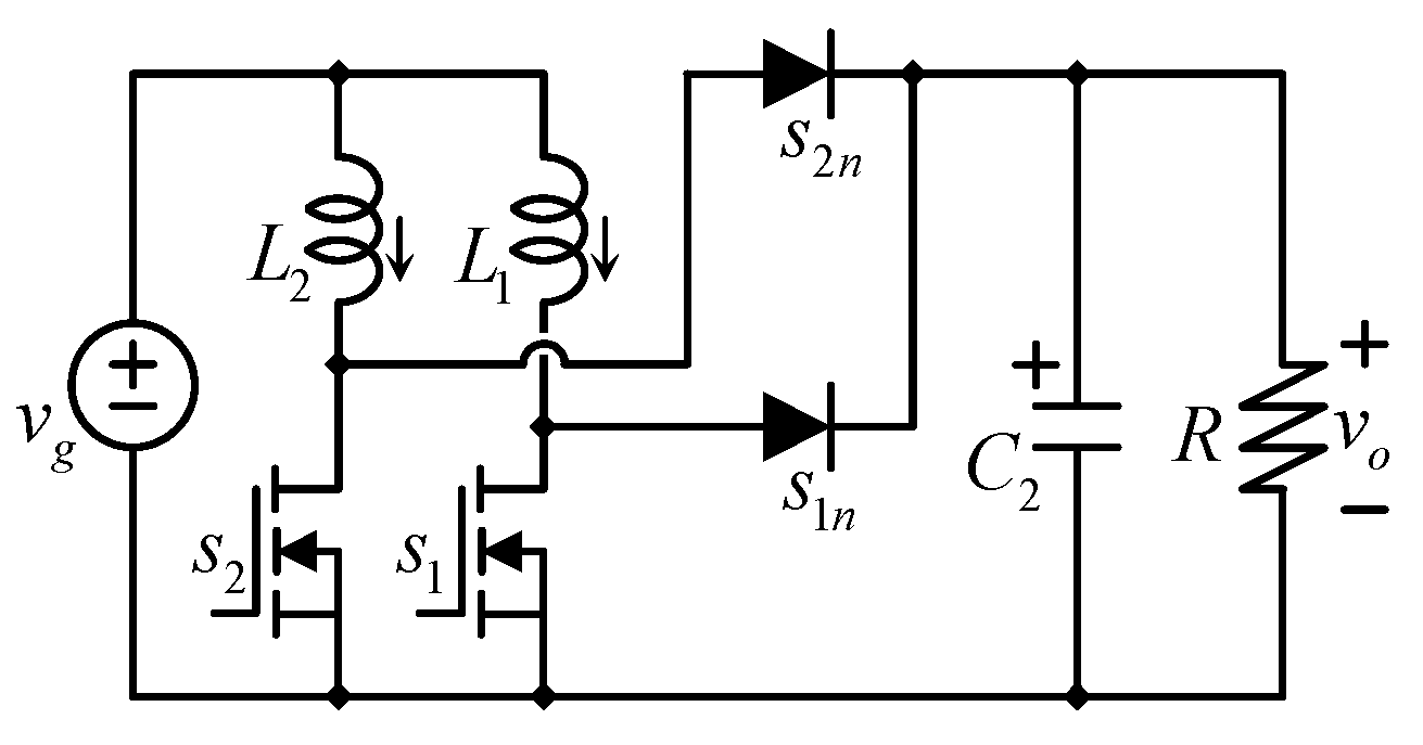
Figure 3 shows the topology. It is made by two inductors
L1 and
L2, which, in the traditional operation, have the same inductance, two capacitors
C1 and
C2 (capacitances are independent of each other in both the former and the proposed operation), two transistors
s1 and
s2, and two diodes
s1n and
s2n.
This topology has been recently proposed in both boost [
9] and its buck counterpart [
8]. In switched-mode power supplies, such as the converter understudy, diodes and transistors are fully open or closed at any time (unless they are changing the state from open to close or vice versa). Those components do not operate in the linear region of the semiconductor devices. In contrast, they operate like switches. The same applies to diodes, and they also act as switches. The switch complementary with transistors, which means when a transistor is closed, its complementary diode is open. When the transistor is open, their complementary diode is closed, the letter “
n” in the name of diodes indicates their complementary transistor,
s1n is complementary to
s1, and
s2n is complementary to
s2.
Switched-mode power supplies, such as the discussed converter, are controlled (driven) with digital switching-functions (functions of the time which) indicate when transistors open or close. Those switching functions are obtained by the comparison of DC signals with triangular waveforms.
The process in which switching functions are obtained is called pulse width modulation (PWM).
Figure 4a shows the block diagram of the pulse width modulation (PWM) method used in the traditional operation, and
Figure 4b shows important waveforms in this process.
The switching functions or PWM signals for transistors are obtained by comparing a DC signal called “
D” (which is a dimensionless signal that takes values between 0 to 1) against triangular carriers
TriCarr1 and
TriCarr2 (triangular waveforms that varies between 0 to 1), see
Figure 4a and the bottom of
Figure 4b. The switching function
s1 is equal to one or high (is a digital function that can only take values or 1 or 0), when
D is over
TriCarr1, the signal
s1 is zero when
D is below the signal
TriCarr1. The same principle applies to the switching function
s2.
From
Figure 3, by applying the Kirchhoff current law (KCL), it can be observed that the input current
ig, the current that flows from the input voltage source
vg, is equal to the sum of currents through inductors.
There is a 180° phase shift among triangular carriers, which allows canceling a portion of the input current ripple. For example, if switching functions were in phase (see the inductors currents in
Figure 4b), the input current would contain a large ripple (variation), since the input current would be the summation of ripples in individual inductors. The phase shift allows certain cancelation in the AC component of signals.
There are two switches which state determines the switching state of the entire converter, and then there are four possible combinations of the position of transistors, which are called switching states. The four possibilities are s1 = 1, while s2 = 0, which means transistor s1 is closed while s2 is open; the second possibility is to have s1 = 0 while s2 = 1; the third switching state is s1 = 1 and s2 = 1; and finally, when both signals are equal to zero (s1 = 0 and s2 = 0). During the operation, the number of switching states that appear depends on the duty cycles.
If the duty cycle is lower than 0.5, see
Figure 5a, in which the duty cycle is around 0.33, only three switching stages appear:
s1 = 1 and
s2 = 0,
s1 = 0 and
s2 = 1, and finally the state
s1 = 0 and
s2 = 0, which is marked in gray color in
Figure 5a.
If the duty cycle is equal to 0.5, see
Figure 5b, only two switching stages appear,
s1 = 1 and
s2 = 0, and
s1 = 0 and
s2 = 1; signals coincide in which transistors change their state at the same time.
If the duty cycle is larger than 0.5, see
Figure 5c, in which the duty cycle is around 0.66, only three switching states appear,
s1 = 1 and
s2 = 0,
s1 = 0 and
s2 = 1, and finally the state
s1 = 1 and
s2 = 1, which is marked in gray color in
Figure 5c.
Despite the four possible combinations of switch positions, reference [
9] recommends operating the converter only when
D ≥ 0.5. Reference [
17] explores the operation when
D < 0.5, and it founded that it is possible to operate it under this circumstance, but a reduction of the efficiency is observed. This article focuses on the operation when
D ≥ 0.5. In this case, the three equivalent circuits that appear during the operation are depicted in
Figure 6, along with a zoom in the PWM signals previously shown in
Figure 5c.
From the equivalent circuits shown in
Figure 6, and by following the KVL and KCL, the mathematical model of each equivalent circuit can be derived.
The mathematical model of the circuit shown in
Figure 6a is:
where
C1 and
C2 are, respectively, the capacitance of capacitors,
L1 and
L2 are, respectively, the inductance of inductors,
vC1 and
vC2 are, respectively, the voltage across capacitors
C1 and
C2;
iL1 and
iL2 are, respectively, the currents through inductors
L1 and
L2,
vg is the input voltage, and
io is the output current, the current through the output resistor which is equal to
vC2/R.
The inductance of inductors multiplied by the derivative of current through inductors is equal to the voltage across inductors terminals. In addition, the capacitance of capacitors multiplied by the derivative of voltages is equal to the current through capacitors.
The mathematical model of the circuit shown in
Figure 6b is:
The mathematical model of the circuit shown in
Figure 6c is:
Figure 6d shows a zoom intro PWM signals in
Figure 5c, which is the case under study. The duty cycle of the converter is larger than 0.5. This diagram is useful to determine the time period each equivalent circuit holds, with the final intention to provide an average mathematical model. The definition of the duty cycle
D is used in
Figure 6d, and the duty cycle can be defined as the relation of the time period in which a transistor is closed, divided over the total switching period. In the converter under study, both transistors have the same duty cycle. The remainder of the average time (in which the transistor is open) can be expressed as (1 −
D).
It can be observed that the time period in which the switching state
s1 = 0 and
s2 = 1 is equal to (1 −
D)
·TS (see the green labels); it can also be observed that the time in which the switching state
s1 = 1 and
s2 = 0 is equal to (1 −
D)
·TS (see the blue labels); finally, the time in which both transistors are on (
s1 = 1 and
s2 = 1), can be calculated as
DTS − (1 −
D)·
TS = (2
D − 1)
·TS (see the time marked with gray color besides and over the blue labels). In order to provide the average mathematical model, models for each switching state can be multiplied by the time each switching state holds and divided over the total switching period
TS. This leads to:
Note that the term
TS is not present since it is canceled during the averaging process. Furthermore, the lowercase “
d” is used instead of the uppercase “
D”. In general, lowercase letters are used to indicate that signals can change (are variables), and uppercase letters are used to indicate they operate in steady-state (are constant in this specific condition). The average model in (8)–(11) can be further simplified to the model in (12)–(15).
From the described dynamical model in (12)–(15) the steady state condition or equilibrium can be obtained, when derivatives are equal to zero, the equilibrium is determined as:
Notice that the equilibrium defines both inductor currents to be equal. On the other hand, in a traditional interleaved boost converter, an additional mechanism is usually required to prevent a severe current imbalance. This is one of the advantages of the discussed converter. The second advantage is that the blocking voltage of most transistors is half of the output voltage. This reduces the switching losses of transistors with the same switching frequency, and then the switching frequency can be increased without increasing the switching losses.
The Input Current Ripple
Like the interleaved boost converter, another advantage of the series-capacitor converter is its input current ripple cancelation feature. The ripple is a small variation due to the transistor’s switching action, which appears on the state variables (current through inductors and voltage across capacitors) and other variables (such as the input current and the output voltage). It is highly desirable to have a small switching ripple, since it has a negative effect on the electromagnetic compatibility of the entire grid-tied generation system (see
Figure 1). The ripple increases the RMS (root of the mean square) value of signals, which leads to additional energy losses in the case of the current (as the discussed case).
The input current ripple cancelation consists of a reduction of the input current ripple compared to individual inductors current ripple. See
Figure 4b: at the top of the figure, the input current is shown; the input current is equal to the summation of both currents through inductors, but the ripple is smaller in the input than in each inductor, thanks to the cancelation, in the case of the series-capacitor converter.
The ripple in each inductor can be calculated considering that their current rises when then their respective transistor is closed and hold rising for a time equal to
DTS; the derivative of the current or current slope in an inductor is equal to their voltage divided over their inductance
di/
dt =
V/
L. The current ripple through inductors
L1 and
L2 can be calculated as:
The number two in the denominator in (18) comes from the fact that the ripple is defined as the maximum deviation from the average current. The average is at the middle point in the triangular waveform. The peak-to-peak variation in
Figure 4 is indicated as twice of the ripple.
The input current ripple can be calculated at any switching state. Consider, instead, the state in which
s1 = 1 and
s2 = 0 (see
Figure 6b), this switching state holds for a time (1 −
D)
TS, and during this time, the current through inductor
L1 is rising with a slope equal to their voltage (
Vg at this moment) divided over their inductance
diL1/
dt =
Vg/
L1, while the current through
L2 is decreasing with a slope equal to (
Vg −
VC1)/
L2, the current is decreasing, since
VC1 is larger than
Vg. Then, the ripple can be calculated as (19).
Equation (19) can be simplified, considering inductors are equal (
L1 =
L2 =
L) to (20).
In addition, finally, the input current ripple can be normalized, with respect to the current ripple in inductors, by dividing (20) over (18) (and considering
L1 =
L2 =
L). The normalized input current ripple can be expressed as (21).
Figure 7 shows in black color the normalized input current ripple of the series capacitor boost converter (Equation (21)). The black line is shown only for duty cycles larger than 0.5, which is the focus of this article (as recommended in [
9]). The grey line color shown for duty cycles smaller than 0.5 corresponds to the classical interleaved boost converter, which has a similar normalized current ripple compared to the series capacitor boost for a duty cycle smaller than 0.5.
The maximum value of the normalized current ripple is equal to 1, indicating the current ripple’s input current ripple is equal to the current ripple in one inductor. In a traditional boost converter, the input current ripple is equal to the inductor current ripple, and then, having a smaller ripple is the advantage of interleaved topologies. Furthermore, when the current is split among different inductors, the maximum stored energy (which depends on the square of the current) decreases.
The current ripple reaches a zero point when
D = 0.5. At this point, the current ripple among inductors has a perfect cancelation. The PWM scheme’s important signals in this particular operation point are shown in
Figure 8, which is similar to
Figure 4.
3. The Series-Capacitor with Proportional Duty Cycles and Reduced Input Current Ripple
The current ripple cancelation is one of the main advantages of the series-capacitor boost converter, especially when it works in duty cycles near the D = 0.5 point; in some cases, the D = 0.5 point is not reached due to the voltage gain required for the converter.
A recent contribution to state of the art, related to the series capacitor converter, was a design technique that, along with a particular PWM strategy, allows moving the zero ripple point to a different value than D = 0.5. It can be, for example, 0.55, 0.6, etc.
This contribution was introduced in [
17], their main difference compared to the traditional operation is that in the proportional strategy, inductors may have different inductance. Being
L1 smaller than
L2 by a factor
k (the factor
k can take values between 0 and 1), and having different duty cycles for each transistor, the relationship of which is also
k. The converter still has a duty cycle
D, but the duty cycle
D1 of transistor
s1 and
D2 of transistor
s2 are different and defined as (22) (in which also the relation among inductors is defined).
Considering the described condition, and assuming that
D +
kD > 1 (this is equivalent to say that
D > 0.5 in the traditional operation), the dynamical model of the converter, which is expressed as (12)–(15) in the traditional operation, is now expressed as (23)–(26).
From the described model (23)–(26) the steady state condition or equilibrium can be obtained, when derivatives are equal to zero, the equilibrium is determined as (27)–(28).
The equilibrium makes inductors have different current but is still established in an equilibrium point, which prevents an overcurrent in an inductor. The current through each inductor can be calculated during the design process, and then each of them may be properly rated.
4. Differential Evolution Algorithm
Like most metaheuristic techniques, the differential evolution (DE) [
19,
20,
21,
22] is a population-based algorithm. The DE considers its members as vectors of parameters whose defined positions on a given multidimensional space are modified as the optimization process advances. The stages of the evolutionary process of the DE algorithm can be described through a series of steps: (1) the initialization of a population that stochastically and uniformly generates parameter vectors within the limits of the search space of the problem to be optimized; (2) the differential mutation on the elements of the population to achieve recombination between individuals; (3) the crossover of information between the elements of the population to increase population diversity; (4) an elitist selection mechanism where the best individuals will prevail in every generation.
Note: The terms crossover and recombination are used synonymously in the context of this article, which is a common practice in the evolutionary algorithms field [
20].
4.1. Initialization
Before the DE algorithm operators can be applied, it is necessary to initialize each of the population members. Thus, it is required to specify the limits of the search space for the optimization problem. These vectors represent the lower and upper limits for each dimension of the problem and are the constraints known as box constraints. The lower limits vector is represented by and the upper limits vector as .
Once the search space limits have been specified, a random number generation scheme is established to follow a uniform distribution among the generated results. This mechanism will assign a value to each position of the population members within the range specified by the lower and upper limits, as follows:
Here, and represent the lower and upper bound vectors, respectively. At the same time, denotes a vector of random numbers within the uniformly distributed interval [0, 1].
4.2. Mutation
Once the initialization process described in the previous section has been executed, the DE algorithm will use the mutation operator to recombine the elements of the population to produce a modified version of all the individuals. The mutation operator is also known as differential mutation since it is based on the difference between the parameter vectors. This mechanism promotes exchanging information between all the elements and guides the strategy search through the optimal global solution.
The generic model of differential mutation adds the scaled and randomly sampled difference between two vectors belonging to the population into a third vector from the same population. Thus, generating a fourth parameter vector known as a mutant vector, which results from a combination of the three vectors described above. The differential mutation takes the following mathematical description:
Here, , , and are different parameter vectors randomly selected from the population. On the other hand, F is the scale factor with values within the interval [0, 2], representing the so-called differential weight and controlling the magnitude of variation regarding the difference .
4.3. Crossover
The primary objective of the crossover operation is to increase the diversity of the parameter vectors. This fact indicates that the crossing operation complements the mutation strategy used, increasing the diversity of the population. For this operation, the mutant vector
and the individual
are subjected to a recombination process that considers an element-by-element exchange operation between both vectors to generate a test vector
. Such operation is calculated considering the following scheme:
Here, Pcross is the crossover parameter, which controls how much the mutant vector contributes to generates the test vector, and it takes values within the interval [0, 1].
The crossover operation randomly swaps positions between the individual and the mutant vector . In this process, the Pcross parameter indicates which positions of the mutant vector will be taken for the generation of the test vector , and which positions of the individual will be used for the same purpose.
4.4. Selection
The selection operation aims to keep the best solutions within the population throughout the optimization process. To perform this action, after the mutation and crossover operations have been executed, the test vector is a candidate to be part of the population if it meets an elitist selection criterion. In this criterion, it will be considered that the test vector will replace its previous version if it represents a better solution than its last version.
The selection criterion considers the calculated fitness value of the test vector
and the fitness value of the corresponding individual
. The decision is based on the following rule: If the fitness of the test vector is better than the fitness of the individual, then the test vector will replace the individual to become part of the population for the next generation. Otherwise, the vector
will remain in the population for at least one more generation. This selection mechanism is summarized in the following equation:
5. The Proposed Strategy for the Series-Capacitor with Independent Duty Cycles
This article introduces a change in the operation of the series-capacitor boost with proportional duty cycles, the change has no effect on the zero-ripple operation point, in which the input current ripple is still zero, but aims to reduce the input current ripple in other operation points. This is made by allowing duty cycles to be independent of each other. This section introduced the changes in the mathematical model required to apply the proposed method.
In a power converter, the relationship among duty cycles can be changed during the operation since the duty cycle is a signal calculated with the controller of the converter (for example, a computer or a microcontroller), but the relationship among inductors cannot be changed during the operation, since they are physical components.
The mathematical model introduced for the discussed operation requires a difference from [
17], two factors are introduced in this article: the relation among inductors
kL (which is a constant) and the relation among duty cycles
kd (which may vary); the equation described in this section are equivalent to [
17] if
kL =
kd =
k.
The converter still has a duty cycle
D, the relation among duty cycles
D1 and
D2, and among inductors is defined as (37).
Considering (37), and assuming that
D +
kD > 1 (this is equivalent to say that
D > 0.5 in the traditional operation), the dynamical model of the converter, which is expressed as (12)–(15) in the traditional operation and expressed as (23)–(26) in the proportional-duty cycle operation, is now expressed as (38)–(41).
In addition, from the described model (38)–(41) the steady state condition or equilibrium can be obtained; when derivatives are equal to zero, the equilibrium is determined as (42)–(43).
5.1. The Input Current Ripple in the Proposed Strategy
The ripple in each inductor still can be calculated considering that their current rises when then their respective transistor is closed, but now, the equation must consider each transistor hold closed at a different time, and in this case, they are expressed as (44).
Notice that (44) contains both definitions, in terms of D1, L1, D2, and L2, and the definition in terms of D, kd, L, and kL.
Signals are similar to previous cases, but the input current ripple has to be defined in two different cases, the case when s1 = 1 and s2 = 0, and the case when s1 = 0 and s2 = 1; those two cases must be considered, and the larger variation must be considered as the ripple.
Let us consider first the time in which
s1 = 1 and
s2 = 0 (see
Figure 6b), this switching state holds for a time (1 −
D)
TS (see
Figure 9b), and during this time, the current through inductor
L1 is rising with a slope equal to
Vg divided over
L1, while the current through
L2 is decreasing with a slope equal to (
Vg −
VC1) divided over
L2, this leads to (45).
Notice that (45) already considers L2 = L and L1 = kLL.
During the second case, in which
s1 = 0 and
s2 = 1 (see
Figure 6a), this switching state holds for a time (1 −
kdD)
TS (see
Figure 9b), and during this time, the current through inductor
L2 is rising with a slope equal to
Vg divided over
L2, while the current through
L1 is decreasing with a slope equal to (
Vg +
VC1 −
VC2) divided over
L1; this leads to (46).
Finally, in this case, there is not a normalized current ripple; since the current ripple in inductors is now different, it would be equal if kd = kL, but since kd is a variable because duty cycles are independent, then this equivalency cannot be established.
5.2. The Objective Function
Once it has been established that duty cycles will be independent (or, in other words, that kd is a variable), then kd may be used to minimize the input current ripple. However, question arises; now, there is an infinite number of combinations of duty cycles to achieve the same voltage gain. The differential evolution algorithm can be used to determine the solution. The expected solution is the D and kd (alternatively, the D1 and D2).
The provided solution must comply with the desired output voltage; for a given input voltage, this can be expressed as a voltage gain; the output voltage of the converter is the voltage in capacitor
C2 expressed in (42) and repeated here for convenience.
In addition, at the same time, to minimize the input current ripple, which is the largest value of any of the ripple expressions in (45) and (46), considering the equilibrium described in (42) and (43), the ripple expressions can be rewritten as (48) and (49).
Under the above assumptions, the objective function can be formulated as the minimum input current ripple provided by some
D and
kd parameter values. This expression is shown in (50).
To satisfy the desired output voltage, the constraint given by (51) contemplates an acceptable tolerance that considers 1% of the expected voltage gain.
5.3. The Proposed Optimization Strategy
The optimization problem is formulated as the search for the optimal duty cycle values that reduce the input current ripple of the series-capacitor boost. This reduction is possible if the input current ripple is reformulated, considering duty cycles D1 and D2 (alternatively D and kd) independent. This change does not affect the zero-ripple operation point, but it aims to reduce the input current ripple in other operation points while achieving the desired voltage gain. However, having independent duty cycles leads to a problem with infinite possible solutions. Therefore, to find the optimal combination of parameters D and kd, the DE algorithm is proposed. In the optimization process, every individual from the population is made up of a combination of these two parameters, so that
Different from other evolutionary algorithms, the DE method is much simpler and straightforward to implement. Simplicity and low computational cost are essential in real applications, since this allows real-time implementations by non-experts in evolutionary computation or non-experts programmers. Besides, the DE algorithm is not only simple, but also popular for its successful performance in finding feasible solutions to complex and real optimization problems.
The proposed method can be implemented offline to find the optimal duty cycles for a predefined operation range. After that, these values can be used in real-time to reduce the input current ripple of the converter. It is also possible to implement the optimization in real-time if the converter has enough computational resources to support the complete process.
In the optimization process, every individual from the population is made up of a combination of these two parameters so that
A population of size
N is randomly initialized within the lower and upper limits. Then, each individual is evaluated in the objective function to determine its quality as a candidate solution. However, the optimization problem is constrained. Therefore, if a candidate solution does not satisfy the requirements, it must be penalized in order to guide the search through feasible solutions. Thus, the proposed optimization strategy implements a penalty function that increases the fitness value of every candidate solution that does not accomplish the constraints. Under such considerations, the objective function is reformulated as follows:
Here,
h is the penalty function that modifies the fitness value of the individuals that cannot be considered possible solutions. The definition of the penalty function is expressed as follows:
From the penalty function,
W is a weighted factor that regulates how much the candidate solution is penalized. On the other hand,
C is the activation function that determines if an individual has violated or not the constraint from (51). The activation function is defined as:
Under the DE scheme, individuals from the population are updated by applying the mutation and crossover operators. The solutions with the best fitness values are selected to be part of the next generation. The process is repeated until the maximum number of generations
Gmax is reached. At the end of the optimization process, the best duty cycle combination resides in the best-found solution. A summary of the entire process is described in Algorithm 1.
| Algorithm 1. Optimization strategy using DE. |
| Initialize parameters , W, N, Gmax |
|
Initialize population
|
|
Evaluate the population in the objective function
|
|
For each individual from the population
|
|
----Generate a mutant vector |
|
----Generate a trial solution |
|
----Select the best solution between and |
|
End for
|
|
Update the global-best so far
|
|
If the maximum number of generations has not been reached
|
|
----Go to step 4
|
|
Else
|
|
----End the optimization process
|
|
End if-else
|
|
Output: the global-best solution so far |
6. Results
Several numerical tests were made to validate the performance of the proposed method. The objective is to demonstrate that the same converter (without changing any physical parameter), with the proposed operation (which would represent an operative instruction “software” change), achieves the desired voltage gain and a smaller input current ripple. The example considers the case in which a variable-voltage energy-source feeds the converter within a range of 30 V to 40 V. This voltage may come from commercial Fuel Cell FC stacks; for example, see [
23] (p. 25) and [
24] (p. 25), which are specific FC stacks of the family described in [
3]. The converter must feed an H-bridge inverter with a voltage of 200 V to produce a 120 V AC voltage. This would require the converter to operate in a variable voltage gain within a range of 5 to 6.6667.
In the proposed work, the DE algorithm is implemented to reduce the input current ripple while achieving the desired voltage gain. The DE algorithm is a method well-known by the evolutionary community that has proven its effectiveness in multiple applications [
25]. It is characterized for its simplicity, and its robustness has been supported by many research works over the years [
26].
The implementation of the DE algorithm requires some initial values for the input parameters. These parameters are the crossover probability Pcross, the constant factor W, the size of the population N, and the maximum number of generations Gmax. The parameter configuration has been established considering the performance of the DE algorithm, which is measured according to the obtained input current ripple value Δig in every operating point. Since the objective is to reduce the input current ripple as much as possible, we have chosen the parameter value combination that best contributes to reaching the lowest possible input current ripple. A sensitivity analysis was performed to select the most appropriate parameter values in which different value combinations were tested, considering each operating point. Thus, the best parameter combination was found under a sensitivity analysis in which different values within a specific range were tested to observe the DE algorithm’s performance.
In the first stage, the analysis was made using only the crossover probability
Pcross, and the constant factor
W. Since the crossover probability recommended by the author of the DE algorithm is 0.2, a lower (0.1) and higher (0.3) value than the one suggested were used in the analysis. Regarding the constant factor parameter, the values 10, 100, and 1000 were used in order to include different penalty levels in the objective function. The test was carried out considering all possible combinations of these parameters in all operating ranges. Furthermore, due to the stochasticity of the proposed method, the test was executed 50 times using each parameter setting for each operating point. A sample of the results obtained from this analysis is shown in
Table 1,
Table 2 and
Table 3. These results report the average of the 50 independent executions and correspond to the sensitivity analysis at operating points
G = 5,
G = 5.5
, and
G = 6.
From
Table 1,
Table 2 and
Table 3, it can be seen that a lower crossover probability promotes less diversity in the population, causing the DE algorithm to stagnate in suboptimal solutions, generating higher input current ripples. On the other hand, as the crossover probability increases, the diversity grows, which can cause the DE algorithm to overexploit the search space and fail to refine the solutions, which also generates high input current ripples. For this reason, a probability with an intermediate value produces better results when analyzing the performance of the DE algorithm.
From
Table 1,
Table 2 and
Table 3, it is also observed that a low constant factor penalizes unfeasible solutions insufficiently. This can cause the DE algorithm to take longer to find better solutions since a lower penalty can guide the search more slowly towards the space of the feasible solutions. In contrast, a higher penalty can destabilize the algorithm, making it difficult to successfully search for feasible solutions. Therefore, this value must be balanced to obtain the best performance of the DE method.
This analysis shows that the best parameter combination occurs when the input current ripple reaches its lowest value, consistent when the crossover probability is configured with a value of 0.2 and the constant factor with 100. Similar results were obtained in the analysis considering the entire operating range. Therefore, a value of 0.2 has been assigned to the crossover probability since the method achieves its best performance under this configuration. Regarding the constant factor W, its set value is 100 since the best results were obtained when W equals 100.
In the second stage of the analysis, once the values of the two previous parameters had been chosen, the analysis was made for different numbers of generations and population sizes, where a population variation ranges from 20 to 50. In contrast, the number of generations varies from 100 to 500. Furthermore, due to the stochasticity of the proposed method, the test was executed 50 times using each parameter setting. The average of the 50 independent executions has been reported in
Table 4 and
Table 5. This analysis was carried out for the entire operating range. However,
Table 4 and
Table 5 only report the results obtained for the operating point
G = 5.
As expected, from
Table 4, it is evident that the larger the population size, the better the results obtained. However, using a bigger population represents a higher computational cost. In addition, since the optimization problem is not high dimensional, using a large population is not justified. Besides, the difference between the obtained results from different population sizes can be considered not significant enough to choose a larger population. For this reason, we have selected a population of 20, intending to reduce the computational cost and leave open the possibility of executing the proposed method in real-time for an application.
From
Table 5, it is clear that as the number of generations increases, the results improve. This situation is as expected because the solutions are refined over time by the search strategy of the DE algorithm. However, the solutions do not improve any further at a certain point, which indicates that no more generations are required because the algorithm has found an optimal solution. From the results obtained, it can be observed that after 300 generations, the improvement of the results is no longer significant. Thus, no more generations are required. This behavior can be observed in
Figure 11, which shows a convergence graph of the DE algorithm considering the analysis for the operating point
G = 5 on a single execution. The figure illustrates how, after 300 generations, the value of the best solution found stabilizes and no longer improves. Similar results were obtained for the rest of the operating points. Therefore, the number of generations was set to 300.
To summarize, the parameter values in which the DE algorithm’s best performance was achieved were used in the numerical experiments proposed in this article. These values are reported in
Table 6.
Additionally, the design of the voltage-doubler boost converter requires setting up some parameters such as the input voltage, the inductor constant factor, the switching frequency, and the inductance. The values of such parameters have been set according to the standard data usually used for real applications, see
Table 7.
In the experiments, the former and the proposed strategy have been tested using the parameter settings described above. Additionally, the popular particle swarm optimization (PSO) algorithm [
27] has been included in the experiments to compare the performance of the proposed method with another similar metaheuristic algorithm. All techniques have been evaluated considering the same conditions in order to ensure a fair comparison. The former approach has been executed once for each operating point. In contrast, the proposed method and the PSO have been run 30 times due to their stochasticity. The obtained results considering the best outcomes of the proposed technique, the former strategy, and the PSO method are reported in
Table 8. The best input current ripple Δ
ig reached among the three methods has been highlighted in boldface.
Table 8 shows that the proposed method achieves a lower input current ripple value than the former strategy in all operating points without changing the physical parameter of the converter. These results are because the DE algorithm manages to find an appropriate value combination of parameters
D and
kd. These values tend to minimize the input current ripple while achieving the desired voltage gain.
Furthermore, the proposed method achieves better results than the PSO algorithm in 26 of 35 operating points, proving its superiority and robustness. These results are because the DE algorithm handles a better search strategy than the PSO. In general, algorithms like DE or PSO work very well on unconstrained problems. However, some evolutionary algorithms do not work effectively when dealing with constrained applications, causing them to get stuck into infeasible or suboptimal solutions during the search process. Nevertheless, the DE algorithm has gained popularity because it produces feasible and optimal results even in constrained optimization problems.
Simulation of Some Operation Points
A converter was simulated in the software Synopsys Saber in order to observe and measure the new waveforms. The results demonstrate that the optimization reduces the input current ripple without making changes to the converter parameters.
Figure 12 shows the software implementation of the converter. Diodes have what in the power electronics field is called synchronous rectification, and switches are synthesized with the power semiconductor (name of the element in Synopsys Saber).
The output voltage is adjusted to 200 V, and a 200 Ω resistor is used as a load. The PWM scheme is shown in
Figure 13, it has an input for the duty cycle D, and for the relation among duty cycles
kd; this is the way the PWM can be implemented in practice.
Case
G = 5, in the former strategy: for the operation point in which the input voltage is 40 V, the output is 200 V, and the relation among inductors
kL = 0.5, the gain
G = 5 (see
Table 8), the former strategy would need a duty cycle
D = 0.7101 (
kd = 0.5), which would result in an input current ripple Δ
ig = 0.5212.
Figure 14 shows a zoom in the input current ripple for the former strategy. The point-to-point measurement indicates the peak-to-peak current ripple. The peak-to-peak ripple is twice of Δ
ig.
Table 8 indicates 0.5212, multiplied by two, would be 1.0424; the measurement indicates 1.0422.
The simulator contains elements with non-ideal parameters, and it is normal to have a slightly smaller value. The smaller value does not affect the operation since the ripple is calculated for a maximum value. It is acceptable if the real value is smaller than the theoretical value. We can conclude that the simulation demonstrates the values in
Table 8.
Case
G = 5, in the new strategy: for the same parameters of
Figure 14,
Figure 15 shows a zoom in the input current ripple for the proposed strategy, in this case,
D = 0.7070 (
kd = 0.5240) (see
Table 8); the input current ripple is Δ
ig = 0.4846 according to
Table 8. The point-to-point measurement in
Figure 15 indicates the peak-to-peak current ripple, which is twice of Δ
ig, 0.4846, multiplied by two, would be 0.9692; the measurement indicates 0.9678.
Case
G = 5.9, in the former strategy: for the operation point in which the input voltage is 33.90 V, the output is 200 V,
kL = 0.5, (see
Table 8), the former strategy would need a duty cycle
D = 0.7663 (
kd = 0.5), which would result in an input current ripple Δ
ig = 1.0132.
Figure 16 shows a zoom in the input current ripple for the former strategy. The point-to-point measurement indicates the peak-to-peak current ripple, which is twice of Δ
ig;
Table 8 indicates 1.0132, multiplied by two, would be 2.0264; the measurement indicates 2.0261.
Case
G = 5.9 in the new strategy: for the same parameters of
Figure 16,
Figure 17 shows a zoom in the input current ripple for the proposed strategy, in this case,
D = 0.7602 (
kd = 0.5612) (see
Table 8); the input current ripple is Δ
ig = 0.9508, according to
Table 8. The point-to-point measurement in
Figure 15 indicates the peak-to-peak current ripple, which is twice of Δ
ig, 0.9508, multiplied by two, would be 1.9016; the measurement indicates 1.9021.
Case
G = 6.5, in the former strategy: for the operation point in which the input voltage is 30.08 V, the output is 200 V,
kL = 0.5 (see
Table 8); the former strategy would need a duty cycle
D = 0.7994 (
kd = 0.5), which would result in an input current ripple Δ
ig = 1.1976.
Figure 18 shows a zoom in the input current ripple for the former strategy. The point-to-point measurement indicates the peak-to-peak current ripple, which is twice of Δ
ig.
Table 8 indicates 1.1976, multiplied by two, would be 2.3952; the measurement indicates 2.3949.
Case
G = 6.5, in the new strategy: for the same parameters of
Figure 16,
Figure 19 shows a zoom in the input current ripple for the proposed strategy, in this case,
D = 0.7921 (
kd = 0.5778) (see
Table 8); the input current ripple is Δ
ig = 1.1320 according to
Table 8. The point-to-point measurement in
Figure 15 indicates the peak-to-peak current ripple, which is twice of Δ
ig; 1.1320, multiplied by two, would be 2.2640; the measurement indicates 2.2631.


 ,
, 


