Article

Polypyrrole Film Deposited-TiO2 Nanorod Arrays for High Performance Ultraviolet Photodetectors

1
Guangzhou Key Laboratory of Sensing Materials & Devices, Center for Interdisciplinary Health Management Studies, School of Chemistry and Chemical Engineering, Guangzhou University, Guangzhou 510006, China
2
School of Chemical Engineering and Light Industry, Guangdong University of Technology, Guangzhou 510006, China
3
Guangzhou Institute of Software Application Technology, No. 1121 Haibin Road, Nansha District, Guangzhou 511400, China
4
Key Laboratory of Pulp and Paper Science & Technology of Ministry of Education, State Key Laboratory of Biobased Material and Green Papermaking, Qilu University of Technology (Shandong Academy of Sciences), Jinan 250353, China
*
Authors to whom correspondence should be addressed.
Chemosensors 2022, 10(7), 277; https://doi.org/10.3390/chemosensors10070277
Submission received: 6 June 2022 / Revised: 5 July 2022 / Accepted: 11 July 2022 / Published: 13 July 2022

Abstract

:
TiO2-based ultraviolet photodetectors have drawn great attention and are intensively explored. However, the construction of TiO2-based nanocomposites with excellent ultraviolet responses remains challenging. Herein, a TiO2 nanorod array was successfully prepared on fluorine-doped tin oxide (FTO) conductive glass by a one-step hydrothermal method. Then, polypyrrole (PPy)-TiO2 nanorod array composites were designed via subsequent in situ oxidative polymerization. The morphologies, structures, and photocurrent responses of the nanocomposites were systematically investigated. The results demonstrated that polypyrrole-TiO2 exhibited a stronger photocurrent response than pure TiO2 due to the p-n junction formed between n-type TiO2 nanorod arrays and p-type polypyrrole. The PPy-TiO2 composite obtained by deposition three times had the best photoelectric properties, exhibiting good performance with a sensitivity of 41.7 and responsivity of 3.5 × 10⁻³ A/W. Finally, the mechanism of the photoelectrical response of PPy-TiO2 composites was discussed, guiding the design of high-performance TiO2-based ultraviolet photodetectors.

1. Introduction

The basic working principle of ultraviolet (UV) photodetectors is that light is irradiated on photoresponsive material, which absorbs the energy of the photon and can excite photogenic electron-hole pairs thus showing the current signal, which can be applied to the detection of the light signal. UV photodetectors have gained intensive interest in the fields of industrial manufacture, biological detection, and environment monitoring due to the coupling merits of high sensitivity, good selectivity, and low cost [1,2,3]. The performance of UV photodetectors is closely related to the structure and properties of photosensitive materials. In recent years, diverse wide bandgap semiconductors such as SiC, GaN, ZnO, NiO, and TiO2 have been widely applied in the fabrication of UV photodetectors [4,5,6,7,8]. Among them, TiO2 has received widespread attention because of its tunable nanostructure, non-toxicity, and chemical stability [9,10,11]. However, the low mobility and high recombination rate of photogenerated carriers in TiO2 greatly hinder its application performance in UV photodetectors.
The photoresponse performance, sensitivity, and stability of UV photodetectors can be significantly improved by constructing a semiconductor heterojunction. Bulk TiO2 is a typical n-type semiconductor material. The p-n heterojunction can be constructed using an in situ composite with a p-type conductive polymer to improve its photoelectric response. The Schottky heterojunction can be constructed using a recombination of metal nanoparticles to provide it with excellent photoelectric response performance. So far, tremendous efforts have been made to design high-performance TiO2-based UV photodetectors by constructing p-n junctions, Schottky junctions, and heterojunctions for their fast photo-excited electron-hole pair separation [12,13,14,15,16]. Yang et al. [15] fabricated all-solid-state NiO/TiO2 heterojunctions with the NiO layer above or below TiO2 nanoarrays, and the fabricated devices demonstrated high detection sensitivity, fast photoresponse time, and self-powered performance. Wang et al. [16] assembled a UV sensor based on vertically aligned TiO2 nanowire arrays interconnected with ZnO nanosheets, which achieved UV light sensing performance. In addition to metal oxides, conducting polymers with good conductivity and reversible chemical states have also been used to improve the UV response of TiO2 [17,18,19,20,21]. Che et al. [20] fabricated TiO2 nanoarrays/PEDOT-type conducting polymers composites via electrochemical polymerization, which achieved good UV photo-detection performances. Kareem et al. [21] synthesized a nanocomposite composed of polypyrrole (PPy) nanofibers and TiO2 nanoparticles, which showed improved optical sensitivity. These results indicate that UV photodetectors with good performance can be obtained by constructing semiconductor composite materials, especially by constructing heterojunctions.
The formation of a heterojunction is closely related to the interface contact state of semiconductor composites. Therefore, high efficiency, large scale, and stable construction of nano-composites with controllable microstructure and morphology are the premise of preparing photoelectric devices with excellent performance by developing an appropriate preparation process. Good interface contact is the prerequisite for the formation of a stable heterojunction. The spin-coating method is simple and easy to operate, which can fabricate composite devices on a large scale, but the interface contact is difficult to control. Electrochemical in situ polymerization has the advantages of high efficiency, simplicity, and easy operation, but it has a narrow application range and can be applied to fewer systems. The interface contact formed by in situ chemical polymerization is close and stable, but the efficiency of this method is low. In our previous research, TiO2/PANI nanocomposites with controllable microstructure were successfully prepared by in situ chemical polymerization and low-speed spin coating, which showed excellent photoelectric response performance. These works provide a solid foundation for further preparation of other TiO2 composites and the study of their photoelectric response properties.
The above findings demonstrated that the interface contact between the conducting polymer and TiO2 would greatly influence the optical properties of their nanocomposites. Therefore, it is highly desired to develop suitable approaches to tailor interface bonding of PPy-TiO2-based nanocomposites for high-performance UV photodetectors. In this work, we first successfully prepared TiO2 nanoarrays with regular microstructure through a simple hydrothermal method. Additionally, then PPy film-coated-TiO2 nanorod arrays were successfully synthesized via in situ oxidative polymerization. The thickness of PPy film can be effectively controlled by the number of deposition times. The structural characteristics and the optical properties of the as-prepared PPy-TiO2 nanocomposites were systematically investigated.

2. Materials and Methods

2.1. Chemical Reagents

Acetone (AR, 99.8%), anhydrous ethanol (AR, 99.5%), and hydrochloric acid (37 wt.%) were purchased from Guangzhou Chemical Reagent Factory (Guangdong, China). Titanium butoxide (AR, 98%) was purchased from Shanghai Macklin Biochemical Co., Ltd. (Shanghai, China), and pyrrole (Py, AR, 98%) and ammonium persulfate (APS, AR, 99%) were purchased from Shanghai Aladdin Biochemical Technology Co., Ltd. (Shanghai, China). All reagents were used directly without further treatment. Fluorine-doped tin oxide (FTO) substrates were purchased from Nippon Sheet Glass Co., Ltd. (Osaka, Japan).

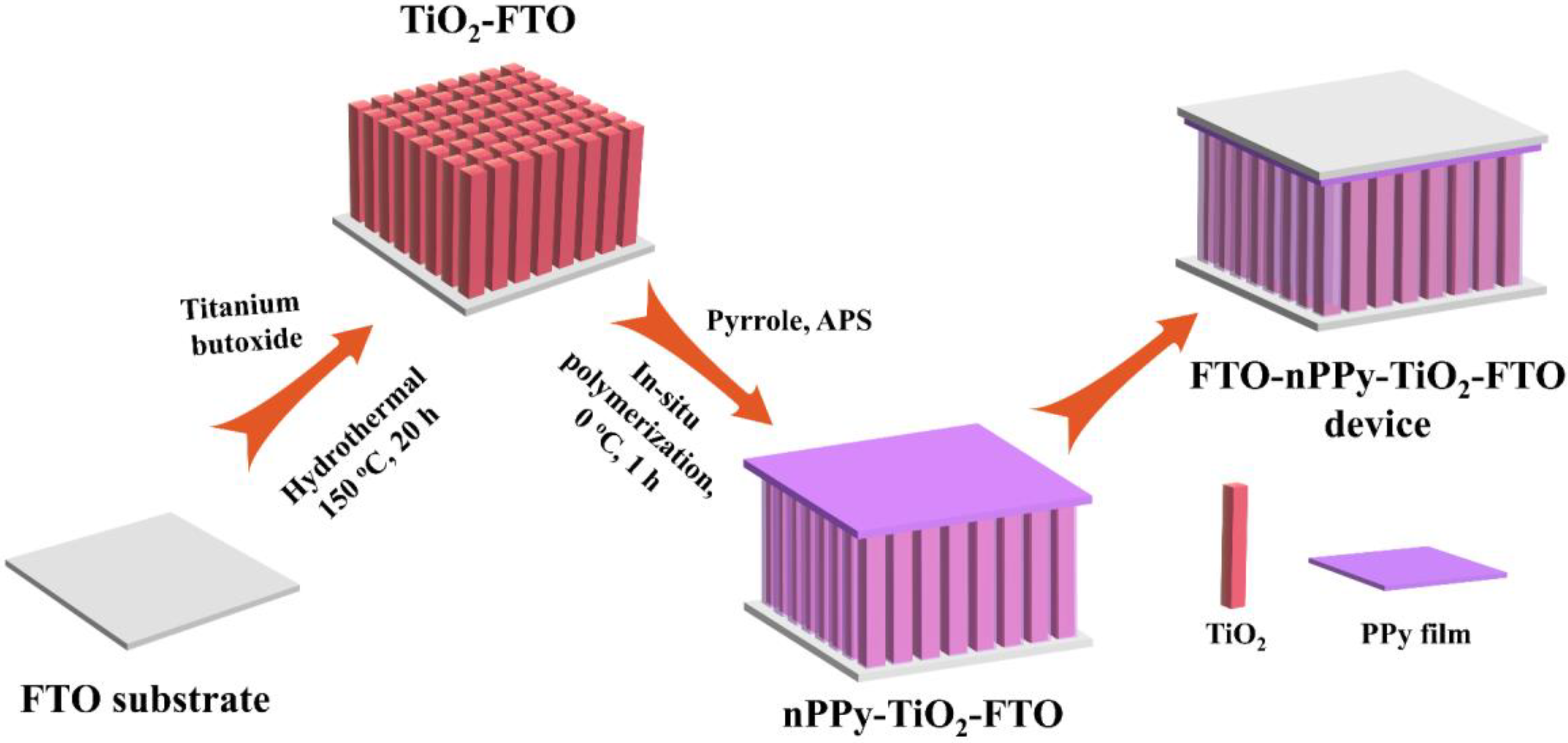
2.2. Preparation of the TiO2 Nanorod Arrays

TiO2 nanorod arrays were synthesized via a simple hydrothermal method [22]. Fluorine-doped tin oxide (FTO) substrate (25 mm × 25 mm, Nippon Sheet Glass Co., Ltd.) was ultrasonically cleaned for 30 min in acetone, ethanol, and deionized water thrice and was placed into a Teflon-liner stainless steel autoclave. A mixed solution of 30 mL of deionized water, 30 mL of HCl (~37 wt%), and 1 mL of titanium butoxide was then poured into the autoclave. The autoclave was sealed and transferred to an oven at 150 °C for 20 h. After the autoclave cooled down to room temperature, the FTO substrate was taken out and rinsed with deionized water five times to obtain TiO2 nanorod arrays grown on the FTO substrate.

2.3. Preparation of the PPy-TiO2 Nanocomposites

PPy-TiO2 nanocomposites were synthesized via in situ oxidative polymerization as follows: Firstly, 160 μL pyrrole were added to 20 mL of 1 M HCl and stirred for 1 min. Secondly, the prepared TiO2 nanorod arrays were placed in the above solution, and 1.5 mL of 0.1 M APS solution were dropped into the solution. Subsequently, the mixed solution was placed into a refrigerator at 0 °C for 1 h to acquire PPy-TiO2 nanocomposites. By controlling the reaction times, nPPy-TiO2 nanocomposites obtained by different deposition times were prepared, where n represented the deposition times (n = 1, 2, 3, and 4).

2.4. Fabrication of the FTO-nPPy-TiO2-FTO Device

The schematic diagram of the fabrication of the FTO-nPPy-TiO2-FTO device is shown in Figure 1. A cleaned FTO substrate was taken, and its conductive surface was fixed face to face with the nPPy-TiO2 nanocomposites on FTO to obtain the FTO-nPPy-TiO2-FTO photodetectors. For comparison, the FTO-TiO2-FTO device was fabricated using a cleaned FTO substrate and the FTO substrate that coated the TiO2 nanorod arrays.

2.5. Characterization

The morphologies of the samples were observed by scanning electron microscopy (SEM, JEOL, JSM-7001F, Rigaku Tokyo, Japan) and transmission electron microscopy with energy-dispersive spectroscopy (TEM, FEI Talos F200X, Thermo Fisher Scientific, USA). For the TEM measurement, the PPy-TiO2 composite was first scraped off the FTO substrate, then dispersed in anhydrous ethanol, and the supernatant was dropped onto a copper mesh after 1 h of sonication and air-dried for use. The structural characteristics of the samples were examined by Raman spectroscopy (LabRAM HR800, HORIBA Jobin Yvon, Japan). The crystalline structures of the samples were characterized by X-ray diffraction (XRD, Bruker D8 Advance, Germany). The surface properties of the samples were studied by X-ray photoelectron spectroscopy (XPS, Thermo Scientific K-Alpha, Thermo Fisher Scientific, USA), where the charge correction was based on a binding energy of 284.8 eV for C1s. UV-Vis absorption spectra of the samples were recorded using a UV-Vis spectrophotometer (UV 2450, Shimadzu, Japan). Photoluminescence (PL) spectra were used to investigate the optical properties of the samples (FluoroMax-4, HORIBA Jobin Yvon, Japan). The photoelectric performances of the fabricated devices were measured by a CHI660D electrochemical workstation (Chenhua, Shanghai), where electrochemical impedance spectroscopy (EIS) was performed at the open-circuit voltage of the device; the test frequency ranged from 0.01 to 100,000 Hz, and the amplitude was set to 5 mV. The UV light source was provided by a portable UV lamp (~8W, ENF-280C, Spectronics, USA). The overall sensing area of the fabricated UV photodetector was about 1.5 cm2. The UV light irradiated the device at an incident angle of 30°.

3. Results and Discussion

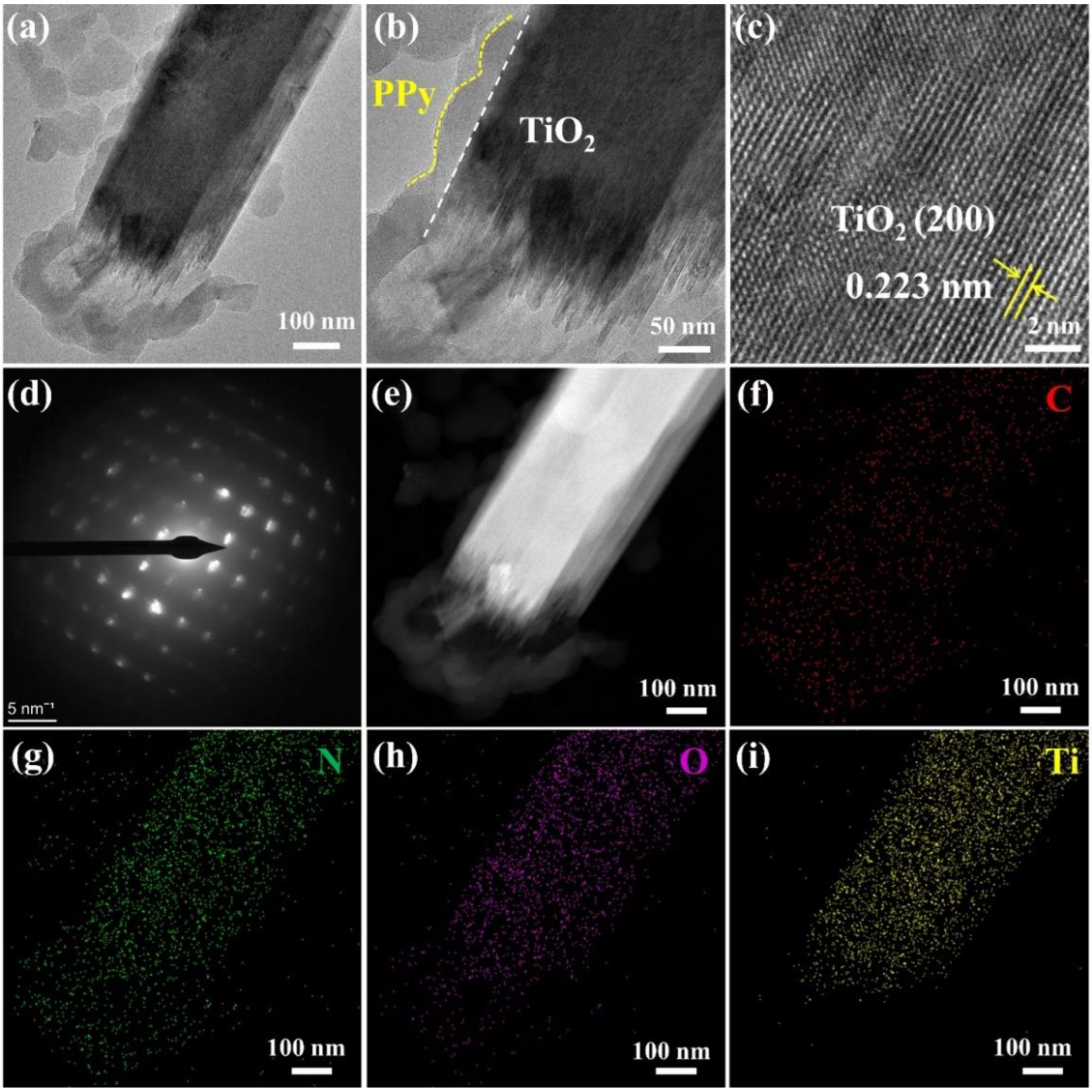
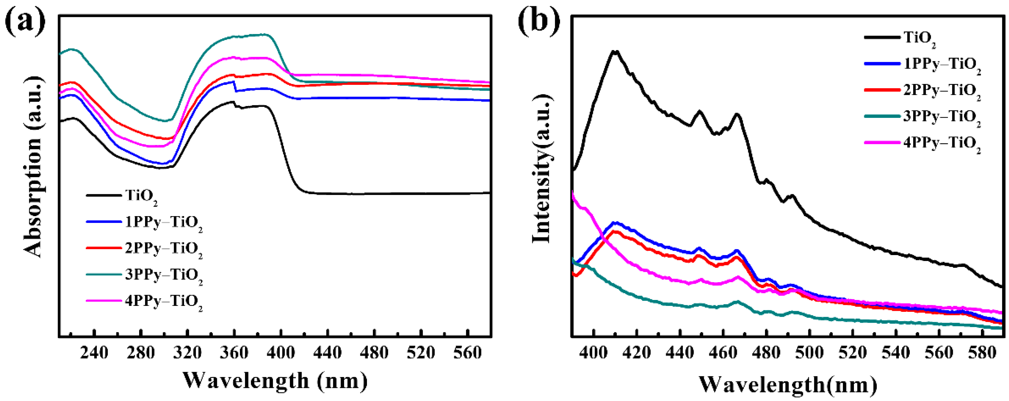
3.1. Structural and Optical Properties of the PPy-TiO2 Nanocomposites

The cross-sectional morphologies of all the nPPy-TiO2 nanocomposites prepared by different deposition times were first observed by SEM, as shown in Figure 2. Both samples showed similar morphologies, where PPy film was deposited on the surface of TiO2 nanorods, and the thickness of the PPy layer can be effectively controlled from 20 nm~200 nm. With the increasing deposition times, the thickness of PPy film that coated the surface of TiO2 nanorod arrays gradually increased, and the TiO2 nanorod arrays remained neatly arranged. It can be seen that uniform PPy film was deposited on the TiO2 nanorods in 3PPy-TiO2 owing to the strong hydrogen bonding interaction between the hydroxyl groups on the TiO2 surface and PPy, but with further deposition, aggregated PPy particles appeared in 4PPy-TiO2 due to the completely covered binding sites on the TiO2 surface, which indicated that the optimized deposition times were three times. The above results suggested that the morphologies of the PPy-TiO2 composites can be precisely regulated by the number of PPy depositions. TEM measurement was further conducted to study the interfacial recombination between the PPy and TiO2. The TEM images in Figure 3a,b further revealed the microstructure of 3PPy-TiO2, where a well-defined composite interface labelled by yellow and white lines between the PPy and TiO2 array could be observed, indicating the good compatibility of the composite. The TiO2 array was composed of a large number of small nanorods with sizes of about 5 nm and lengths of about 1.1 μm (Figure S1), which is conducive to receiving more light stimulation and thus enhancing the photo response performance. The clear lattice fringes of the HRTEM image in Figure 3c demonstrated that the deposition of PPy would not destroy the lattice structure of titanium dioxide. The interlayer spacing of 0.223 nm in Figure 3c was assigned to the (200) crystal plane of rutile TiO2, and the corresponding selected area electron diffraction pattern in Figure 3d show its typical single-crystal characteristics. Furthermore, the STEM image in Figure 3e and the elemental mapping images in Figure 3f–i show the uniform distribution of C, N, O, and Ti elements, suggesting uniform PPy deposition on TiO2 nanorods. This might favor the good optical property of 3PPy-TiO2.
Raman spectroscopy was conducted to examine the structural properties of pure TiO2 and nPPy-TiO2 nanocomposites. As illustrated in Figure 4a, pure TiO2 showed three peaks at 228, 435, and 598 cm−1 assigned to the characteristic signals of rutile TiO2 [23,24]. After PPy deposition, these three peaks were slightly blue-shifted, indicating the existence of chemical bonding between PPy and TiO2 nanorods. The chemical bonding may result from the hydrogen bonding between the amino group of PPy and the surface hydroxyl group of TiO2, and the light scattering ability of TiO2 was changed. Several new peaks attributed to PPy also appeared in the range of 800~1800 cm−1. Namely, characteristic peaks at 930, 1050, 1080, and 1252 cm−1 were the result of C-H deformation vibration in PPy [25,26], the double peak at 1374 and 1332 cm−1 was the ring stretching vibration peak of pyrrole [27,28], and the single peak at 1595 cm−1 was indexed to the C=C stretching vibration of pyrrole ring [29,30]. Furthermore, the characteristic peak intensity of TiO2 in the nPPy-TiO2 composites gradually weakened with the increased deposition times, indicating that rutile TiO2 had been completely covered by the newly generated PPy film. All XRD patterns in Figure 4b show diffraction peaks at 2θ = 37.7°, 39.4°, 56.1°, 64.4°, 70.6°, and 71.4° that can be indexed to (101), (200), (220), (310), (301), and (112) crystal planes of rutile TiO2 (JCPDS No. 21-1276) [8], indicating the deposition of PPy did not change the crystal structure of TiO2. These results are consistent with the analysis of TEM. Noteworthily, the relative intensity of the diffraction peak of the (002) crystal plane in the PPy/TiO2 composite was weakened compared to pure TiO2, indicating that PPy was preferentially deposited on the (002) crystal plane of TiO2. XPS measurements were further conducted to detect the interface interaction between PPy and TiO2. Figure 4c show the XPS surveys of TiO2 and 3PPy-TiO2, where a typical N1s signal assigned to PPy and a weakened Ti2p signal appeared, and the Sn3d signal inherited from the FTO substrate disappeared after PPy deposition, suggesting the successful combination of TiO2 and PPy. It was noteworthy that the Ti2p1/2 and Ti2p3/2 of 3PPy-TiO2 up-shifted by 0.2 eV concerning their positions in pure TiO2 in Figure 4d, indicating the electron transfer from PPy to TiO2 owing to the strengthen interface interaction [31,32], which was beneficial for the improvement of the photoelectric response of 3PPy-TiO2.
The optical properties of pure TiO2 and nPPy-TiO2 nanocomposites were then characterized by UV-Vis absorption spectra and a photoluminescence spectrum. As shown in Figure 5a, pure TiO2 displayed an absorption edge around 420 nm, implying a band gap of 3.0 eV of rutile TiO2 [33]. The absorption edges of nPPy-TiO2 nanocomposites were around 410 nm, which suggested that PPy changed the band gap of the prepared TiO2. Both nPPy-TiO2 nanocomposites exhibited stronger absorption than pure TiO2 under UV light in the wavelength ranging from 220 to 400 nm, indicating PPy deposition could extend the optical response range of TiO2 nanorod arrays. However, excessive deposition in 4PPy-TiO2 caused a thick PPy film that blocked UV absorption, leading to decreased absorption compared to 3PPy-TiO2. Figure 5b plot the PL features of the pure TiO2 and nPPy-TiO2 nanocomposites, where the peak at 412 nm should stem from the band edge recombination process of TiO2 [34], the peak at 450 nm might be attributed to inter-band recombination [35], and the signal at 467 nm should correspond to oxygen vacancies [36]. Meanwhile, both nPPy-TiO2 nanocomposites showed lower PL intensity than pure TiO2, resulting from the strong visible light absorption and the fast electron-hole separations in nPPy-TiO2 nanocomposites.

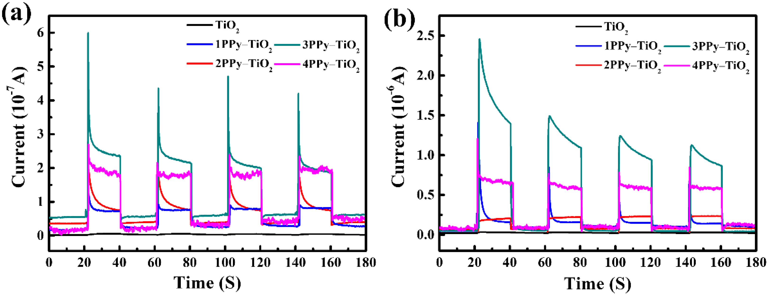
3.2. UV Photo-Detection Properties of the FTO-nPPy-TiO2-FTO Devices

FTO-TiO2-FTO and FTO-nPPy-TiO2-FTO devices were fabricated to investigate the UV photo-detection properties. Figure 6 show the I-t curves detected with different UV light illuminations, where FTO-nPPy-TiO2-FTO devices presented enhanced photocurrent responses while the FTO-TiO2-FTO device showed almost no photocurrent, suggesting that the deposition of PPy film promoted the UV photo-detection property of TiO2. The photocurrent would immediately increase when FTO-nPPy-TiO2-FTO devices were irradiated with UV light. In particular, the FTO-3PPy-TiO2-FTO device exhibited the strongest photocurrent due to the proper thickness of PPy film. The FTO-3PPy-TiO2-FTO device had a maximum photocurrent of 6.0 × 10⁻⁷ A at 254 nm irradiation and 2.5 × 10⁻⁶ A at 365 nm irradiation, which was superior to the maximum photocurrent of 2.7 × 10⁻⁷ A at 254 nm irradiation and 1.4 × 10⁻⁶ A at 365 nm irradiation of the FTO-4PPy-TiO2-FTO device, the maximum photocurrent of 1.0 × 10⁻⁷ A at 254 nm irradiation and 0.8 × 10⁻⁶ A at 365 nm irradiation of the FTO-1PPy-TiO2-FTO device, and the maximum photocurrent of 2.0 × 10⁻⁷ A at 254 nm irradiation and 0.2 × 10⁻⁶ A at 365 nm irradiation of the FTO-2PPy-TiO2-FTO device. The I-V curves measured at dark and different UV light illuminations of the FTO-3PPy-TiO2-FTO device in Figure S2 showed a rectifier phenomenon induced by a p–n heterojunction. Furthermore, the FTO-3PPy-TiO2-FTO device had the highest current under 365 nm wavelength UV light. In fact, under UV light, photoelectrons might be efficiently inserted in the TiO2 conduction band and subsequently into PPy, which accelerated the separation of photogenerated charges and led to the high photocurrent of the FTO-3PPy-TiO2-FTO device. By comparing Figure 6a,b, it was found that the photocurrent when UV light was irradiated at 365 nm was higher than that at 254 nm, indicating that the assembled device should hold great promise as a UV-detector at 365 nm. Accordingly, the FTO-3PPy-TiO2-FTO device exhibited good performance with sensitivity of 41.7, responsivity of 3.5 × 10⁻³ A/W, and detectivity of 2.1 × 10¹² Jones, which outperforms the TiO2-based devices in previous literature as shown in Table S1.
Electrochemical impedance spectroscopy (EIS) was further carried out to study the interfacial charge transfer dynamics of the fabricated FTO-nPPy-TiO2-FTO devices. As can be seen from the Nyquist plots in Figure 7, well-defined semi-circles that reflected the charge transfer resistance were observed. The diameters of the semi-circles were sorted as follows: 1PPy-TiO2 > 2PPy-TiO2 > 4PPy-TiO2 > 3PPy-TiO2, which was consistent with the order of photocurrent magnitude. Notably, the FTO-3PPy-TiO2-FTO device had the smallest semi-circle among the four devices, denoting the lowest interfacial charge transfer resistance between PPy and TiO2 [37]. This might stem from the strong interaction between PPy film and TiO2 nanorod arrays, which greatly enhanced the optoelectronic properties of 3PPy-TiO2. In addition, the results of this study show that there was a certain correlation between the interface conductivity and the thickness of the PPy layer in the PPy-TiO2 semiconductor composite; too small or too large thickness was not conducive to the improvement of its conductivity. Furthermore, the sample of 3PPy-TiO2 had the best electrical conductivity, which was also one of the important reasons for its best photoelectric response performance.
Based on the above results and discussion, the formation mechanism of photoelectric response and the built-in electric field of the p-n junction of PPy-TiO2 are shown in Figure 8. The dominated holes were easily lost in the p-type semiconductor of PPy, so the Fermi level (EF) was close to the valence band (EV). Similarly, in the n-type semiconductor of TiO2, electrons were dominant, and they were easily lost, so the Fermi level was close to the conduction band (EC). PPy was in close contact with the TiO2 interface, and a p-n junction was formed at the interface to form a built-in electric field, as shown in Figure 8c. The built-in electric field at equilibrium caused the energy band to bend so that the Fermi levels of the two types of semiconductors were at the same level, and there was no net current flow in the semiconductors. Figure 8a,b show the schematic diagram of the photoelectric response. When UV light was irradiated on PPy-TiO2, photogenerated electron-hole pairs were excited in TiO2, electrons were excited from the valence band of TiO2 to the conduction band, and the presence of a built-in electric field effectively separated photogenerated electron-hole pairs to form a net current so that inspection signals could be collected. It can be seen from the mechanism diagram that the photocurrent was closely related to the light response nature of the photosensitive material itself and the strength of the built-in electric field. Improving the photoresponse performance of the UV detector can be achieved by improving the photoresponse properties of the photosensitive material itself, such as surface doping modification. In addition, the performance of the UV photodetector can be improved by enhancing the strength of the built-in electric field at the interface of the composite. The results show that there was a certain relationship between the intensity of the electric field and the thickness of the semiconductor layer. That is, the thickness of the semiconductor layer had an optimal value. When the thickness of PPy is too small, the built-in electric field formed is weak, and when the thickness of PPy is too large, the conductivity may be weakened.

4. Conclusions

In summary, the TiO2 nanorod arrays were successfully prepared by a simple hydrothermal method. Additionally, a PPy film deposited-TiO2 nanorod arrays was constructed by simple in situ oxidative polymerization, and the nanocomposites served as materials for UV photodetectors. The thickness of the PPy layer in PPy-TiO2 composite material can be effectively regulated by the deposition times. Additionally, the thickness of the PPy layer can be effectively controlled around 20 nm~200 nm. Furthermore, there was a strong interaction between the TiO2 nanorod arrays film and the PPy layer. Additionally, a p-n junction formed between PPy and TiO2, which inhibited the recombination of photogenerated carriers in TiO2, leading to better UV photo-detection performance of PPy-TiO2 than pure TiO2 nanorod arrays. The photodetectors fabricated with 3PPy-TiO2 showed the best performance with a sensitivity of 41.7 and responsivity of 3.5 × 10⁻³ A/W, which was mainly due to their excellent electrical conductivity. This work provides a facile method to prepare TiO2-based nanocomposites for UV photodetectors and is expected to be extended to other fields, including electrochemical storage and microwave-absorbing.

Supplementary Materials

The following supporting information can be downloaded at: https://www.mdpi.com/article/10.3390/chemosensors10070277/s1, Figure S1: TEM image (a) of TiO2 and SEM image (b) of TiO2-FTO film. Figure S2: The I-V curves of the FTO-3PPy-TiO2-FTO device. Table S1: The comparison of results between previous reported PDs and our devices [20,38,39,40,41].

Author Contributions

Conceptualization, H.W. and P.Q.; formal analysis, H.W.; investigation, P.Q.; data curation, H.W. and P.Q.; writing—original draft preparation, H.W., H.-L.S. and H.-X.W.; writing—review and editing, B.-K.L. and Y.-B.X.; visualization, H.-L.S.; supervision, Y.-H.F. and W.W.; project administration, Y.-H.F. and W.W.; funding acquisition, H.W., Y.-H.F. and W.W. All authors have read and agreed to the published version of the manuscript.

Funding

This research was funded by the National Natural Science Foundation of China (NSFC) (No. 21908071, 22174027, 52001080), the Natural Science Foundation of Guangdong (No. 2020A1515011319), the Research Fund Program of Guangdong Provincial Key Lab of Green Chemical Product Technology (No. GC202107), the Joint Research Institute Fund of Guangzhou University and Guangdong Institute of Corrosion Science and Technology Innovation (20210209), the Key Laboratory of Pulp and Paper Science and Technology of Ministry of Education of China (No. KF201902), Natural Science Foundation of Shandong Province (ZR2020QB197), CAS Key Laboratory of Renewable Energy (No. E129kf0301). We thank Long-Wen Chen for the original draft preparation.

Institutional Review Board Statement

Not applicable.

Informed Consent Statement

Not applicable.

Data Availability Statement

Not applicable.

Conflicts of Interest

The authors declare no conflict of interest.

References

  1. Chen, J.; Ouyang, W.; Yang, W.; He, J.; Fang, X. Recent Progress of Heterojunction Ultraviolet Photodetectors: Materials, Integrations, and Applications. Adv. Funct. Mater. 2020, 30, 1909909. [Google Scholar] [CrossRef]
  2. Ma, H.; Zhang, H.; Fang, J.; Liu, X.; Wang, S.; Xie, M. Fabrication of Au-Cu Ordered Metallic Nanoparticle Arrays and Their Optical Properties. Chin. J. Rare Met. 2020, 44, 916–926. [Google Scholar]
  3. Li, S.; Deng, T.; Zhang, Y.; Li, Y.; Yin, W.; Chen, Q.; Liu, Z. Solar-blind ultraviolet detection based on TiO2 nanoparticles decorated graphene field-effect transistors. Nanophotonics 2019, 8, 899–908. [Google Scholar] [CrossRef]
  4. Yang, T.; Chen, S.; Li, X.; Xu, X.; Gao, F.; Wang, L.; Chen, J.; Yang, W.; Hou, X.; Fang, X. High-Performance SiC Nanobelt Photodetectors with Long-Term Stability against 300 °C up to 180 Days. Adv. Funct. Mater. 2019, 29, 1806250. [Google Scholar] [CrossRef]
  5. Li, X.; Ma, H.; Wang, X.; Chen, F.; Zeng, X. Structural and Luminescent Properties of Eu, Mg Co-doped GaN. Chin. J. Rare Met. 2020, 44, 1170–1176. [Google Scholar]
  6. Zheng, K.-G.; Yang, T.-Y.; Guo, Z. Porous Pb-Doped ZnO Nanobelts with Enriched Oxygen Vacancies: Preparation and Their Chemiresistive Sensing Performance. Chemosensors 2022, 10, 96. [Google Scholar] [CrossRef]
  7. Nguyen, T.; Patel, M.; Kim, S.-H.; Mir, R.; Yi, J.-S.; Dao, V.-A.; Kim, J.-D. Transparent photovoltaic cells and self-powered photodetectors by TiO2/NiO heterojunction. J. Power Sources 2021, 481, 228865. [Google Scholar] [CrossRef]
  8. Wang, H.; Qin, P.; Yi, G.; Zu, X.; Zhang, L.; Hong, W.; Chen, X. A high-sensitive ultraviolet photodetector composed of double-layered TiO2 nanostructure and Au nanoparticles film based on Schottky junction. Mater. Chem. Phys. 2017, 194, 42–48. [Google Scholar] [CrossRef]
  9. Zheng, W.; Dong, Y.; Li, T.; Chen, J.; Chen, X.; Dai, Y.; He, G. MgO blocking layer induced highly UV responsive TiO2 nanoparticles based self-powered photodetectors. J. Alloys Compd. 2021, 869, 159299. [Google Scholar] [CrossRef]
  10. Tian, A.; Shi, X.; Tan, H.; Li, B.; Ma, J.; Yang, H. Preparation and Photocatalytic Properties of Ni Doped TiO2 Nanotube. Chin. J. Rare Met. 2021, 45, 41–46. [Google Scholar]
  11. Haidry, A.; Fatima, Q.; Mehmood, A.; Shahzad, A.; Ji, Y.; Saruhan, B. Adsorption Kinetics of NO2 Gas on Pt/Cr-TiO2/Pt-Based Sensors. Chemosensors 2022, 10, 11. [Google Scholar] [CrossRef]
  12. Zhang, D.; Liu, C.; Yin, B.; Xu, R.; Zhou, J.; Zhang, X.; Ruan, S. Organics filled one-dimensional TiO2 nanowires array ultraviolet detector with enhanced photo-conductivity and dark-resistivity. Nanoscale 2017, 9, 9095–9103. [Google Scholar] [CrossRef] [PubMed]
  13. Zheng, X.; Sun, Y.; Qin, H.; Ji, Z.; Chi, H. Interface engineering on ZnO/Au based Schottky junction for enhanced photoresponse of UV detector with TiO2 inserting layer. J. Alloys Compd. 2020, 816, 152537. [Google Scholar] [CrossRef]
  14. Ouyang, W.; Teng, F.; Fang, X. High Performance BiOCl Nanosheets/TiO2 Nanotube Arrays Heterojunction UV Photodetector: The Influences of Self-Induced Inner Electric Fields in the BiOCl Nanosheets. Adv. Funct. Mater. 2018, 28, 1707178. [Google Scholar] [CrossRef]
  15. Yang, D.; Du, F.; Ren, Y.; Kang, T.; Hu, P.; Teng, F.; Fan, H. A high-performance NiO/TiO2 UV photodetector: The influence of the NiO layer position. J. Mater. Chem. C 2021, 9, 14146–14153. [Google Scholar] [CrossRef]
  16. Wang, Y.; Chen, L.; Zhou, H.; Wei, K.; Zhu, Z.; Xie, E.; Cao, W.; Han, W. Rutile TiO2 nanowire arrays interconnected with ZnO nanosheets for high performance electrochemical UV sensors. J. Mater. Chem. C 2019, 7, 8011–8018. [Google Scholar] [CrossRef]
  17. Mojtabavi, E.A.; Nasirian, S. Flexible self-powered ultraviolet-visible photodetector based on polyaniline-titanium dioxide heterostructures: The study of the rearrangement of layers. Appl. Surf. Sci. 2019, 492, 189–198. [Google Scholar] [CrossRef]
  18. Mojtabavi, E.A.; Nasirian, S. A self-powered UV photodetector based on polyaniline/titania nanocomposite with long-term stability. Opt. Mater. 2019, 94, 28–34. [Google Scholar] [CrossRef]
  19. Zhang, H.; Abdiryim, T.; Jamal, R.; Li, J.; Liu, H.; Kadir, A.; Zou, D.; Che, Y.; Serkjan, N. Self-powered TiO2 NRs UV photodetectors: Heterojunction with PTTh and enhanced responsivity by Au nanoparticles. J. Alloys Compd. 2022, 899, 163279. [Google Scholar] [CrossRef]
  20. Che, Y.; Zhang, H.; Abdiryim, T.; Jamal, R.; Kadir, A.; Helil, Z.; Liu, H. Ultraviolet photodetectors based on TiO2 nanorod arrays/PEDOT-type conducting polymers. Opt. Mater. 2021, 122, 111805. [Google Scholar] [CrossRef]
  21. Kareem, O.A.; Mohameed, S.J.; Ibrahim, I.M. The importance of doping TiO2 into polypyrrol nanofibers to improve their optical sensitivity. J. Phys. Conf. Ser. 2021, 2114, 012057. [Google Scholar] [CrossRef]
  22. Qin, P.; Yi, G.; Zu, X.; Wang, H.; Tan, M.; Luo, H. Preparation of graphene-TiO2 nanocomposite films and its photocatalytic performances on degradation of Rhodamine B. Pigm. Resin Technol. 2018, 47, 79–85. [Google Scholar] [CrossRef]
  23. Li, S.; Yin, W.; Li, Y.; Sun, J.; Zhu, M.; Liu, Z.; Deng, T. High sensitivity ultraviolet detection based on three-dimensional graphene field effect transistors decorated with TiO2 NPs. Nanoscale 2019, 11, 14912–14920. [Google Scholar] [CrossRef] [PubMed]
  24. Gao, Y.; Xu, J.; Shi, S.; Dong, H.; Cheng, Y.; Wei, C.; Zhang, X.; Yin, S.; Li, L. TiO2 Nanorod Arrays Based Self-Powered UV Photodetector: Heterojunction with NiO Nanoflakes and Enhanced UV Photoresponse. ACS Appl. Mater. Interfaces 2018, 10, 11269–11279. [Google Scholar] [CrossRef] [PubMed]
  25. Liao, Z.; Ma, M.; Tong, Z.; Wang, R.; Bi, Y.; Chen, Y.; Chung, K.-L.; Ma, Y. Fabrication of ZnFe2O4/C@PPy composites with efficient electromagnetic wave absorption properties. J. Colloid Interf. Sci. 2021, 602, 602–611. [Google Scholar] [CrossRef] [PubMed]
  26. Bi, Y.; Ma, M.; Liu, Y.; Tong, Z.; Wang, R.; Chung, K.-L.; Ma, A.; Wu, G.; Ma, Y.; He, C.; et al. Microwave absorption enhancement of 2-dimensional CoZn/C@ MoS2@ PPy composites derived from metal-organic framework. J. Colloid Interf. Sci. 2021, 600, 209–218. [Google Scholar] [CrossRef]
  27. He, N.; Yang, X.; Shi, L.; Yang, X.; Lu, Y.; Tong, G.; Wu, W. Chemical conversion of Cu2O/PPy core-shell nanowires (CSNWs): A surface/interface adjustment method for high-quality Cu/Fe/C and Cu/Fe3O4/C CSNWs with superior microwave absorption capabilities. Carbon 2020, 166, 205–217. [Google Scholar] [CrossRef]
  28. Zhao, D.; Dai, M.; Zhao, Y.; Liu, H.; Liu, Y.; Wu, X. Improving electrocatalytic activities of FeCo2O4@FeCo2S4@PPy electrodes by surface/interface regulation. Nano Energy 2020, 72, 104715. [Google Scholar] [CrossRef]
  29. Bi, Y.; Ma, M.; Liao, Z.; Tong, Z.; Chen, Y.; Wang, R.; Ma, Y.; Wu, G. One-dimensional Ni@Co/C@PPy composites for superior electromagnetic wave absorption. J. Colloid Interface Sci. 2022, 605, 483–492. [Google Scholar] [CrossRef]
  30. Ding, J.; Wang, L.; Zhao, Y.; Xing, L.; Yu, X.; Chen, G.; Zhang, J.; Che, R. Boosted interfacial polarization from multishell TiO2@ Fe3O4@ PPy heterojunction for enhanced microwave absorption. Small 2019, 15, 1902885. [Google Scholar] [CrossRef]
  31. Yan, S.; Li, Y.; Xie, F.; Wu, J.; Jia, X.; Yang, J.; Song, H.; Zhang, Z. Environmentally safe and porous MS@TiO2@PPy monoliths with superior visible-light photocatalytic properties for rapid oil–water separation and water purification. ACS Sustain. Chem. Eng. 2020, 8, 5347–5359. [Google Scholar] [CrossRef]
  32. Ha, J.-U.; Lee, J.; Abbas, M.-A.; Lee, M.-D.; Lee, J.; Bang, J.-H. Designing hierarchical assembly of carbon-coated TiO2 nanocrystals and unraveling the role of TiO2/carbon interface in lithium-ion storage in TiO2. ACS Appl. Mater. Interfaces 2019, 11, 11391–11402. [Google Scholar] [CrossRef] [PubMed]
  33. Li, Z.-L.; Li, Z.-Q.; Zuo, C.; Fang, X. Application of Nanostructured TiO2 in UV Photodetectors: A Review. Adv. Mater. 2022, 2109083. [Google Scholar] [CrossRef] [PubMed]
  34. Tang, H.; Berger, H.; Schmid, P.; Lévy, F.; Burri, G. Photoluminescence in TiO2 anatase single crystals. Solid State Commun. 1993, 87, 847–850. [Google Scholar] [CrossRef]
  35. Maurya, A.; Chauhan, P.; Mishra, S.K.; Srivastava, R.K. Structural, optical and charge transport study of rutile TiO2 nanocrystals at two calcination temperatures. J. Alloys Compd. 2011, 509, 8433–8440. [Google Scholar] [CrossRef]
  36. Serpone, N.; Lawless, D.; Khairutdinov, R. Size effects on the photophysical properties of colloidal anatase TiO2 particles: Size quantization versus direct transitions in this indirect semiconductor? J. Phys. Chem. 1995, 99, 16646–16654. [Google Scholar] [CrossRef]
  37. Hsu, C.-P.; Lee, K.-M.; Huang, J.T.-W.; Lin, C.-Y.; Lee, C.-H.; Wang, L.-P.; Tsai, S.-Y.; Ho, K.-C. EIS analysis on low temperature fabrication of TiO2 porous films for dye-sensitized solar cells. Electrochim. Acta 2008, 53, 7514–7522. [Google Scholar] [CrossRef]
  38. Zheng, L.; Yu, P.; Hu, K.; Teng, F.; Chen, H.; Fang, X. Scalable-production, self-powered TiO2 nanowell–organic hybrid UV photodetectors with tunable performances. ACS Appl. Mater. Interfaces 2016, 8, 33924–33932. [Google Scholar] [CrossRef]
  39. Zheng, L.; Deng, X.; Wang, Y.; Chen, J.; Fang, X.; Wang, L.; Shi, X.; Zheng, H. Self-powered flexible TiO2 fibrous photodetectors: Heterojunction with P3HT and boosted responsivity and selectivity by Au nanoparticles. Adv. Funct. Mater. 2020, 30, 2001604. [Google Scholar] [CrossRef]
  40. Chen, D.; Wei, L.; Meng, L.; Wang, D.; Chen, Y.; Tian, Y.; Yan, S.; Mei, L.; Jiao, J. High-performance self-powered UV detector based on SnO2-TiO2 nanomace arrays. Nanoscale Res. Lett. 2018, 13, 92. [Google Scholar] [CrossRef] [Green Version]
  41. Zhou, M.; Wu, B.; Zhang, X.; Cao, S.; Ma, P.; Wang, K.; Fan, Z.; Su, M. Preparation and UV photoelectric properties of aligned ZnO–TiO2 and TiO2–ZnO core–shell structured heterojunction nanotubes. ACS Appl. Mater. Interfaces 2020, 12, 38490–38498. [Google Scholar] [CrossRef] [PubMed]
Figure 1. Schematic diagram of the fabrication of the FTO-nPPy-TiO2-FTO device.
Chemosensors 10 00277 g001
Figure 2. Cross-sectional SEM images of PPy-TiO2 nanocomposites prepared by different deposition times, (a) 1PPy-TiO2, (b) 2PPy-TiO2, (c) 3PPy-TiO2, and (d) 4PPy-TiO2.
Chemosensors 10 00277 g002
Figure 3. TEM images (a,b), HRTEM image (c), and the corresponding selected area electron diffraction pattern (d), STEM image (e), and the corresponding elemental mapping images (fi) of 3PPy-TiO2.
Chemosensors 10 00277 g003
Figure 4. Raman spectra (a) and XRD patterns (b) of pure TiO2 and nPPy-TiO2 nanocomposites prepared by different deposition times; XPS surveys (c) and high-resolution Ti2p spectra (d) of pure TiO2 and 3PPy-TiO2.
Chemosensors 10 00277 g004
Figure 5. UV-Vis absorption spectra (a) and photoluminescence spectrum (b) of pure TiO2 and nPPy-TiO2 nanocomposites prepared by different deposition times.
Chemosensors 10 00277 g005
Figure 6. I-t curves of FTO-TiO2-FTO and FTO-nPPy-TiO2-FTO devices prepared by different deposition times with 254 nm ((a), 500 μW/cm2) and 365 nm ((b), 470 μW/cm2) UV light illumination.
Chemosensors 10 00277 g006
Figure 7. Nyquist plots of FTO-nPPy-TiO2-FTO devices prepared by different deposition times with 254 nm (a) and 365 nm (b) UV light illumination.
Chemosensors 10 00277 g007
Figure 8. Schematic diagram of photoelectric response (a,b) and the formation mechanism of the built-in electric field of the p-n junction in PPy-TiO2 composites (c).
Chemosensors 10 00277 g008
Publisher’s Note: MDPI stays neutral with regard to jurisdictional claims in published maps and institutional affiliations.

