Article

Surface-Catalyzed Zinc Oxide Nanorods and Interconnected Tetrapods as Efficient Methane Gas Sensing Platforms

Department of Materials Science and Engineering, Pennsylvania State University, University Park, PA 16802, USA
*
Authors to whom correspondence should be addressed.
Chemosensors 2023, 11(9), 506; https://doi.org/10.3390/chemosensors11090506
Submission received: 11 August 2023 / Revised: 9 September 2023 / Accepted: 12 September 2023 / Published: 17 September 2023
(This article belongs to the Special Issue The State-of-the-Art Gas Sensor)

Abstract

:
Nanostructured metal oxide semiconductors have proven to be promising for the gas sensing domain. However, there are challenges associated with the fabrication of high-performance, low-to-room-temperature operation sensors for methane and other gases, including hydrogen sulfide, carbon dioxide, and ammonia. The functional properties of these semiconducting oxides can be improved by altering the morphology, crystal size, shape, and topology. Zinc oxide (ZnO) is an attractive option for gas sensing, but the need for elevated operating temperatures has limited its practical use as a commercial gas sensor. In this work, we prepared ZnO nanorod (ZnO-NR) arrays and interconnected tetrapod ZnO (T-ZnO) network sensing platforms as chemiresistive methane sensors on silicon substrates with platinum interdigitated electrodes and systematically characterized their methane sensing response in addition to their structural and physical properties. We also conducted surface modification by photochemical-catalyzed palladium, Pd, and Pd-Ag alloy nanoparticles and compared the uniformly distributed Pd decoration versus arrayed dots. The sensing performance was assessed in terms of target gas response magnitude (RM) and response percentage (R) recorded by changes in electrical resistance upon exposure to varying methane concentration (100–10,000 ppm) under thermal (operating temperatures = 175, 200, 230 °C) and optical (UV A, 365 nm illumination) excitations alongside response/recovery times, and limit of detection quantification. Thin film sensing platforms based on T-ZnO exhibited the highest response at 200 °C (RM = 2.98; R = 66.4%) compared to ZnO-NR thin films at 230 °C (RM = 1.34; R = 25.5%), attributed to the interconnected network and effective bandgap and barrier height reduction of the T-ZnO. The Pd-Ag-catalyzed and Pd dot-catalyzed T-ZnO films had the fastest response and recovery rates at 200 °C and room temperature under UV excitation, due to the localized Pd nanoparticles dots resulting in nano Schottky barrier formation, as opposed to the films coated with uniformly distributed Pd nanoparticles. The experimental findings present morphological differences, identify various mechanistic aspects, and discern chemical pathways for methane sensing.

Graphical Abstract

1. Introduction

There has been growing interest in the development of state-of-the-art gas sensors to monitor toxic, hazardous, and greenhouse gas emissions (GHG), including methane (CH4) and carbon dioxide (CO2). One of the main contributors to these emissions, other than modern industries, is agricultural livestock, specifically, ruminants, i.e., cattle, sheep, etc. Ruminants produce GHG as a byproduct of digestion and microbial fermentation occurring in their second stomach compartment, the rumen, to convert their feed into usable forms of energy [1,2]. Ruminants are responsible for approximately 27% of the total CH4 gas emissions produced in the United States, according to a study conducted by the Environmental Protection Agency (EPA) [1,3]. Typically, CH4 gas traps heat from the sun and warms the Earth’s atmosphere, contributing to global warming and climate change [4]. The demand for agricultural products is projected to increase by ~70% by 2050 due to higher standards of living and the increasing global population [5]. A review of GHG sensors by Santhanam et al., reported the development of a specific chemo-resistive CH4 sensor using multiwalled carbon nanotubes/metal oxide composites [4]. Also, Rezaeipour et al., detail the comparison of nanoparticle and nanorod morphologies of nickel ferrite (Fe2NiO4) as sensors for volatile organic compounds, another gas contributing to global climate change [6]. Nevertheless, metal oxide semiconducting gas sensors have shown enormous potential and prove to be quite versatile due to varied morphologies, topologies, and rich surface catalytic chemistry.
Nanostructured metal oxide semiconductors (MOSs) have the potential to play a critical role in gas sensing applications due to their interconnected nanograins, large surface area, and shorter diffusion length along with their ease of fabrication, low manufacturing costs and ability to detect multiple different gases [7]. Moreover, the ubiquitous porosity in MOSs can enhance gas/air diffusion through improved accessibility to nanograins and reactive sites [8]. However, their disadvantages have been major limitations in their use as widespread commercial gas sensors, which include cross-selectivity, baseline resistance drift, and high operating temperatures [9]. Semiconducting oxides (e.g., ZnO, SnO2 [10]) with a d10 electronic configuration witnessed enormous attention in the fabrication of practical micro- and nanodevices for gas sensing applications. Specifically, for ZnO, the porosity of various morphologies is known to play a significant role in overall sensor performance in addition to device architectures [11]. To address the need for the decreased operating temperature of ZnO-based gas sensors, in this study, we investigated two morphologies, namely one-dimensional (1D) vertically standing nanorods and three-dimensional (3D) tetrapods, with surface-catalyzed modification strategies. Different material catalysts studied include noble metals (i.e., Pd, Au, and Pt) to promote oxidative reactions with CH4 at lower temperatures [12,13]. Palladium (Pd) has been effectively used as a catalyst for various ZnO thin film morphologies, such as interconnected nanoparticles, nanosheets, nanorods and nanoplates [14,15,16,17]. The operating temperature of the ZnO film plays a significant role in the adsorption/desorption of the methane (CH4), as the adsorbed oxygen species at elevated temperatures (O) are more reactive than those generated at lower temperatures (O2) (T ≤ 100 °C) [18,19]. In addition to thermal excitation and surface modification, UV illumination that has photon energy higher than the bandgap energy of ZnO (3.37 eV), has also been reported as a surface catalyst due to the generation of electron-hole (e–h) pairs. Ref. [20] Fan et al., reported UV-activated ZnO sensors that responded to H2 gas, crediting continuous UV illumination for improving sensitivity and overcoming long-term drift due to the high reactivity of the photogenerated oxygen ions [O2(hν)] with the target gas. A thickness-dependence study on ZnO films under UV illumination conducted by Su et al. demonstrated the highest sensitivity at ambient temperature and found that response to the target gas (NO2) increased with increasing thickness to a maximum of 1500 nm, after which the response began decreasing [21,22]. While this study highlights the significance of UV for lowering operating temperature, the thicker films possessed higher porosity which had a larger penetration depth for the UV light to create more photogenerated carriers and efficient diffusion of gas molecules [17]. This study examines, at a fundamental level, the hierarchical morphology-promoted enhancement of methane sensing from vertically aligned nanorod and networked tetrapod ZnO films, surface catalysts, and thermal and UV excitation, providing a thorough physical and chemical understanding of sensing mechanism.

2. Materials and Methods

2.1. Preparation of ZnO-NR Array Thin Films

ZnO nanorod (ZnO-NR) thin films were prepared via the aqueous phase chemical solution growth method [16,17]. Briefly, a 25 mM zinc acetate in ethanol seed solution was prepared with 40 wt.% Au nanoparticles. Spin coating of seed solution was performed at 2000 rpm for 20 s and repeated eight times to obtain certain thickness of approximately 120 nm onto commercial p-type <100> Si substrates of 1 × 2 cm2 dimension cleaned with acetone and prefabricated Pt interdigitated electrodes (IDE) via a dry etch and lift-off process of 200 μm finger width and 200 μm spacing. Samples were placed in a hot place set at 60 °C between layers for better crystallization. Following spin coating, samples were annealed at 350 °C for 30 min to complete the seed layer. The ZnO-NR growth solution was prepared by mixing equal volumes of 50 mM hexamethylenetetramine (HMT) and 50 mM zinc nitrate (Zn (NO3)2) solutions which were stirred for 15 min prior to growth. Once the zinc acetate seed layer was deposited, samples were placed vertically in sealed containers containing the ZnO growth solution of effective 25 mM concentration in a furnace set at 86 °C for 8 h. Once removed from the furnace, samples were washed to remove excess debris with isopropyl alcohol (IPA) followed by deionized (DI) water and dried prior to characterization and testing. Scheme 1a summarizes ZnO-NR synthesis and Pd decoration for subsequent characterization and testing.

2.2. Preparation of Interconnected T-ZnO Films

Tetrapod ZnO (T-ZnO) powder was prepared via direct flame transport synthesis (FTS) method utilizing zinc nanoparticles with an average particle size of 40–60 nm and polyvinyl butyral (PVB) precursors [23,24,25]. T-ZnO powder was dispersed in a dimethyl sulfoxide (DMSO) solution containing 2 wt.% PVB to achieve a 3 wt.% T-ZnO solution. The solution was drop-casted onto cleaned p-type <100> Si substrates (1 × 1.5 cm2) with Pt IDE previously described. The samples were then dried at 60 °C for 8 h to evaporate excess solution. Pd nanoparticles were deposited on the ZnO-NR and T-ZnO sensing films.
The Pd nanoparticles were synthesized from a solution composed of palladium chloride (PdCl2) and polyvinylpyrrolidone (PVP) in methanol with a molar ratio of 0.25 mM Pd: 0.01 mM PVP. A small quantity of the Pd solution (40–60 μL) was used to coat the ZnO-NR (Pdcat/ZnO-NR) and T-ZnO (Pdcat/T-ZnO) films which were subsequently cured under UV light (λ = 365 nm) and annealed at 400 °C for 30 min to remove polymeric residue and promote Pd nanoparticle crystallization. All the chemicals were purchased from Sigma-Aldrich and were used without further purification.

2.3. Morphological Characterization and Methane Sensing Measurements

All samples were characterized using X-ray diffraction, XRD (Pan Analytical Empyrean III), field emission scanning electron microscopy (FESEM), transmission electron microscopy (TEM) and energy dispersive X-ray spectroscopy (EDX) (FEI Apreo S) to determine crystallinity, surface morphology at micro to nanoscale, and elemental distribution, respectively. The TEM and high-angle annular dark-field scanning transmission electron microscopy (HAADF-STEM) imaging was conducted using a Thermo Fisher Talos F200X operated at 200 kV. The EDS data and elemental maps were collected in STEM mode. XRD was performed with a CuKα radiation source (λ = 1.5405 Å) in 2θ range of 30–60° operating at 40 kV and 40 mA. Optical properties, such as UV-visible absorption spectroscopy (Hitachi UH4150) and room temperature photoluminescence (PL) spectroscopy (Edinburgh Instruments FLS1000) were also investigated.
The ZnO-NR and T-ZnO films were evaluated for CH4 sensing with contacts fabricated on a junction of an IDE finger and bar on either side of the Pt IDE on Si substrates. Conductive silver ink with a resistivity of 5–6 µΩ cm (Sigma Aldrich, St. Louis, MO, USA) was used to attach Cu wire with a diameter of 0.125 mm for electrical measurements. A Keithley 2401 electrometer with the Kickstart Digital Multimeter software was utilized to measure the current-voltage (I–V) curves and sensing responses in the dark and under UV illumination at λ = 365 nm (Analytik Jena UVP 3UV Lamp), at various temperatures and as a function of methane concentration. The response magnitude (RM) and response and recovery times of the films were determined from resistance measurements using a Keithley 6514 electrometer and the afore mentioned Kickstart Digital Multimeter software. A custom-made gas sensing chamber was designed to quantify the sensors’ response as a function of methane concentration mixed with synthetic dry air, illustrated in Scheme 1b. Response magnitude was calculated following R M = R a / R g , where Ra is the resistance in air and Rg is the resistance in methane. Response percentage/percentile was determined from R % = ( R a R g ) / R g × 100 . The sensitivity, S, or limit of detection (LOD) was derived from the slope of the calibration curve (sensor response versus target gas concentration) [11,26]. Each gas cylinder was connected to a mass flow controller (MFC) (Omega Engineering Inc.) to control the mixing of the two gases and the resulting concentration of methane flowed into the chamber. A ceramic heater was connected to a power supply and calibrated to study the effect of temperature on sensor response in dark (OFF) and under UV A illumination (ON) in the gas sensing chamber.

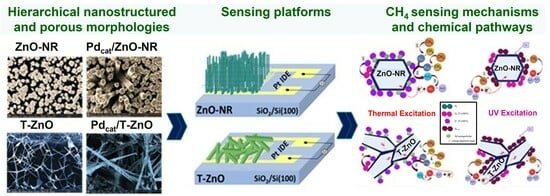
3. Results and Discussion

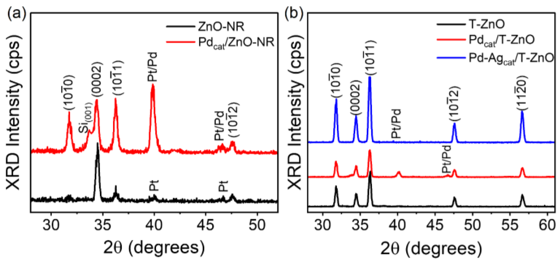
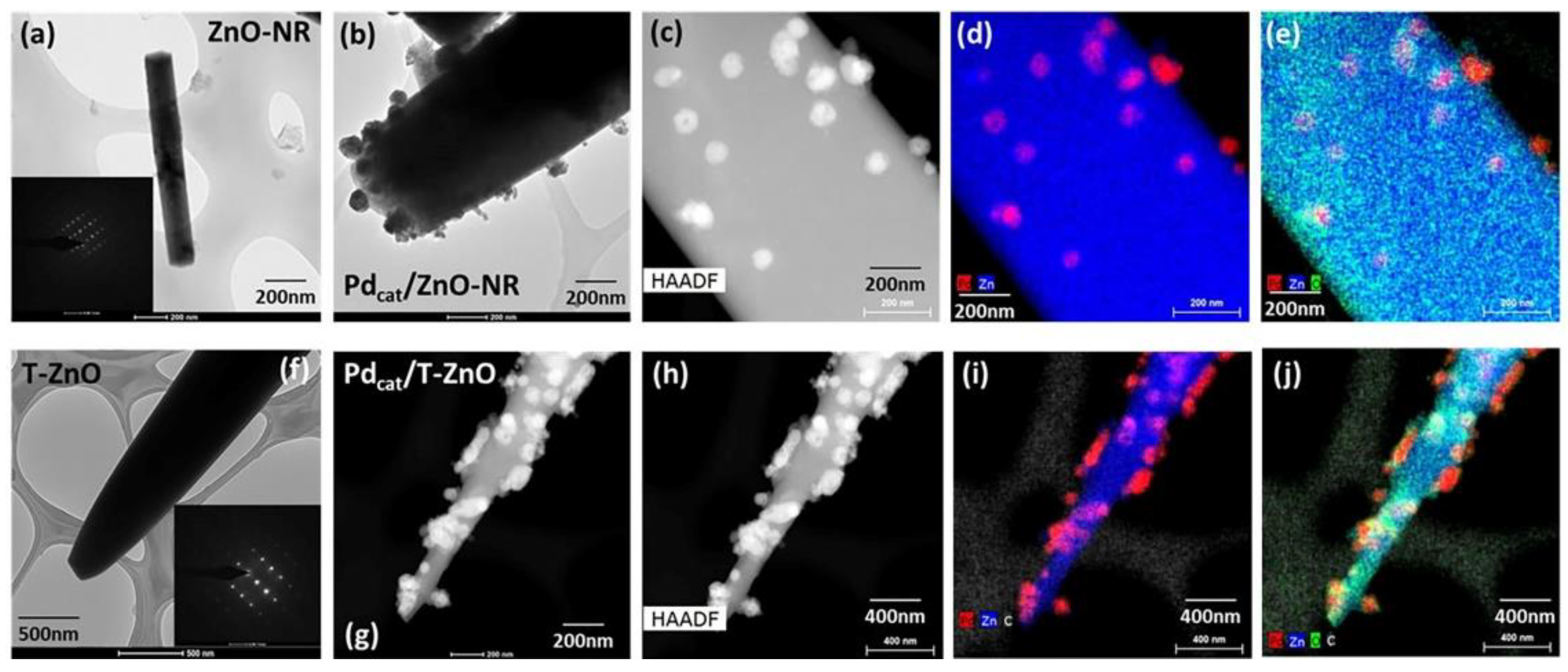
3.1. Structural, Optical, and Electrical Properties Characterization

The XRD spectra as shown in Figure 1 exhibited polycrystalline structure for both ZnO-NR and T-ZnO as well as Pd decorated films (Pdcat/ZnO-NR; Pdcat/T-ZnO). The reflection peaks identified at 2θ values of 31.7°, 34.4°, 36.2°, and 47.6° correspond to lattice planes of (100), (002), (101), and (102), respectively, indexed to the hexagonal wurtzite ZnO structure (JCPDS Card No. 79-0206).
The peaks at 2θ values of 39.86° and 46.6° are due to Pt interdigitated electrodes (IDE) and Pd nanoparticles, and can be indexed to the (111) and (200) phases of both the Pd and Pt [27,28,29,30]. The peak corresponding to the (002) plane at θ = 17 . 2 was used to determine the interplanar spacing, d002, from Bragg’s law, n λ = 2 d sin θ , where n  = 1 for first-order diffraction, λ is the X-ray wavelength ( = 1.5405   Å ), and θ is the angle of diffraction [31,32]. The lattice parameters, c   and a , were determined using Equations (1) and (2) [33,34].
d h k l = 4 3 a 2 h 2 + k 2 + h k + l 2 c 2 1 2
c = λ sin θ
The lattice parameters were found to be c = 5.196   and a = 3.00   for ZnO-NR films and c = 5.20   and a = 3.02   for T-ZnO films. For the Pdcat/ZnO-NR and Pdcat/T-ZnO films, the lattice parameters were c = 5.20   and a = 3.03   . The c lattice parameter was consistent with the bulk values, while a lattice parameter and c a hexagonality ratio ( 1.715 ± 0.05 ) was within 7% of the bulk Wurtzite structural values ( c a .   c = 5.206   , a = 3.249   , c a = 1.602 ). The dislocation density was also determined using:
δ = 1 D 2
where D is the average crystallite size [29]. The latter is calculated using the Debye–Scherrer equation following:
D = k λ β h k l cos θ
where k   is a constant equal to 0.89 and β h k l is the full width at half maximum of the corresponding peak [28]. The dislocation density is defined as the length of the dislocation lines per unit volume in the crystal and is representative of the defects related to the intrinsic stacking faults [35]. The dislocation density, δ , was found to be 0.2982 for ZnO-NR, 0.2951 for Pdcat/ZnO-NR, 0.2954 for T-ZnO, 0.2952 for Pdcat/T-ZnO, and 0.2958 for Pd-Agcat/T-ZnO. The calculated lattice strain, ε , for each film was determined from the formula [28]:
ε = β h k l 4 tan θ
The lattice strain for ZnO-NR was ε = 2.299 × 1 0 4 and ε = 5.68 × 1 0 4 for Pdcat/ZnO-NR. The lattice strain for T-ZnO was ε = 4.60 × 1 0 4 , ε = 4.76 × 1 0 4 for Pdcat/T-ZnO, and ε = 4.85 × 1 0 4 for Pd-Agcat/T-ZnO. The lattice parameters, dislocation density and lattice strain for all the films studied are graphically summarized in Figure S1 (see Supplementary Materials). The morphology was revealed using field emission scanning electron microscopy (FE-SEM) and transmission electron microscopy (TEM). SEM micrographs (Figure 2) revealed that ZnO-NR had well-defined hexagonal-shaped rods, in agreement with the XRD spectral analysis. The tetrapod ZnO, T-ZnO, also exhibited hexagonal rod-shaped arms connected with a well-defined core forming a porous network. The SEM micrographs produced during energy dispersive spectroscopy (EDS) also showed that the Pd nanoparticles were uniformly distributed with minimal agglomeration.
The Pd nanoparticles were observed along each facet of the ZnO films. The majority of the Pd nanoparticles on the ZnO-NR films were observed on the hexagonal top facets of the nanorods, while the Pd nanoparticles were evenly dispersed along the arms and the core in the T-ZnO films. The TEM images of ZnO-NR and T-ZnO and corresponding surface-catalyzed films (Pdcat/ZnO-NR and Pdcat/T-ZnO) shown in Figure 3 clearly exhibit the formation of ZnO-NR morphology or ZnO phase corroborated via selected area electron diffraction pattern; SAED (see insets). It consists of discreet diffraction spots, indicative of extremely high crystallinity of the ZnO nanostructures indexed to ZnO phases as well as the Pd nanoparticles phase. Furthermore, close observation of the TEM images shows homogeneity throughout the ZnO nanorod and T-ZnO body and tip. The high-resolution TEM images revealed (0001) and (010) lattice planes of wurtzite ZnO and Pd (111) or PdO (111) with interplanar spacing of 0.5 nm, 0.24 nm, and 0.31 nm, respectively. The HAADF-STEM (High-angle annular dark field and aberration-corrected scanning/transmission electron microscopy) images of Pd-coated ZnO-NR with overlapped elements (Zn, O, Pd) are also shown in Figure 3. The main advantages of HAADF-STEM images over high-resolution transmission electron microscopy (HRTEM) images are coherence and phase contrast changes. The scattered intensity scale is associated with the atomic number, Z, of the elements in the material system [36]. In our case, the difference between the atomic number of the elements Zn (Z = 30) and Pd (Z = 46) makes it possible to observe notable differences in the image contrast.
The optical properties of the ZnO-NR and T-ZnO thin films were studied using UV-visible (UV-Vis) and photoluminescence (PL) spectroscopy at room temperature (Figure 4). ZnO possesses two emission peaks at room temperature, one at 375 nm, and the other between 480 and 560 nm [24,37]. The first emission peak at 375 nm occurs in the UV region and the second emission peak occurs in the green visible region, which is typically broader due to intrinsic defects present in the ZnO-NR and T-ZnO films [28]. The PL spectra for ZnO-NR shows a sharp peak in the UV region at 388 nm, and multiple smaller peaks in the range of 430–500 nm as well as a broad peak at 600 nm. ZnO-NR and T-ZnO films were exposed to UV light prior to measuring their PL and UV-Visible spectra and it was realized that new defect states were introduced after the exposure (Figure 4b,d) which can play a role in the case of sensing performance under UV excitation discussed below.
The UV-treated ZnO-NR (ZnO-NRUV treated) film had a peak at 395 nm and defect-related peaks at 430 nm, 480 nm, 530 nm, and 625 nm, associated with the oxygen vacancy defects (i.e., VO, VO2+) [31]. The Pd-decorated ZnO-NR (Pdcat/ZnO-NR) film had a peak at 386 nm in the UV region and a defect-related peak at 430 nm. The PL spectra for T-ZnO had a peak at 388 nm in the UV region, and a broader peak at 510 nm, corresponding to oxygen vacancy [31]. The UV-treated T-ZnO (T-ZnOUV treated) film had a sharp emission peak in the UV region around 396 nm, and defect-related peaks at 430 nm and 510 nm from defect emissions due to oxygen vacancy [19,20]. The Pd-coated T-ZnO film (Pdcat/T-ZnO) had a UV emission peak at 367 nm, and a defect-related peak at 430 nm, both blue-shifted compared to the T-ZnO and T-ZnOUV treated samples. The peaks at ~395 nm is associated with the UV emission band and result from the recombination of free excitons via an exciton-exciton collision. It was observed that for ZnO-NR films the peak associated with the UV emission band was much stronger than for the T-ZnO films. This peak can be correlated to the length of the nanorods and/or size of the tetrapod arms wherein the longer length(s) produces a reduced UV emission peak and a stronger green emission peak highlighting the presence of defects and displaying subtle differences not reported previously. As shown in Figure 4a, the UV-Vis spectra for ZnO-NR have a peak at 354 nm, for UV-treated ZnO-NR (ZnO-NRUV treated) the peak shifted slightly to 362 nm, and for the Pd-coated ZnO-NR (Pdcat/ZnO-NR) the peak was red-shifted to 368 nm. The UV-Vis spectra for the T-ZnO samples did not exhibit the same trend. The T-ZnO as well as T-ZnOUV treated films had a peak at 366 nm, while the Pdcat/T-ZnO showed a peak that was blue shifted to 360 nm. This is due to the networked arms of the T-ZnO as opposed to vertically aligned nanorods of ZnO-NR, in addition to Pd coating on the tetrapod that aided in the shifting of the peak position, which could improve lower temperature operation. It is reported that charge transfer, if any, due to either doping or surface modification can induce reasonable band bending, adding a local field to improve charge transfer of holes to the surface, beneficial for surface oxidation reactions that occur between ZnO and CH4 molecules [38].
The energy band gap, E g , was also determined for both ZnO-NR and T-ZnO films from Tauc, PL and absorption spectral analysis (see Figure S2, Supplementary Materials). In Tauc plots, E g can be estimated by plotting α h υ 2 as a function of h υ [39,40]. The UV absorption band used to estimate E g , following Tauc relation:
α h ν = B h υ E g n
where α is the optical absorption coefficient determined from the UV-Vis spectra:
α = ln A d
where d is sample thickness, B is a constant, and n is equal to ½ for allowed direct transitions ( n = 2 for allowed indirect transitions). By extrapolating the linear portion of the plot to the x-intercept, E g can be directly determined [35]. The bandgap from the Tauc plots for the ZnO-NR, ZnO-NRUV Treated, and Pdcat/ZnO-NR films were higher than those determined directly from PL spectra. The bandgap estimates for T-ZnO film were comparable from both the Tauc plot and PL spectra, while for T-ZnOUV Treated and Pdcat/T-ZnO films, they were significantly different.
The electrical properties of ZnO-NR and T-ZnO and functionalized films are investigated prior to methane sensing performance with temperature [I-V(T) or R(T)] and under UV A light illumination (ON/OFF) at room temperature in a dry air environment to obtain steady-state electrical behavior as well as to determine optimum operating temperature and other semiconducting parameters. The resistance as a function of temperature is displayed in Figure 5a. The I-V (current-voltage) characteristics with semilogarithmic and linear scale (insets) measured in air at 25 °C, 200 °C (or 230 °C) are displayed in Figure 5b,c and the I-V curves measured at 200 °C or 230 °C temperature with methane exposure are displayed in Figure 5d,e. Qualitatively, as we increase temperature, the resistance gradually decreases (or conductivity increases shown in Figure S3, Supplementary Materials) indicating average energy bandgap narrowing with temperature ranging between 3.37 eV and 3.15 eV as expected for semiconductors determined following Varshni’s model [11,41].
The electrical conductivity ( σ ) was calculated as above and plotted with inverse temperature, 1 T , in dark (OFF) and under UV A illumination and the resultant plots were utilized to determine the defect activation energy ( E a ) that traps carriers causing generation–recombination current [42] for each sensing film (see Figure S3, Supplementary Materials). The activation energy obtained from the linear fit ranged between 0.24 and 0.54 eV for thermal and 0.025 and 0.10 eV for UV activation clearly supporting the latter excitation for reduced power consumption yielding low or room temperature operation for gas sensing devices (see also Table S1, Supplementary Materials).
At a more fundamental level, the current conduction is governed by the thermionic emission of majority carriers over a potential barrier determined by the reverse saturation current ( I s ) for a metal-semiconductor junction or Schottky junction. It becomes important to study this as it is highly dependent on temperature and UV excitation. Following thermionic emission theory, the current formulation is given by [43]:
I = A A T 2 exp q ϕ B k B T exp q V n k B T 1 = I S   exp q V n k B T 1   #
For V > 3 k B T q , where A is the contact area, A the effective Richardson constant ( 32 A · c m 2 K 2 ) for m e = 0.27 m 0 , T the absolute temperature ( ° K ), ϕ B the barrier height (eV), V applied voltage drop across rectifying contact, k B the Boltzmann constant, and I S the saturation current [44,45]. The barrier height is calculated from saturation current by extrapolating the linear region of the natural logarithm I-V curve to zero applied voltage for different temperatures and under UV illumination (365 nm) like the bandgap energy of ZnO (ca. 3.37 eV). The barrier voltage is highly dependent on temperature and was found to decrease at a faster rate for Pd-decorated films, compared to pristine ZnO films. It decreased by 2.5 mV/°C for ZnO-NR (4.3 mV/°C for T-ZnO) and 3.6 mV/°C for Pdcat/ZnO-NR (5.7 mV/°C for Pdcat/T-ZnO) samples which are of paramount significance for sensing on n-type semiconducting oxides regardless of the analyte gas from two distinct ZnO morphologies.

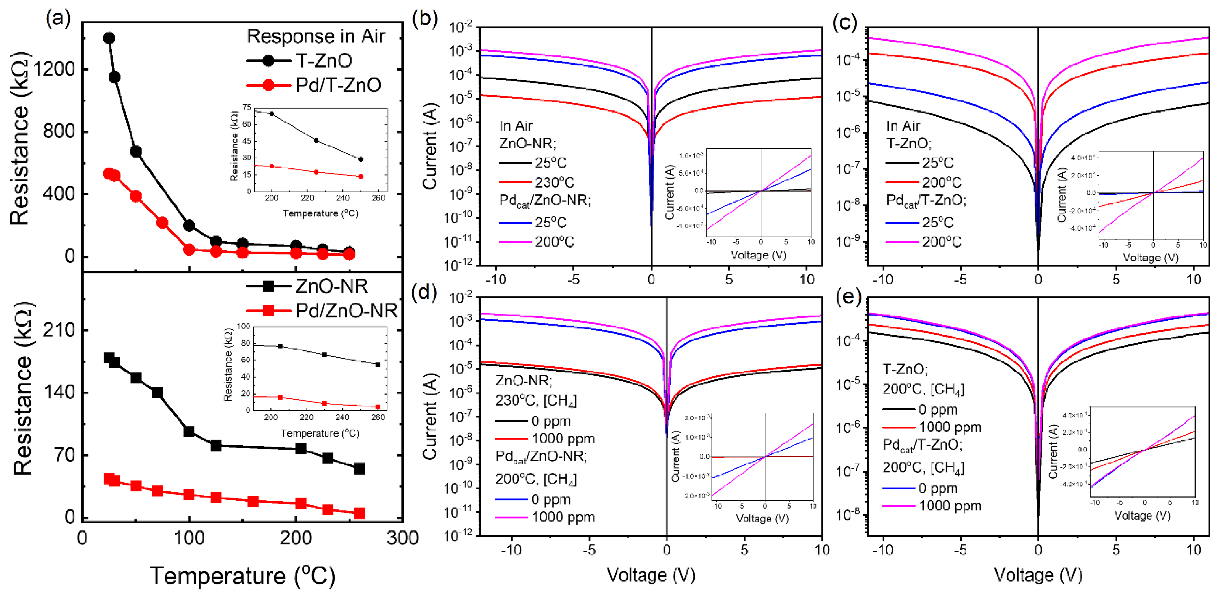
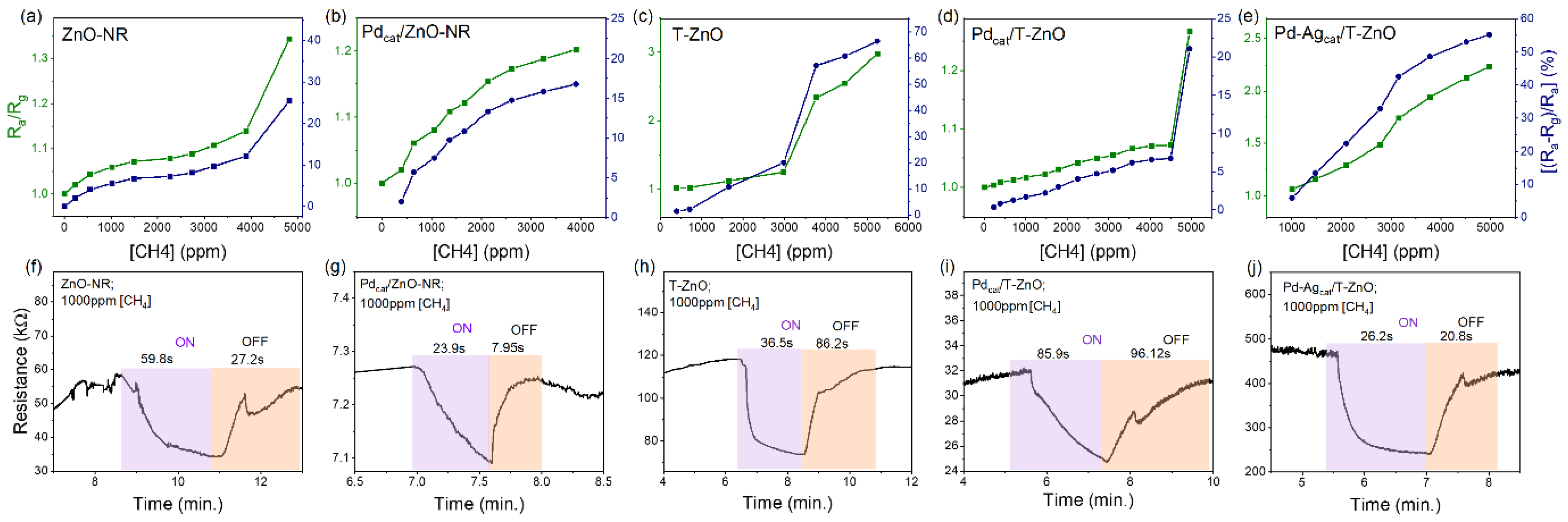
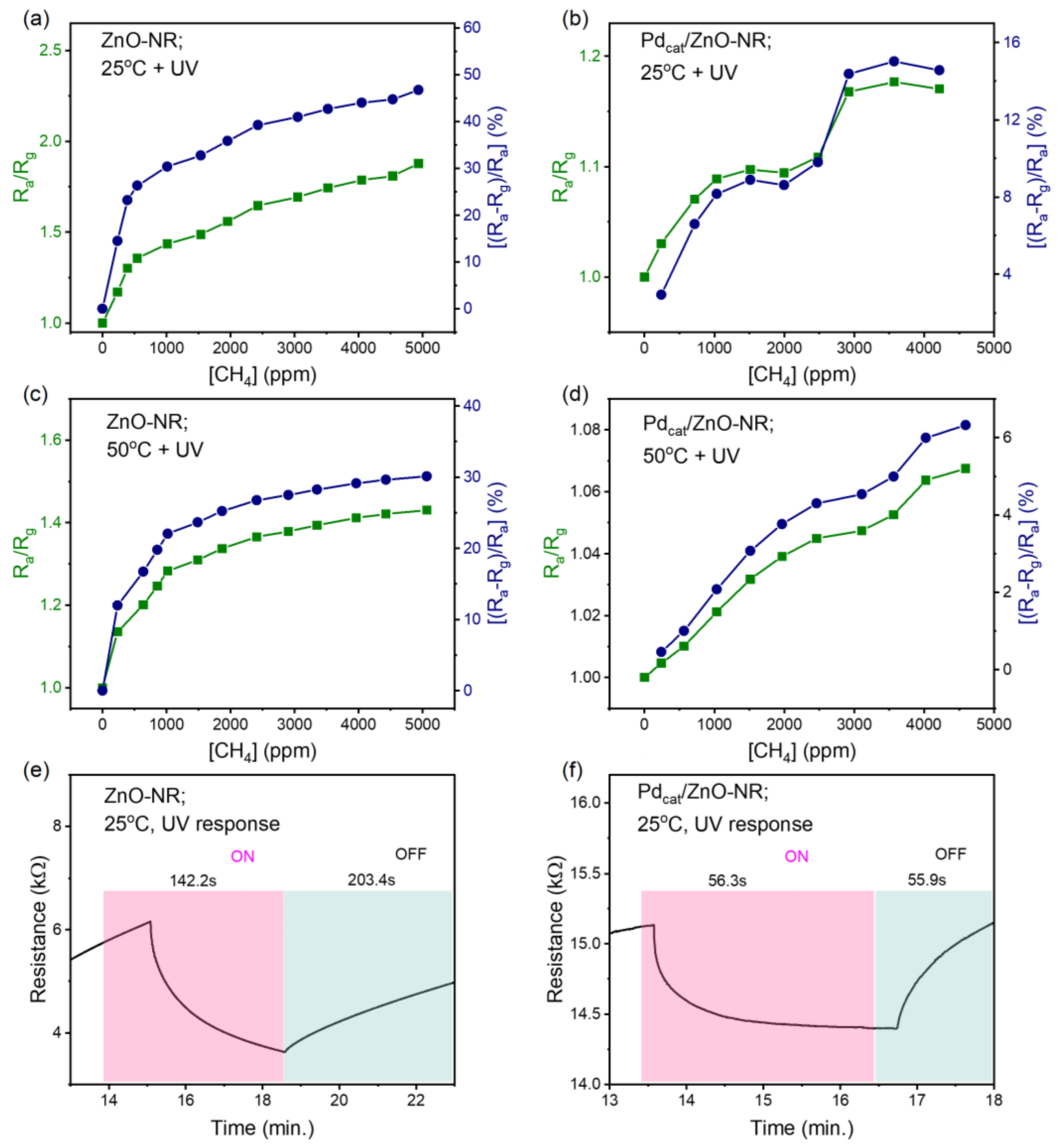
3.2. Methane Gas Sensing Performance of ZnO-NR and Pd-Functionalized Sensors

The methane response of the ZnO-NR thin films was measured in a custom-built chamber system (Scheme 1, panel b). Response magnitude and response percentage were determined from resistance measurements conducted with varying methane concentration at a given or optimal working temperature, defined as the temperature at which the measured conductivity increase was maximal. In Figure 6a,b, the ZnO-NR and Pdcat/ZnO-NR films’ response magnitude and response percentage were determined at 230 °C and 200 °C, respectively.
It was observed that the ZnO-NR response saturated at a lower methane concentration than the Pdcat/ZnO-NR film. It was also observed that the ZnO-NR films had a higher response (~55% at 5000 ppm CH4), compared to the Pdcat/ZnO-NR films (~20% at 5000 ppm CH4). Dynamic on/off cycles of methane were also recorded at temperatures ≥200 °C as in Figure 6f,g and at temperatures between 70 and 100 °C (see Figure S4, Supplementary Materials) which demonstrated the need for a higher temperature operation for a significantly enhanced methane sensing response. The response and recovery times were defined as the time required for the resistance to increase from 10% to 90% of its final value. At lower temperatures, the ZnO-NR and Pdcat/ZnO-NR films had comparable response times of 30.4 s and 33.9 s, respectively. However, the recovery time for the ZnO-NR film was determined to be approximately 65 s, and 139 s for the Pdcat/ZnO-NR film. At the lower temperature, the signal-to-noise ratio was weak which challenged the determination of response and recovery times. At elevated temperatures, the ZnO-NR and Pdcat/ZnO-NR films had response times of 41.7 s and 23.9 s and recovery times of 151 s and 7.95 s, respectively. At both higher and lower temperatures, the Pdcat/ZnO-NR film had a significantly faster recovery time compared to its ZnO-NR counterpart. The films were exposed to increasing CH4 concentration under UV illumination at ambient (25 °C) and at 50 °C (Figure 7a–d). Baseline measurements recorded for ambient UV sensing for both films and the Pdcat/ZnO-NR resulted in faster response and recovery times, compared to the ZnO-NR films (Figure 7e,f). The response percentage of the ZnO-NR films under UV illumination at 1000 ppm CH4 at ambient temperature was ~34%, higher than at 200 °C in the dark. At 50 °C under UV illumination, the response of the ZnO-NR films decreased to ~25% at 1000 ppm CH4. The response of the Pdcat/ZnO-NR films at ambient temperature under UV illumination was found to be ~7.5% at 1000 ppm CH4 and at 50 °C the sensitivity decreased further to 2% at 1000 ppm CH4. For the nanorod-like morphologies, it was observed that the resistance response due to thermal generation-recombination and due to photo-generation were competing, which resulted in decreasing response percentage and response magnitude at 50 °C under UV illumination.

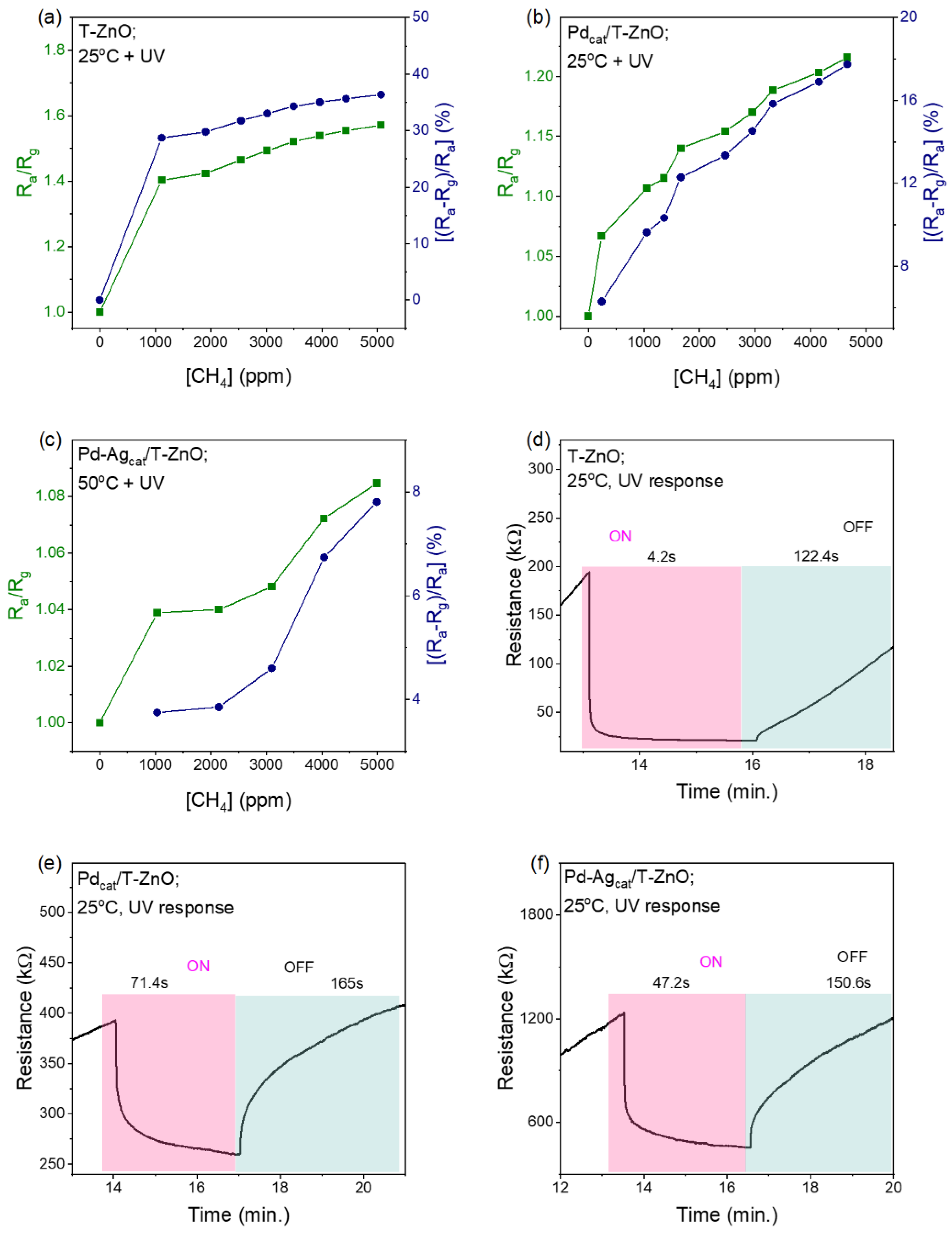
3.3. Performance of T-ZnO and Pd Functionalized Sensors

The response magnitude and response percentile of pristine and modified T-ZnO films are reported in Figure 6c–e. The T-ZnO films both with and without Pd exhibited an improved response to methane sensing at lower temperatures (70 °C) than those from ZnO-NR films. It was found that T-ZnO films had a significantly higher response compared to chemically sensitized Pdcat/T-ZnO at 200 °C. The response percentile of the T-ZnO films was found to be 66%, while it was 22% for the Pdcat/T-ZnO films, 55% for the Pd-Agcat/T-ZnO films, and ~98% for the Pd-dotscat/T-ZnO at 5000 ppm CH4, which is remarkable. The response and recovery times were determined following the same procedure as for the ZnO-NR films at 70 °C and 200 °C. At lower temperatures with 5000 ppm CH4, the T-ZnO had a response time of 72.2 s and a recovery time of 158.8 s, with well-defined changes in the resistance values upon introduction and removal of CH4; the Pdcat/T-ZnO films had a response time of 105 s and recovery time of 34.6 s but with a slightly less-defined change in the signal upon addition or removal of 5000 ppm of CH4; the Pd-Agcat/T-ZnO films on the other hand had a response time of 67.8 s and recovery time of 40.9 s, with well-defined changes in the signal upon addition or removal of 1000 ppm CH4 (see also Figure S4, Supplementary Materials). At a temperature of 200 °C, the ON/OFF response is much better defined. As shown in Figure 6h–j, the T-ZnO films had a response time of 36.5 s and recovery time of 86.2 s, while the Pdcat/T-ZnO had a response time of 85.9 s and recovery time of 96.12 s, the Pd-Agcat/T-ZnO had a response time of 26.2 s and a recovery time of 20.8 s, and the Pd dotcat/T-ZnO had a response time of 19.1 s and a recovery time of 57.2 s. The metal catalysts improved the recovery times consistent with the proposed sensing mechanism including the formation of Pd/Pd-Ag: O2/O complexes which dissociate and react with CH4 to form CO2 and H2O favorably. The T-ZnO films were then evaluated in an ambient environment under UV illumination as in Figure 8a–f, compared to in a gas sensing chamber. As shown in Figure 8a–c, the sensitivity of T-ZnO at ambient temperature with UV illumination decreased to 36%, while the Pdcat/T-ZnO film had a sensitivity of 18% at 5000 ppm CH4. The Pd-Agcat/T-ZnO film exposed to UV illumination at 50 °C had R = 8% at 5000 ppm CH4. The Pd-Agcat/T-ZnO film required additional thermal excitation above room temperature to facilitate CH4 sensing response under UV illumination, but the response magnitude was significantly diminished compared to those at 200 °C. The Pd dotscat/T-ZnO films exhibited response values comparable to or higher than those of the unmodified T-ZnO films at R = 98% at 5000 ppm CH4 which is quite promising. The Pd dotscat/T-ZnO films supported the prospect that there is an upper limit to the concentration of the Pd catalyst loading, above which the response degrades unfavorably. This can be due to the loss of available reaction sites on the exposed facets of the T-ZnO film when Pd loading exceeds an upper bound for surface catalytic reaction to occur. For Pd dotscat/T-ZnO sensors, we observed lift-off of the Pd dots array distributed over a rougher T-ZnO surface after testing cycles, which was challenging since Pd dots functioned as both a surface catalyst in a small area of the film and as an electrode forming nano Schottky barriers. Although the response of the T-ZnO films was lower under UV illumination than at higher temperatures, the T-ZnO films were able to sense varied concentrations of methane at room temperature, which could not be achieved in the dark (OFF) environment at the same temperature. Response of the T-ZnO films under UV illumination at elevated temperatures was investigated, however, like the ZnO-NR films, the resistance measured was not stable. It was postulated that the chemisorption process under thermal and UV activation are unfavorably competing and occasionally nullifying each other, thereby causing the fluctuations in resistance values observed.
Since the signal-to-noise ratio was several times greater, we calculated the limit of detection (LOD) for each film according to IUPAC (International Union of Pure Applied Chemistry) notation. The theoretical LOD can be calculated from the slope of the linear region of the response curve and root-mean-square (rms) deviation at the baseline, i.e., LOD (ppm) = 3 × rmsnoise/slope, where rmsnoise is the standard deviation of noise the number of data points from response curve. The calculated LOD for CH4 for all the sensors studied ranged between 80 ppm and 200 ppm. It was observed that the sensors operating at low temperatures (150–200 °C) showed higher sensitivity compared to the reported room temperature CH4 sensors, or comparable but working at elevated temperatures ≥270 °C [46]. Specifically, for thermal excitation, the LOD ranged from 210 to 152 ppm from unsensitized to sensitized ZnO-NR and from 110 to 30 ppm for T-ZnO sensors, while for UV excitation at room temperature, it ranged from 270 to 138 ppm and from 72 to 23 ppm for UV combined with low-temperature excitation. In addition, the sensors showed promising response/recovery kinetics, which is critical in evaluating the reliability and sustainability of a gas sensor. Table 1 summarizes the methane sensing performance of both ZnO-NR and T-ZnO morphologies and for all the testing environments mentioned above.

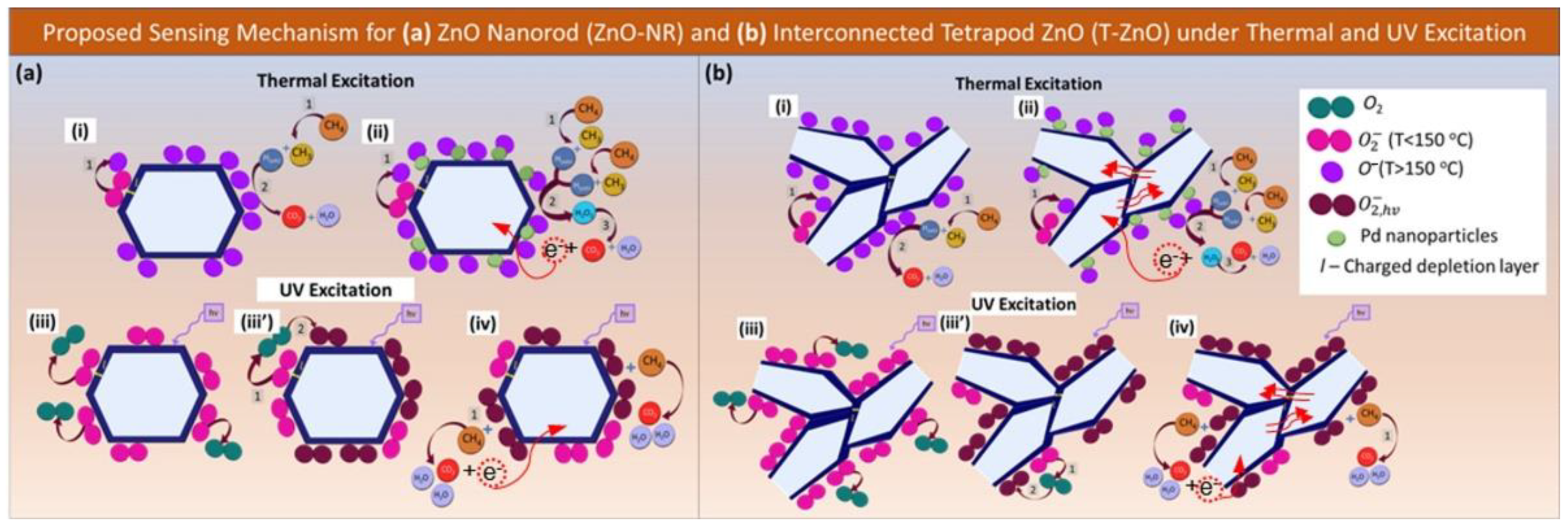
3.4. Proposed Sensing Mechanism and Chemical Pathways

This section expands on the discussion of mechanistic aspects of methane sensing and chemical pathways from ZnO-NR and T-ZnO-based assemblies. It is widely known, that ZnO is an n-type semiconductor due to inherent oxygen vacancies (i.e., VO, VO2+) formed during synthesis and processing and zinc interstitial (i.e., Zni2+, Zni+, Zni) defects due to an excess of zinc in the lattice during deposition [47,48,49,50,51,52]. The oxygen vacancies in ZnO are thermodynamically favorable above absolute zero, but the surface concentration of defects is expected to deviate from bulk concentration driving the gas sensing by modulating the depletion layer commonly described by the energy level band diagram that leads to the upward band bending near the surface for both the valance and conduction bands and space charge layer model [11,43,53,54]. The schematics of a generalized model in terms of space charge layer model including molecular interactions and surface reactions/chemical pathways occurring on exposure to the target gas for pristine and modified ZnO-NR and T-ZnO surfaces provided in Figure 9a,b, respectively. Briefly, at lower temperatures (<100 °C), ZnO has chemisorbed oxygen ions (O2), which are thermally stable and are not easily removed from the surface due to the large adsorption energy of ZnO at room temperature [20].
The formation of the oxygen ions is expressed as follows:
O 2 g a s + e O 2 a d s
The reaction of the molecular oxygen ions (O2) ions with CH4 is energetically unfavorable, especially at room temperature, depicted in Figure S5a,c [Supplementary Materials] for ZnO-NR and T-ZnO films and can be expressed by:
C H 4 a d s + 2 O 2 a d s C O 2 g a s + 2 H 2 O g a s + 2 e
However, at elevated temperatures (>150 °C) in the dark, the surface oxygen ions (O2) further ionizes to form atomic oxygen ions (O) [55,56,57]. Both O2 and O ions are adsorbed on the surface of ZnO to form strongly bonded ZnO: O2/O species [50]. The O2 and O ions react with CH4 to form CO2, and H2O [58]. The proposed chemical pathway that occurs at high operating temperatures (>150 °C) with the O ions is described by Equations (11) and (12) and Figure 9a (i–ii) for ZnO-NR and T-ZnO films, respectively.
O 2 ( a d s ) + e 2 O a d s
C H 4 a d s + 4 O a d s C O 2 g a s + 2 H 2 O g a s + 4 e
Metallic Pd and Ag nanoparticles promote the dissociation of oxygen on the ZnO surface to create more O2/O ions, which also results in the formation of Pd or Pd-Ag: O2/O bonded species [50,51].
Since the bond formed between the oxygen ions and the metallic catalysts is weaker than to the ZnO surface, the oxygen ion is more easily released from the metallic catalysts at lower temperatures, creating more active sites for CH4 molecules to react, in turn lowering the operating temperature [51]. At lower temperatures (<100 °C), the reaction can be expressed by Equation (13) and Figure S5b (see Supplementary Materials) and at higher temperatures by Equations (14) and (15), illustrated in Figure 9a; (ii) for Pdcat/ZnO-NR and Figure 9b; (ii) for Pdcat Pdcat/T-ZnO films. Additionally, Figure 9b shows a higher number of surface reaction sites available in the T-ZnO films due to its networked connectivity and high porosity.
C H 4 a d s + 2 O 2 a d s P d C O 2 g a s + 2 H 2 O g a s + 2 e
C H 4 a d s P d C H 3 a d s + H a d s
C H 3 a d s + 4 H a d s + 4 O a d s C O 2 g a s + 2 H 2 O g a s + 4 e
Under UV illumination close to ZnO bandgap energy, photoinduced holes in the valence band migrate to react with the adsorbed oxygen ions (O2) to form O2(gas), resulting in the desorption of oxygen from the ZnO surface, while additional photoinduced oxygen ions [O2(hν)] are created due to ambient oxygen molecules reacting with photogenerated electrons [49,59]. Photogeneration of electrons is a process whereby an excess of carriers is always created in ZnO [60]. Photoinduced oxygen ions are weakly bonded to the ZnO surface and are easily removed upon the removal of UV light, which can improve recovery times as observed in this work, especially for T-ZnO sensors. The sensing mechanism can be described with a series of Equations (16)–(19) and is depicted in Figure 9a (iii–iv) for ZnO-NR films and Figure 9b (iii–iv) for T-ZnO films, including the formation of O2 from the photogenerated holes combining with the O2 ions and the formation of the photoinduced O2(hν) ions, occurring simultaneously, followed by the photoinduced O2 ions reacting with CH4.
h ν h + + e
h + + O 2 a d s O 2 g a s
C H 4 + 2 O 2 h υ C O 2 g a s + 2 H 2 O g a s + 2 e
At room temperature (or UV combined with low-temperature excitation), the photoinduced oxygen ions react with CH4, and the associated release of electrons leads to a change in the resistance. Thus, while recombination occurs as the oxygen molecules react with the photoelectrons, the resistance measured across ZnO is still lower than the resistance measured in the dark [49]. This allows for the room temperature sensing operation to occur as the CH4 molecules react with the photogenerated oxygen ions. Overall, at elevated temperatures or under UV illumination, once the excitation energy exceeds the bandgap energy, electron-hole pairs are formed [61]. The thermal generation and recombination of carriers (>100 °C) is a dynamic process that attempts to equilibrate the carrier concentration within the ZnO.

4. Conclusions

In summary, we report the development of methane gas sensing platforms based on ZnO-NR arrays and networked T-ZnO films as active layers with a surface decoration of Pd (and Pd-Ag) catalytic nanoparticles excited both thermally and optically with UV illumination close to the bandgap energy. A detailed and systematic study demonstrated that the T-ZnO films were advantageous methane sensors due to their higher porosity, interconnected network morphology, and increased surface-to-volume ratio thereby reducing the barrier height, compared to the ZnO-NR films. It was also found that there is an upper threshold to the catalytic nanoparticle loading, above which the sensor performance decreases which was corroborated using Pd-Ag alloy catalytic dot arrays. Comparable results were found for Pd dot arrays. The primary advantage of utilizing UV illumination as a photocatalyst was that the ZnO-based sensors operated at low (50 °C) or ambient temperatures suitable for detecting methane and other gases in various industrial (factories and manufacturing facilities, mining), environmental (primary and secondary pollutants), and domestic (smoke detectors) applications. We proposed a sensing mechanism based on the space charge layer and surface redox reactions corresponding to chemical pathways.

Supplementary Materials

Supplementary Materials are available free of charge at https://www.mdpi.com/article/10.3390/chemosensors11090506/s1, Lattice parameter calculations from XRD, Tauc plots from optical absorption spectroscopy, temperature-dependent electrical conductivity, dynamic response curves, and sensing mechanism at low temperature.

Author Contributions

Conceptualization, S.G.; methodology, S.G.; software, S.G. and A.K.; validation, S.G., A.K. and B.P.; formal analysis, S.G. and A.K.; investigation, S.G. and A.K.; resources, S.G.; A.K.; and B.P.; data curation, S.G. and A.K.; writing—original draft preparation, S.G. and A.K.; writing—review and editing, S.G., A.K. and B.P.; visualization, S.G. and A.K.; supervision, S.G.; project administration, S.G. and A.K.; funding acquisition, S.G. and B.P. The manuscript was written through the contributions of all authors. All authors have read and agreed to the published version of the manuscript.

Funding

The authors (A.K. and S.G.) acknowledge the funding support by the U.S. Department of Agriculture-National Institute of Food and Agriculture (USDA-NIFA), under Award No. 2019-67021-28991.

Institutional Review Board Statement

Not applicable.

Informed Consent Statement

Not applicable.

Data Availability Statement

Data is contained within the article or Supplementary Materials.

Acknowledgments

The authors acknowledge the resources utilized from the Materials Characterization Lab (MCL) at Penn State University and the assistance from their staff members.

Conflicts of Interest

The authors declare no conflict of interest.

References

  1. Baceninaite, D.; Dzermeikaite, K.; Antanaitis, R. Global Warming and Dairy Cattle: How to Control and Reduce Methane Emission. Animals 2022, 12, 2687. [Google Scholar] [CrossRef] [PubMed]
  2. Neethirajan, S. Transforming the Adaptation Physiology of Farm Animals through Sensors. Animals 2020, 10, 1512. [Google Scholar] [CrossRef]
  3. U.S Environmental Protection Agency. Overview of Greenhouse Gases. 2022. Available online: Epa.gov/ghgemissions/overview-greenhouse-gases (accessed on 1 January 2020).
  4. Santhanam, K.; Ahamed, N. Greenhouse Gas Sensors Fabricated with New Materials for Climatic Usage: A Review. ChemEngineering 2018, 2, 38. [Google Scholar] [CrossRef]
  5. Rojas-Downing, M.M.; Nejadhashemi, A.P.; Harrigan, T.; Woznicki, S.A. Climate change and livestock: Impacts, adaptation, and mitigation. Clim. Risk Manag. 2017, 16, 145–163. [Google Scholar] [CrossRef]
  6. Rezaeipour, A.; Dehghani, S.; Hoghoghifard, S. VOC Sensors Based on Nanoparticles and Nanorods of Nickel Ferrite. IEEE Sens. J. 2022, 22, 16464–16471. [Google Scholar] [CrossRef]
  7. Nikolic, M.V.; Milovanovic, V.; Vasiljevic, Z.Z.; Stamenkovic, Z. Semiconductor Gas Sensors: Materials, Technology, Design, and Application. Sensors 2020, 20, 6694. [Google Scholar] [CrossRef] [PubMed]
  8. Bulemo, P.M.; Cheong, J.Y. Review on Porosity Control in Nanostructured Semiconducting Metal Oxides and Its Influence on Chemiresistive Gas Sensing. ACS Appl. Nano Mater. 2023, 6, 1027–1049. [Google Scholar] [CrossRef]
  9. Bhati, V.S.; Hojamberdiev, M.; Kumar, M. Enhanced sensing performance of ZnO nanostructures-based gas sensors: A review. Energy Rep. 2020, 6, 46–62. [Google Scholar] [CrossRef]
  10. Yamazoe, N.; Fuchigami, J.; Kishikawa, M.; Seiyama, T. Interactions of Tin Oxide Surface with O2, H2O, and H2. Surf. Sci. 1979, 86, 335–344. [Google Scholar] [CrossRef]
  11. Gupta, S.; Knoepfel, A.; Zou, H.; Ding, Y. Investigations of methane gas sensor based on biasing operation of n-ZnO nanorods/p-Si assembled diode and Pd functionalized Schottky junctions. Sens. Actuators B. Chem. 2023, 392, 134030:1–134030:18. [Google Scholar] [CrossRef]
  12. Mondal, B.; Dutta, L.; Roychaudhury, C.; Mohanta, D.; Mukherjee, N.; Saha, H. Effect of Annealing Temperature on the Morphology and Sensitivity of the Zinc Oxide Nanorods-Based Methane Sensor. Acta Metall. Sin. 2014, 27, 593–600. [Google Scholar] [CrossRef]
  13. Yamazoe, N. New approaches for improving semiconductor gas sensors. Sens. Actuators B 1991, 5, 7–19. [Google Scholar] [CrossRef]
  14. Feng, Z.; Gao, C.; Ma, X.; Zhan, J. Well-dispersed Pd nanoparticles on porous ZnO nanoplates via surface ion exchange for chlorobenzene-selective sensor. RSC Adv. 2019, 9, 42351–42359. [Google Scholar] [CrossRef]
  15. Young, S.-J.; Liu, Y.-H. Pd Nanoparticle Adsorption ZnO Nanorods for Enhancing Photodetector UV-Sensing Performance. IEEE J. Electron Devices Soc. 2021, 9, 265–270. [Google Scholar] [CrossRef]
  16. Vayssieres, L. Growth of arrayed nanorods and nanowires of ZnO from aqueous solutions. Adv. Mater. 2003, 15, 464–466. [Google Scholar] [CrossRef]
  17. Wang, Z.L.; Zou, H.; Wang, L. Nanowires and Nanotubes. In Encyclopedia of Applied Physics; Wiley-VCH GmbH: Weinheim, Germany, 2022. [Google Scholar] [CrossRef]
  18. Song, Y.G.; Kim, G.S.; Ju, B.-K.; Kang, C.-Y. Design of Semiconducting Gas Sensors for Room-Temperature Operation. J. Sens. Sci. Technol. 2020, 29, 1–6. [Google Scholar] [CrossRef]
  19. Wang, Z.; Zhu, L.; Sun, S.; Wang, J.; Yan, W. One-Dimensional Nanomaterials in Resistive Gas Sensor: From Material Design to Application. Chemosensors 2021, 9, 198. [Google Scholar] [CrossRef]
  20. Fan, S.-W.; Srivastava, A.K.; Dravid, V.P. UV-activated room-temperature gas sensing mechanism of polycrystalline ZnO. Appl. Phys. Lett. 2009, 95, 142106. [Google Scholar] [CrossRef]
  21. Su, X.; Duan, G.; Xu, Z.; Zhou, F.; Cai, W. Structure, and thickness-dependent gas sensing responses to NO2 under UV irradiation for the multilayered ZnO micro/nanostructured porous, thin films. J. Colloid Interface Sci. 2017, 503, 150–158. [Google Scholar] [CrossRef]
  22. Kumar, R.; Liu, X.; Zhang, J.; Kumar, M. Room-Temperature Gas Sensors under Photoactivation: From Metal Oxides to 2D Materials. Nano Micro. Lett. 2020, 12, 164–167. [Google Scholar] [CrossRef] [PubMed]
  23. Mishra, Y.K.; Modi, G.; Cretu, V.; Postica, V.; Lupan, O.; Reimer, T.; Paulowicz, I.; Hrkac, V.; Benecke, W.; Kienle, L.; et al. Direct Growth of Freestanding ZnO Tetrapod Networks for Multifunctional Applications in Photocatalysis, UV Photodetection, and Gas Sensing. ACS Appl. Mater. Interfaces 2015, 7, 14303–14316. [Google Scholar] [CrossRef] [PubMed]
  24. Mishra, Y.K.; Adelung, R. ZnO tetrapod materials for functional applications. Mater. Today 2018, 21, 631–651. [Google Scholar] [CrossRef]
  25. Knoepfel, A.; Liu, N.; Hou, Y.; Sujani, S.; dos Reis, B.R.; White, R.; Wang, K.; Poudel, B.; Gupta, S.; Priya, S. Development of tetrapod zinc oxide-based UV sensor for precision livestock farming and productivity. Biosensors 2022, 12, 837. [Google Scholar] [CrossRef] [PubMed]
  26. Saboor, F.H.; Ueda, T.; Kamada, K.; Hyodo, T.; Mortazavi, Y.; Khodadadi, A.A.; Shimizu, Y. Enhanced NO2 gas sensing performance of bare and Pd-loaded SnO2 thick film sensors under UV-light irradiation at room temperature. Sens. Actuators Part B 2016, 223, 429–439. [Google Scholar] [CrossRef]
  27. Aghagoli, Z.; Ardyanian, M. Synthesis and study of the structure, magnetic, optical and methane gas sensing properties of cobalt doped zinc oxide microstructures. J. Mater. Sci. Mater. Electron. 2018, 29, 7130–7141. [Google Scholar] [CrossRef]
  28. Wang, J.; Hu, C.; Xia, Y.; Zhang, B. Mesoporous ZnO nanosheets with rich surface oxygen vacancies for UV-activated methane gas sensing at room temperature. Sens. Actuators B Chem. 2021, 333, 129547. [Google Scholar] [CrossRef]
  29. Wyckoff, R.W.G. Crystal Structures, 2nd ed.; Interscience Publishers: Geneva, Switzerland, 1963. [Google Scholar]
  30. Swanson, H.E.; Eleanor, T. Standard X-ray Diffraction Powder Patterns; Commerce, D.O., Ed.; NIST: Gaithersburg, MD, USA, 1953; Volume 1. [Google Scholar]
  31. Kittel, C. Introduction to Solid State Physics; John Wiley & Sons Inc.: Hoboken, NJ, USA, 2005. [Google Scholar]
  32. Cullity, B.D. Elements of X-ray Diffraction, 3rd ed.; Prentice Hall: Hoboken, NJ, USA, 2001. [Google Scholar]
  33. Foo, K.L.; Kashif, M.; Hashim, U.; Liu, W.W. Effect of different solvents on the structural and optical properties of zinc oxide thin films for optoelectronic applications. Ceram. Int. 2014, 40, 753–761. [Google Scholar] [CrossRef]
  34. Yogamalar, R.; Srinivasan, R.; Vinu, A.; Ariga, K.; Bose, A.C. X-ray peak broadening analysis in ZnO nanoparticles. Solid State Commun. 2009, 149, 1919–1923. [Google Scholar] [CrossRef]
  35. Koida, T.; Chichibu, S.; Uedono, A.; Sota, T.; Tsukazaki, A.; Kawasaki, M. Radiative and nonradiative excitonic transitions in nonpolar (1120) and polar (0001) and (0001) ZnO epilayers. Appl. Phys. Lett. 2004, 84, 1079–1081. [Google Scholar] [CrossRef]
  36. Deepak, F.L.; Casillas-Garcia, G.; Esparza, R.; Barron, H.; Jose-Yacaman, M. New insights into the structure of PdAu nanoparticles as revealed by aberration-corrected STEM. J. Crys. Growth 2011, 325, 60–67. [Google Scholar] [CrossRef]
  37. Zhang, B.; Wang, J.; Wei, Q.; Yu, P.; Zhang, S.; Xu, Y.; Dong, Y.; Ni, Y.; Ao, J.; Xia, Y. Visible Light-Induced Room-Temperature Formaldehyde Gas Sensor Based on Porous Three-Dimensional ZnO Nanorod Clusters with Rich Oxygen Vacancies. ACS Omega 2022, 7, 22861–22871. [Google Scholar] [CrossRef] [PubMed]
  38. Edvinsson, T. Optical quantum confinement and photocatalytic properties in two-, one- and zero-dimensional nanostructures. R. Soc. Open Sci. 2018, 5, 180387–180392. [Google Scholar] [CrossRef]
  39. Bedia, A.; Bedia, F.Z.; Aillerie, M.; Maloufi, N.; Benyoucef, B. Morphological and Optical Properties of ZnO Thin Films Prepared by Spray Pyrolysis on Glass Substrates at Various Temperatures for Integration in Solar Cell. Energy Procedia 2015, 74, 529–538. [Google Scholar] [CrossRef]
  40. Saad, R.; Gamal, A.; Zayed, M.; Ahmed, A.M.; Shaban, M.; BinSabt, M.; Rabia, M.; Hamdy, H. Fabrication of ZnO/CNTs for Application in CO2 Sensor at Room Temperature. Nanomaterials 2021, 11, 3087. [Google Scholar] [CrossRef] [PubMed]
  41. Varshni, Y.P. Temperature dependence of the energy gap in semiconductors. Physica 1967, 34, 149–156. [Google Scholar] [CrossRef]
  42. Gür, E.; Tüzemen, S.; Kili, B.; Coşkun, C. High-temperature Schottky diode characteristics of bulk ZnO. J. Phys. Condens. Matter 2007, 19, 196206–196211. [Google Scholar] [CrossRef]
  43. Sze, S.M. Physics of Semiconductor Devices, 2nd ed.; Wiley: New York, NY, USA, 1981. [Google Scholar]
  44. Somvanshi, D.; Jit, S. Mean Barrier Height and Richardson Constant for Pd/ZnO Thin Film-Based Schottky Diodes Grown on n-Si Substrates by Thermal Evaporation Method. IEEE Electron Dev. Lett. 2013, 34, 1238–1240. [Google Scholar] [CrossRef]
  45. Cheung, S.K.; Cheung, N.W. Extraction of Schottky diode parameters from forward current-voltage characteristics. Appl. Phys. Lett. 1986, 49, 85–87. [Google Scholar] [CrossRef]
  46. Liangruska, M.; Laomettachit, T.; Siriwong, C. Enhancing gas sensing properties of novel palladium-decorated zinc oxide surface: A first-principles study. Mater. Res. Express 2021, 8, 45004. [Google Scholar] [CrossRef]
  47. Musa, I.; Qamhieh, N.; Mahmoud, S.T. Synthesis and length dependent photoluminescence property of zinc oxide nanorods. Results Phys. 2017, 7, 3552–3556. [Google Scholar] [CrossRef]
  48. Melnick, D.A. Zinc Oxide Photoconduction, an Oxygen Adsorption Process. J. Chem. Phys. 1957, 26, 1136–1146. [Google Scholar] [CrossRef]
  49. Kumar, M.; Singh Bhati, V.; Ranwa, S.; Singh, J.; Kumar, M. Pd/ZnO nanorods based sensor for highly selective detection of extremely low concentration hydrogen. Sci. Rep. 2017, 7, 236–241. [Google Scholar] [CrossRef]
  50. Chen, R.; Wang, J.; Luo, S.; Xiang, L.; Li, W.; Xie, D. Unraveling photoexcited electron transfer pathway of oxygen vacancy-enriched ZnO/Pd hybrid toward visible light-enhanced methane detection at a relatively low temperature. Appl. Catal. B Environ. 2020, 264, 11855. [Google Scholar] [CrossRef]
  51. Look, D.C.; Hemsky, J.W.; Sizelove, J.R. Residual native shallow donor in ZnO. Phys. Rev. Lett. 1999, 82, 2552–2555. [Google Scholar] [CrossRef]
  52. Janotti, A.; de Walle, C.G.V. Native point defects in ZnO. Phys. Rev. B 2007, 76, 165202. [Google Scholar] [CrossRef]
  53. Xu, L.; Wu, X.C.; Zhu, J.J. Green preparation and catalytic application of Pd nanoparticles. Nanotechnology 2008, 19, 305603–305609. [Google Scholar] [CrossRef] [PubMed]
  54. Karnati, P. Design, Fabrication and Characterization of Core-Shell Nanowires for Resistive Type Gas Sensing; Ohio State University: Columbus, OH, USA, 2021. [Google Scholar]
  55. Wang, Y.; Meng, X.; Yao, M.; Sun, G.; Zhang, Z. Enhanced CH4 sensing properties of Pd modified ZnO nanosheets. Ceram. Int. 2019, 45, 13150–13157. [Google Scholar] [CrossRef]
  56. Ghosh, S.; Roychaudhuri, C.; Bhattacharya, R.; Saha, H.; Mukherjee, N. Palladium-silver-activated ZnO surface: Highly selective methane sensor at reasonably low operating temperature. ACS Appl. Mater. Interfaces 2014, 6, 3879–3887. [Google Scholar] [CrossRef]
  57. Cheng, J.; Hu, D.; Yao, A.; Gao, Y.; Asadi, H. A computational study on the Pd-decorated ZnO nanocluster for H2 gas sensing: A comparison with experimental results. Phys. E 2020, 124, 114237. [Google Scholar] [CrossRef]
  58. Zhang, S.; Li, H.; Zhang, N.; Zhao, X.; Zhang, Z.; Wang, Y. Self-sacrificial templated formation of ZnO with decoration of catalysts for regulating CO and CH4 sensitive detection. Sens. Actuators B Chem. 2021, 330–337, 129286. [Google Scholar] [CrossRef]
  59. Soci, C.; Zhang, A.; Xiang, B.; Dayeh, S.A.; Aplin, D.P.R.; Park, J.; Bao, X.Y.; Lo, Y.H.; Wang, D. ZnO Nanowire UV Photodetectors with High Internal Gain. Nano Lett. 2007, 7, 1003–1009. [Google Scholar] [CrossRef] [PubMed]
  60. Pierret, R.F. Semiconductor Fundamentals; Addison-Wesley: Boston, MA, USA, 1988. [Google Scholar]
  61. Procek, M.; Stolarczyk, A.; Pustelny, T. Impact of Temperature and UV Irradiation on Dynamics of NO2 Sensors Based on ZnO Nanostructures. Nanomaterials 2017, 7, 312. [Google Scholar] [CrossRef]
Scheme 1. (a) ZnO-NR synthesis (b) Custom-built testing system.
Chemosensors 11 00506 sch001
Figure 1. X-ray diffraction of (a) ZnO-NR and Pdcat/ZnO-NR and (b) T-ZnO, Pdcat/T-ZnO, and Pd-Agcat/T-ZnO (JCPDS: 036-1451 for ZnO).
Chemosensors 11 00506 g001
Figure 2. SEM images of ZnO-NR and T-ZnO films (A) undecorated and (B) Pd-functionalized surfaces at different magnifications. The right column (green) shows EDX images revealing elemental mapping and Pd nanoparticles distribution.
Chemosensors 11 00506 g002
Figure 3. Dark field TEM images of ZnO-NR and T-ZnO (a,f) undecorated and (b,g) Pd-functionalized surfaces along with (c) bright field TEM images for Pdcat/ZnO-NR and electron diffraction (insets of (a,f)); (d,e,hj) HAADF-STEM images and EDS mapping of Pdcat/ZnO-NR and Pdcat/T-ZnO revealing Pd nanoparticles distribution for both morphologies.
Chemosensors 11 00506 g003
Figure 4. Optical spectroscopy of ZnO-NR and T-ZnO with and without Pd decoration: (a,c) UV-visible spectra of ZnO-NR, ZnO-NRUV treated, Pdcat/ZnO-NR and T-ZnO, T-ZnOUV treated, Pdcat/T-ZnO; (b,d) photoluminescence (PL) spectra of ZnO-NR, ZnO-NRUV treated, Pdcat/ZnO-NR and T-ZnO, T-ZnOUV treated, Pdcat/T-ZnO.
Chemosensors 11 00506 g004
Figure 5. (a) Resistance response measured in air for ZnO-NR, Pdcat/ZnO-NR, T-ZnO, and Pdcat/T-ZnO, films; (b,c) I–V curves with temperature measured in air; (d,e) I-V curves at ~200 °C in air and 1000 ppm CH4.
Chemosensors 11 00506 g005
Figure 6. (ae) Response magnitude and response percent with CH4 concentration for ZnO-NR at 230 °C, Pdcat/ZnO-NR at 200 °C, T-ZnO at 200 °C, Pdcat/T-ZnO at 230 °C, Pd-Agcat/T-ZnO at 200 °C, Pd-dotscat/T-ZnO at 200 °C; (fj) Dynamic resistance curves showing response/recovery times for 1000 ppm CH4 at 200 °C for ZnO-NR, Pdcat/ZnO-NR, T-ZnO, Pdcat/T-ZnO, Pd-Agcat/T-ZnO, Pd-dotscat/T-ZnO.
Chemosensors 11 00506 g006
Figure 7. Response magnitude and response percent with CH4 concentration under UV excitation at (a,b) 25 °C, (c,d) 50 °C for ZnO-NR and Pdcat/ZnO-NR; (e,f) Dynamic resistance curves showing response/recovery times at 25 °C in air under UV excitation.
Chemosensors 11 00506 g007
Figure 8. (ac) Response magnitude and response percentage with CH4 concentration under UV excitation for T-ZnO at 25 °C, Pdcat/T-ZnO at 25 °C, Pd-Agcat/T-ZnO at 50 °C; (df) Dynamic resistance curves showing response/recovery times at 25 °C under UV excitation for T-ZnO, Pdcat/T-ZnO, Pd-Agcat/T-ZnO.
Chemosensors 11 00506 g008
Figure 9. Proposed mechanistic chemical pathways for (a) ZnO-NR and (b) T-ZnO sensors: (i,ii) Thermal excitation at temperatures > 150 °C for unmodified and Pd-decorated films; (iiiiv) UV excitation at 25 °C for unmodified and Pd-decorated films, note (iii) and (iii’) occur simultaneously.
Chemosensors 11 00506 g009
Table 1. Summary of Methane Sensing Performance of ZnO-NR and T-ZnO Films.
Sample Response *Sensitivity ^ (%)Response Time (s)Recovery Time (s)
ZnO-NR200 °C1.3425.541.7151
90 °C1.022.0830.465
UV at 25 °C1.8846.6--
UV at 50 °C1.4330.18--
Pdcat/ZnO-NR200 °C1.216.723.97.95
70 °C1.000.633.9139
UV at 25 °C1.1714.6--
UV at 50 °C1.076.33--
T-ZnO200 °C2.9866.436.586.2
70 °C1.1210.372.2156.8
UV at 25 °C1.5736.3--
Pdcat/T-ZnO230 °C1.2721.0685.996.1
70 °C1.054.510534.6
UV at 25 °C1.2217.74--
Pd-Agcat/T-ZnO200 °C2.2355.226.220.8
70 °C1.065.2567.840.9
** UV at 50 °C1.087.8--
Pd dotscat/T-ZnO200 °C50.69819.157.2
* Response (R) is determined from Ra/Rg at 5000 ppm CH4. ^ Sensitivity (S) is determined from [(Ra − Rg)/Ra] × 100 at 5000 ppm CH4. ** Pd-Agcat/T-ZnO did not produced stable response at temperature lower than 50 °C, even with UV catalyst.
Disclaimer/Publisher’s Note: The statements, opinions and data contained in all publications are solely those of the individual author(s) and contributor(s) and not of MDPI and/or the editor(s). MDPI and/or the editor(s) disclaim responsibility for any injury to people or property resulting from any ideas, methods, instructions or products referred to in the content.

