Article

Dynamic Analysis of Extendable Hybrid Voltage Lift DC–DC Converter for DC Microgrid

by
Dhafer Almakhles
1,
Divya Navamani Jayachandran
2,
Lavanya Anbazhagan
2,
Marwa Hannachi
3 and
Jagabar Sathik Mohamed Ali
1,*
1
Renewable Energy Laboratory, School of Electrical Engineering, Prince Sultan University, Riyadh 11586, Saudi Arabia
2
Department of Electrical and Electronics Engineering, SRM Institute of Science and Technology, Kattankulathur Campus, Chennai 603203, India
3
Department of Electric Automatic, University of Gabes PEESE (Processes Energetics, Environments, and Electrical Systems), Gabes 6029, Tunisia
*
Author to whom correspondence should be addressed.
Processes 2022, 10(12), 2652; https://doi.org/10.3390/pr10122652
Submission received: 26 October 2022 / Revised: 20 November 2022 / Accepted: 21 November 2022 / Published: 9 December 2022
(This article belongs to the Section Process Control and Monitoring)

Abstract

:
This paper proposes a novel non-isolated high voltage gain dc–dc converter with a boost2 (B2) technique. The derived single-switch hybrid voltage-lift topology generates a higher voltage conversion ratio with less component counts than traditional voltage-lift converters. Furthermore, to show its superiority, the proposed topology is compared with other recent non-isolated dc–dc converters in terms of the number of power components such as inductors, capacitors, diodes, and switches. Moreover, the voltage stress across the power switch is less than the output voltage, which results in using low-rated components and reducing the converter cost. The steady-state analysis of the proposed topology is carried out with the operating modes in continuous and discontinuous conduction modes. The critical inductance for the proposed converter is derived for design considerations. Compared to the other traditional step-up converters, the stresses across the power diodes are highly reduced. The analysis related to the addition of an expander cell with the topology is performed concerning boundary conditions. An efficiency model with loss calculation is presented. Furthermore, the reliability analysis is performed with the military handbook to determine the failure rate of the converter’s components. Finally, the simulation and 50 W prototype model for experimental validation prove the strength of the proposed topology.

1. Introduction

Nowadays, energy sources such as Photovoltaic (PV) and fuel cells have attracted research attention due to the depletion of fossil fuels. The usage of a grid-connected PV system, standalone residential PV system, electric vehicle, LED lighting systems, etc., are increasing. The main limitation in many renewable energy sources is the low output voltage and, therefore, there is a need for the power converter to increase the gain [1,2]. Due to this low voltage, the high gain dc–dc converter is a primary component in the Microgrid system, depicted in Figure 1. It is mainly required to boost the low PV source and battery voltage (12–48 V) to the required voltage level to invert it into AC and feed it into the grid system [3,4]. In this regard, a highly efficient and reliable power converter is essential to integrate a sustainable source into the electric grid [5]. The several different types of PV panels in series or parallel are not the innovative solution to boost the voltage to the required load level. Hence, a front-end high gain dc–dc converter plays a vital role in reducing the cost incurred in adding more PV panels [6]. The DC microgrid has more advantages, such as enhanced power quality and supply security [7,8]. Additionally, the energy storage system is gaining popularity in DC microgrid systems due to the intermittent nature of sustainable energy sources [9].
For a standalone application, the battery is needed to provide an uninterruptable power supply to the loads in this mode. Due to the variation of the PV source, maximum power point tracking (MPPT) is essential for PV powered applications. For MPPT tracking, a battery backup is needed. From Figure 1, high step-up dc–dc converters are required with a high voltage gain, efficiency, and power density for the distributed power generation system [10]. DC–DC converters are categorized into the transformer and transformer less converters [11]. DC–DC converters with transformers are primarily employed for interfacing the renewable energy sources. By increasing the turns ratio of the transformer, the voltage gain of the converters increases. However, unfortunately, the weight of the converter increases with a decrease in efficiency and the pulsed current produced in the converters with the transformer reduces the lifetime of the PV and occupies more space. The non-isolated converters such as conventional boost dc–dc converters have high current ripples and conduction losses with high conversion ratios [12]. An interleaved structure can reduce the input current ripple and can be employed to increase the power level. The voltage multiplier cells coupled inductor and switched passive components are added to boost the gain in dc–dc converters [13]. However, these methods increase the number of passive components and switches. The most commonly used method in non-isolated converters to boost the gain is the voltage-lift method [14]. In 2018, a non-isolated dc converter was proposed with a voltage-lift technique with a component count of nine [15]. However, the voltage gain is boosted only three for D = 0.5. In [16,17,18,19,20], a high gain topology is derived with very high component counts such as 14 and 18. Various high gain concepts are proposed in the literature [20,21,22,23,24,25,26,27,28,29,30,31]. In these topologies, the voltage gain is expandable by adding more inductors, increasing the converter’s size and complexity. Based on the literature, the main limitations in the existing topologies are pulsed input current, more component count, leakage inductance, more voltage, and current stresses across switches and diodes, voltage spikes, etc. [32,33,34]. More switches and passive components increase the bulkiness of the converter and the complexity [35,36,37,38,39,40,41,42,43,44,45,46,47,48]. All these issues are considered for which a new dc–dc converter without a transformer is proposed by integrating the switched inductor and voltage-lift cell into a common branch to obtain a Hybrid Switched Inductor based Voltage-Lift (HSIVL) converter. The proposed converter has the following advantages and is also listed as shown in Table 1:
  • Single switch converter with reduced complexity for controller design.
  • Less number of passive components, which reduces the volume of the converter.
  • Low voltage stress, which reduces the conduction loss and cost of the converter.
  • Output diode voltage stress is less than the output voltage, which minimizes the cost.
  • Efficiency is higher due to fewer component counts.
The derivation of the proposed topology is discussed in Section 2.1. Section 2.2 presents the operating principle of the derived topology. The steady-state analysis of the proposed converter in both continuous and discontinuous conduction modes are dealt with in Section 3.1 and Section 3.2, respectively. The detailed analysis of the converter with a critical inductance analysis is depicted in Section 4. The power loss analysis of the converter is elaborated in Section 5. The dynamic behavior of the derived topology is analyzed by obtaining a frequency response plot and the inference from the study is presented in Section 6. The reliability study is performed and the failure rate of the component is analyzed in Section 7. Section 8 presents the comparative study of the suggested topology with the similar topology reported in the literature. The simulation and experimental study are performed and the results are discussed in Section 9. Section 10 summarizes the inferences and discusses the future scope. Finally, the paper is concluded with the research findings.

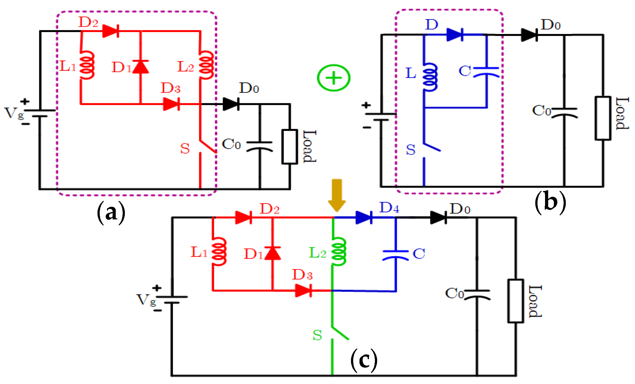
2. Proposed High Voltage DC–DC Converter

2.1. Description of Proposed HSIVL Topology

Figure 1 presents three dc–dc converter topologies. The Switched Inductor (SI) cell in Figure 2a is combined with the Voltage-Lift (VL) cell in Figure 2b to derive a Hybrid Switched Inductor-based Voltage-Lift (HSIVL) converter, which is illustrated in Figure 2c.
The gain of the super-lift boost converter is (1 + D/(1 − D) and the gain of elementary Luo converter is (2 − D/(1 − D). The voltage conversion ratio of both the converters depicted in Figure 2a,b is less than the proposed topology. The switch voltage stress of the super-lift boost converter is equal to the output voltage. The extendable capability is not possible in an elementary Luo converter. The special features of the suggested topology by the integration of the topologies are in Figure 2a,b.
  • The voltage gain is high compared to super-lift boost and elementary Luo converter.
  • The switch voltage stress is not equal to the output voltage, which reduces the Rds (on) and increases the efficiency of the converter.
  • Extension of the voltage gain is feasible without increasing the power switch count.

2.2. Modes and Operating Principle of the HSIVL Topology

2.2.1. Mode I

When the switch is conducting, the diodes D2, D3, and D4 will be forward biased and due to the topology, switched inductors will be connected in parallel. The inductors L1 and L2 will be charged simultaneously along with the capacitor to the full supply voltage. At the same time, diodes D1 and D0 will be reverse biased and C0 will be supplying the load Considering Kirchhoff’s Voltage Law in Figure 3a, the inductor voltage is obtained as:
V L 1 = V L 2 = V C = V g
I C = I g 3

2.2.2. Mode II

When the switch is in the non-conducting state, diodes D1 and D0 will be forward biased and, due to this, the switched inductors will be connected in series. The energy stored in inductors L1 and L2 will be discharged along with the capacitor C to the load and charge capacitor C0. At the same time, diodes D2, D3, and D4 will be reverse biased. Figure 4a,b depict the key waveforms of the HSIVL converter. Similar to the ON condition (Mode I), the inductor voltage is acquired from Figure 3b.
V L 1 = V L 2 = V C = V g V o 3
I C = I L 1 = I L 2 = I g

2.2.3. Mode III

When the switches and diodes are not conducting, it will lead to a discontinuous mode of operation. This mode might occur due to large current ripple at light load conditions.
The capacitor CO alone supplies the load and starts discharging. The voltage gain of the converter in this mode not only depends on the duty cycle, but also becomes load dependent.

3. Steady-State Analysis

3.1. Continuous Conduction Mode

The voltage balance law is applied to Equations (1) and (3) and the following relationship is obtained:
0 D T V g d t + D T T V g V O 3 d t
By simplifying (5), the voltage conversion ratio is determined as:
G V C C M = V O V g = 1 + 2 D 1 D
The general voltage gain expression for the derived topology with N, which is the number of expander cells:
G V C C M = V O V g = 1 + 2 N D 1 D
The ampere second balance law is applied to Equations (2) and (4) and the following relationship is obtained:
I L 1 ( a v g ) = I L 2 ( a v g ) = I O G V C C M 1 + 2 D
The sensitivity of the output voltage with respect to duty cycle is:
S = d V O d D = V g [ 1 D ] 2
The value of sensitivity is just similar to the conventional boost converter. The sensitivity, S, remains the same for N number of expander cells. The output-power capability of the proposed topology is:
C P = P O V S W I S W = 1 D 3 D
If D increases, the output-power capability, Cp starts to decrease.

3.2. Stress across the Semiconductor Devices

From the steady-state analysis, the stresses across all the components of the derived topology with average and Root Mean Square (RMS) currents of the semiconductor devices are obtained and listed below.
The maximum voltage stress across the switch is not equal to the output voltage and it is expressed as:
V S W ( max ) = V O ( 2 G V + 1 ) 3 G V
The RMS current through the switch is determined as:
I S W ( R M S ) = I O G V D
Similarly, the diodes voltage and currents are determined as:
V D 1 ( max ) = V D 2 ( max ) = V D 3 ( max ) = V D 4 ( max ) = V O G V ; V D O ( max ) = 3 V g D 1 D
I D 1 ( R M S ) = I D O ( R M S ) = I O G V 1 D 1 + 2 D
I D 2 ( R M S ) = I D 3 ( R M S ) = I O G V D 1 + 2 D

3.3. Stress across the Passive Components across the Semiconductor Devices

The voltage across the capacitors (C and Co) and current through the inductors (L1 and L2) are acquired and presented for the design of the passive components.
V C ( max ) = V O G V
I L 1 ( R M S ) = I L 2 ( R M S ) = I O G V 1 + 2 D
I C O ( R M S ) = I O G V D 1 + 2 D
Switchs (9)–(16) are used to find the ratings of semiconductor devices and passive components.
The design guidelines for the components are presented in the later section.
The switch and output diode voltage stress depend on three parameters: input voltage, duty cycle, and the number of expander cells, N. To find the greater influencing factor on the switch, a graph is plotted in Figure 5. It is observed from the figure that the switch voltage stress is directly proportional to the input voltage and expander cell and both these factors are great at influencing compared to the duty cycle. The output diode, Do, has the similar voltage stress as the switch and it is equal to VO − Vg. Hence, this analysis will help in the selection of the number of expander cells and input voltage. To find the impact of expander cells on the voltage stress on the component, the stress on the switch and diodes are tabulated for various numbers of expander cells (1, 2, …, N) and presented in Table 2.
Figure 2c depicts the operating mode of HSIVL converter in DCM. Using Figure 2d, the average value of inductor (L1) current in DCM is obtained by the Volt-second balance principle.
V L 1 ( t ) = D 1 V g + D 2 ( V g V O 3 ) + D 3 ( 0 ) = 0
Simplifying (19), the output voltage in DCM condition is determined as:
V O = [ 1 + 3 D 1 D 2 ] V g
The diode (D1) current is identical to the inductor (L1) current during the non-conducting state of switch S. The dc component of diode (D1) current is:
i D 1 ( t ) = 1 T S 0 T S i L 1 P e a k D 2 T S d t
It is observed that in the second interval, the dc component of the inductor (L1) current is equal to the dc component of the diode (D1) current. Therefore:
V O R O ( 1 D 1 ) = V g D 1 D 2 T S 2 L 1
To eliminate D2, (22) is simplified to be:
D 2 = 3 D 1 V g V O V g
Using Equation (23) in (20), the following quadratic expression is obtained.
V O 2 V g V O 3 V g 2 D 1 2 ( 1 D 1 ) K L 1 = 0
Solving the above equation, the voltage conversion ratio of the HSIVL converter in DCM is acquired as:
V O V g = G V D C M ( D 1 ,   K L 1 ) = 1 ± 1 + 12 D 1 2 ( 1 D 1 ) K L 1 2
where K L 1 = 2 L 1 R O T S .
Equation (25) presents the voltage conversion ratio of the HSIVL converter in DCM. To analyze the voltage, gain in DCM, a plot is drawn for various values of KL1. It is noted from Figure 6 that the voltage gain decreases with the increase in the value of KL1.

4. Discussion

The design of inductors and capacitors are critical in predicting the performance of the converter, voltage, and current ripples, compactness, losses, filter size, and efficiency. The topology proposed is designed for a normal condition as well as for a worst condition case where the converter can be operated without crossing the limitations. The inductor value is selected based on the desired current ripple and the capacitor values are based on the desired voltage ripple. The average inductor current is larger than the ripples in the inductor (L1) current and then the converter operates in CCM.
I L 1 > Δ i L
By substituting the value of the average inductor current and the ripple current in Equation (26), it provides:
V 0 R 0 ( 1 D ) > V O ( 1 D ) D 2 ( 1 + 2 D ) f s L 1
Solving the above expression to derive the value of inductor will provide:
2 L 1 f s R o > D G V 2
L 1 , L 2 > R 0 ( 1 D ) 2 D 2 ( 1 + 2 D ) f s
where K cric ( L 1 ) ( D ) = D ( 1 D ) G V
K L 1 > K c r i c ( L 1 ) ( D )   CCM
Kcric(L1) depends on duty cycle and decides the transition from CCM to DCM mode. Figure 7 illustrates the operation of HSIVL converter concerning critical inductance, which is the boundary between the continuous and discontinuous region. KL1 is used to verify the operation of the converter in continuous or discontinuous modes.
The output current at the boundary condition of CCM and DCM is provided as:
I O B = V O D ( 1 D ) 2 2 f s L ( 1 + 2 D ) 2
Figure 7b presents the normalized load current at the boundary between CCM and DCM for N = 1, 2, and 3. From this graph, it is observed that the CCM region can be extended with the increase in the number of expander cell, N.

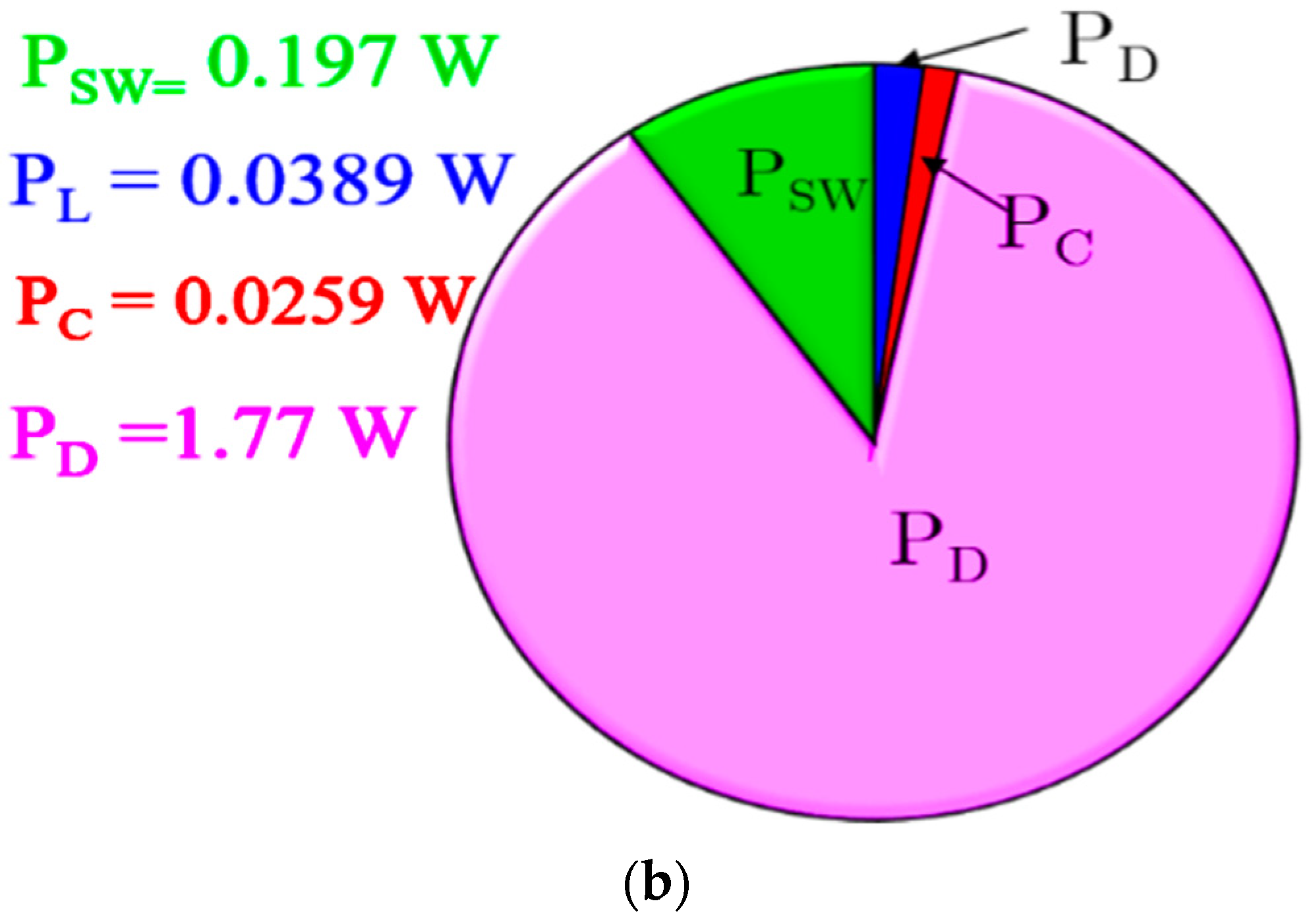
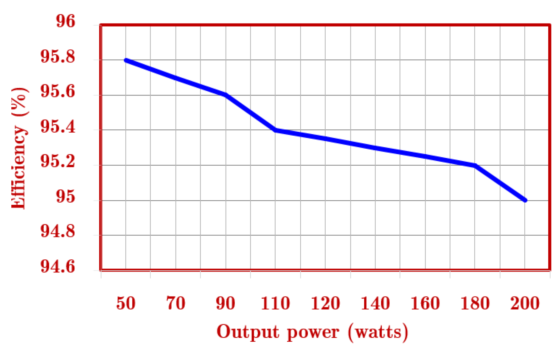
5. Efficiency Analysis

For efficiency analysis, the ripples of inductors and capacitors are neglected for the HSIVL converter. All through this derivation, the MOSFET drain-source resistance is taken as RS, the forward voltage and forward resistance of the diodes are considered as RD and VD, respectively. The DC resistances of the inductors are taken as RL. Similarly, the Equivalent Series Resistance (ESR) of capacitors C and CO are assumed to be RC and RCO, respectively.
The equivalent circuit for the HSIVL converter is presented in Figure 8a to carry out efficiency analysis.
The parameters chosen to calculate the efficiency of the HSIVL converter are Vg = 12 V, VO = 48 V, fS = 10 kHz, D = 0.5, RO = 50 Ω, RS = 9 mΩ, VD = 0.42 V, RD = 2.1 mΩ, RL = 4.5 mΩ, and RC = RCO = 12 mΩ. Table 3 presents the loss equations of all the components in the converter. Figure 8b summarizes the losses distribution in various components of the proposed HSIVL converter. The conversion efficiency is 95.8% at 50 W.

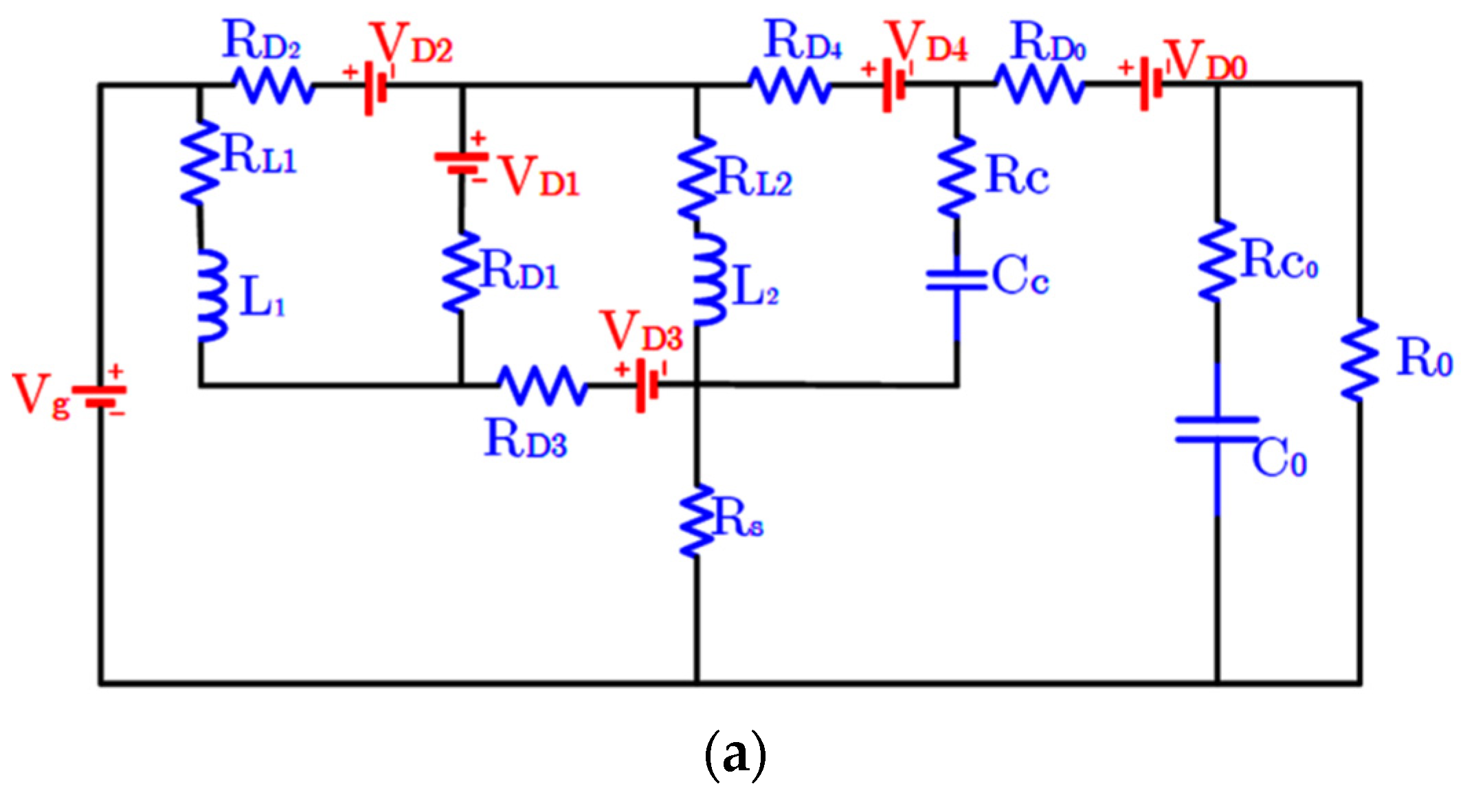
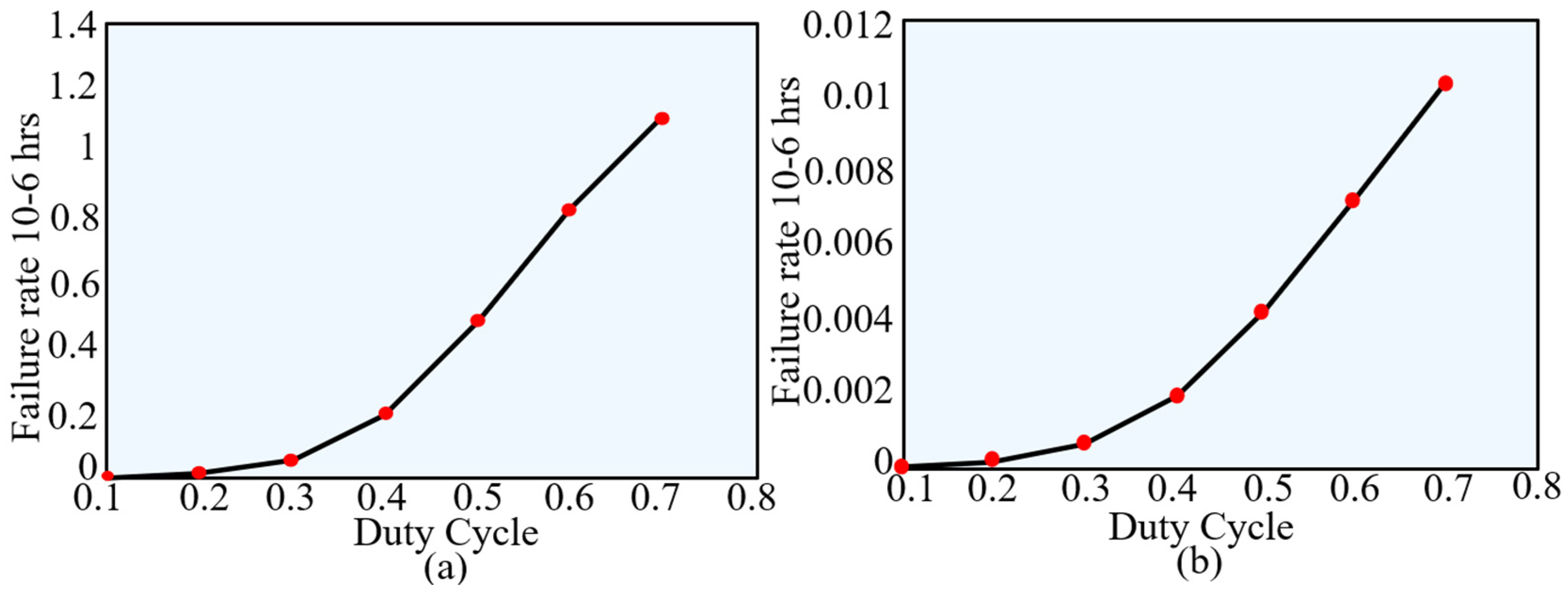
6. Dynamic Analysis of the Converter

In this section, the dynamic characteristics of the proposed topology are studied with the derivation of the input to output and control to output transfer function. The converter is modeled with state-space modeling technique and the following transfer functions are obtained.
In this dynamic analysis, the inductor (L1, L2, and C) are parallelly charged in ON mode and discharged serially in the subsequent mode. Hence, all these passive components are considered as single component, L. The proposed topology is reduced to a two-order system due to this assumption.
The derived input to output transfer function is expressed as:
V O ( s ) ˜ V g ( s ) ˜ = R O ( 1 + 2 D ) ( 1 D ) 3 L C O R O s 2 + 3 L s + ( 1 D ) 2 R O    
The control to output transfer function is obtained as:
V O ( s ) ˜ d ( s ) ˜ = [ ( 1 + 2 D ) ( 1 D ) V g 3 L I O s ] ( R O / ( 1 D ) ) 3 L C O R O s 2 + 3 L s + ( 1 D ) 2 R O  
From (32) and (33), the frequency response plot is acquired using the same specifications used for simulation and experimental study. After substituting the values of the element, the following expressions are obtained:
V O ( s ) ˜ V g ( s ) ˜ = 217.5 2.6 e 6 s 2 + 3 e 4 s + 21.75    
V O ( s ) ˜ d ( s ) ˜ = 2088 0.03966 s 2.6 e 6 s 2 + 3 e 4 s + 21.75  
The frequency response plots of (29) and (30) are obtained and presented in Figure 9a–d. From these figures, it is noted that the derived topology is a non-minimum phase system because the zero lie in the right half of the s-plane. However, in the case of the control to output transfer function, the poles lie in the jɷ axis of the s-plane. Hence, the system may fall under marginally stable. These observations recommend designing a controller for the converter to handle the perturbation in input and output voltage condition. The above section explains the dynamic study of the HSIVL converter. The additional feature of the converter with respect to the dynamic analysis is the derivation of the extendable topology’s transfer function since the topology is considered with equal inductance and also the voltage across the inductors and capacitors are assumed to be equal for the analysis. In this regard, it will be easier in designing the passive components of the converter and also the controller design.

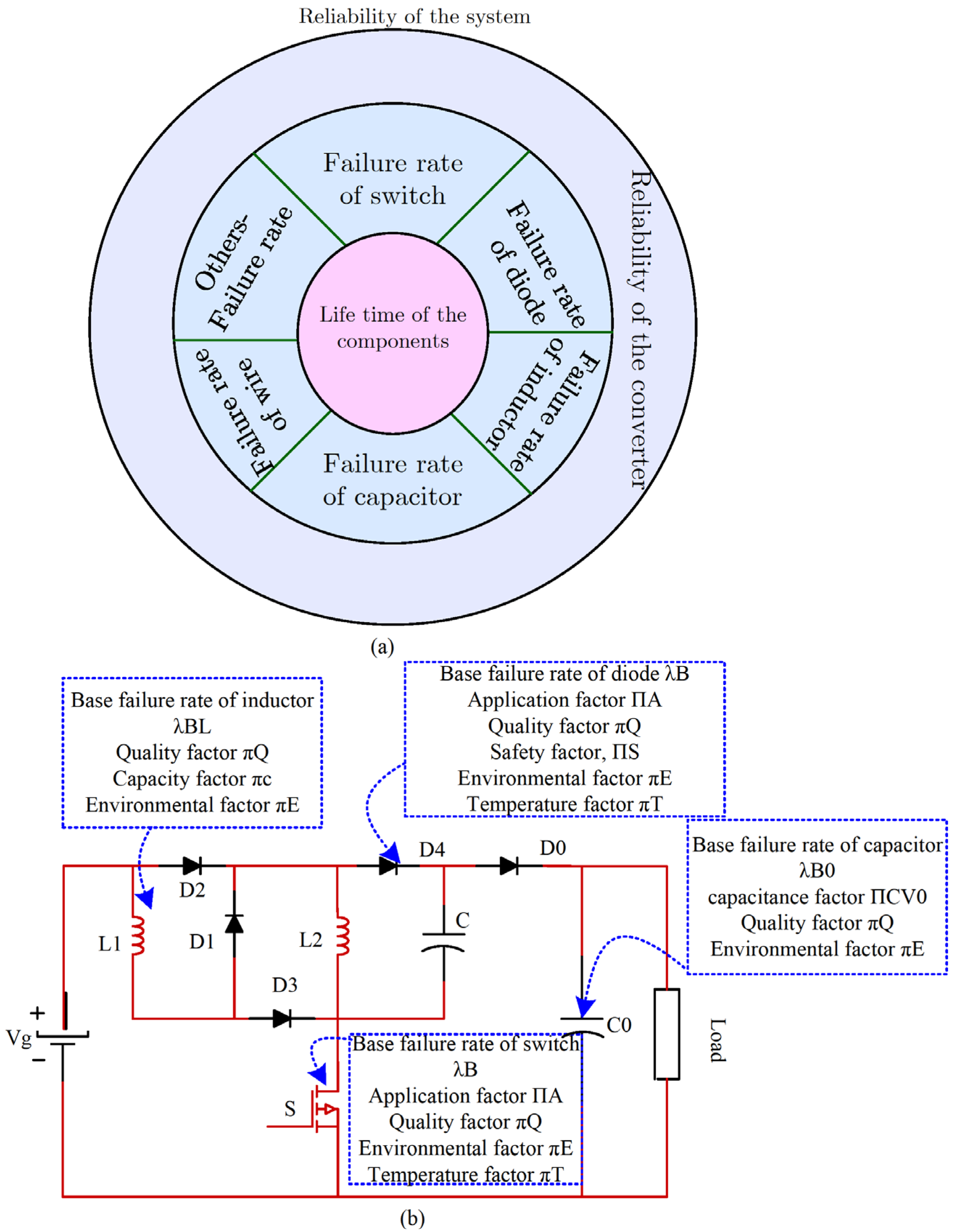
7. Reliability Analysis

7.1. Factors Affecting the Converter’s Lifetime

More than 80% of the system cost is spent on the converter if a failure occurs. Therefore, estimating the reliability of the converter is requisite before the installation of the system. This section introduces the role and impact of various components of the system in the reliability study. This provides a deep insight into the parameters involved in the reliability estimation of the system. The reliability, as mentioned earlier, revolves around the failure rate of the different components in the converter circuit provided in Figure 10a,b. The power semiconductor devices and its failure rate play a vital role and have a greater impact on the system’s entire reliability depending majorly on the converter reliability. This, in turn, depends on the components connected. Therefore, the calculation of the component’s failure rate and the converter’s reliability is the main objective of this section.
The study carried out on the reliability predetermines the lifetime of the system using the equations as presented in (36)–(45).
Switch:
λ S W = λ B π T   π A   π S   π Q   π E  
T j = T c + θ j c P S W
π T   = e 1925 ( 1 T j   + 278 1 298 )
λ S W = 1.38 e 1925 ( 1 318 + 25.7 ( D 2 ( 1 D ) 2 ( 0.093 ( 1 + 2 D ) 4 ( 1 D ) 2 + 1 61.7 ) ) 1 298 )
Diode:
λ D = λ B π T   π A   π S   π Q   π E  
π T   = e 3091 ( 1 T j   + 273 1 298 )
λ D = 0.0147 e 3091 ( 1 98 + P D 1 298 )
P D = 1 + 2 D 1 D ( ( 1 + 2.5 D 1 D ) 11.4 + ( 4 D 1 D ) 1.14 ( 1 + 2 D 1 D ) )
Inductor:
λ L = 0.0014 e ( 298 + 0.08 ( 1 + 2 D ) 2 ( 1 D ) 4 ) 409
Capacitor:
λ C = 0.028 10 6   hours

7.2. Impact of Failure Rate of Switch and Diode

The impact of varying the duty cycle on the failure rate of the switch and diode is shown in the graph below. The optimum selection and operation of the duty cycle are vital in deciding the lifetime of the power semiconductor devices, as shown in Figure 11a,b. The failure rate switch and diode characteristics are plotted for various values of duty cycle.
The analysis shows that the failure rate of the power switch in the converter has the highest rate of failure compared to the other components in the circuit. Therefore, to achieve better reliability, the failure rate of the switch must be reduced. The failure rate of the switch depends on the power loss in the switch, voltage, and current stress across the switch. Selecting the proper rating of the switch can avoid the losses and derating of the converter. This also reduces the failure rate of the switch. Thus, this section provides information about the reliability analysis of the converter and its importance. Further investigation and necessary actions to be performed to improve reliability are the future scopes of this study.

8. Comparative Analysis

The comparative analysis of the key performance metric parameters considered in the proposed converter and the existing converters are listed in Table 4. It is seen that the proposed converter has fewer component counts and switch voltage stress compared to super lift converter [18] and AH-SLC [20]. As the voltage gain increases, the number of inductors required in the proposed converter is half of that required for converters in [10,11] as shown in Figure 12a.
The switch voltage stress in the proposed converter is only 50% of the converter in [19] and 75% as the converter in [20], which is revealed in Figure 10b. Moreover, the proposed topology has a scope for voltage gain expansion, which is not possible in the converter provided in [20]. For voltage gain > 5, the HSIVL converter has a lower increase in the number of inductors compared to the converters [18,19] used for the comparison. The proposed converter is not compared with converter [20] for the number of inductors due to the fixed number of inductors in that converter [20]. Furthermore, the proposed converter is also compared with other performance metrics such as the voltage gain and switch voltage stress. Similarly, the HSIVL converter has lower voltage stress for higher voltage gain compared to other converters in the literature where the voltage stress is equal to the output voltage. Moreover, the firm features of the HSIVL converter are highlighted by further comparing with the converters presented in [21,22,23]. All the topologies considered for comparison have component counts more or less similar to the proposed topology. The gain is observed to be similar to the converters considered [21,22,23] for study.
Several topologies are derived with extendable form either in increasing the turns ratio of the coupled inductor in the converter [35] and adding N number of voltage multiplier cells [36]. In [36], the voltage gain of the converter is (N + 1)D/(1 − D) with the component count of 11, whereas the proposed topology presents the voltage gain of (1 + 2ND)/(1 − D). From this comparison, it is observed for N = 1 and D = 0.5 that the proposed HSIVL topology provides the gain twice that of the converter in [36] with a lower component count.

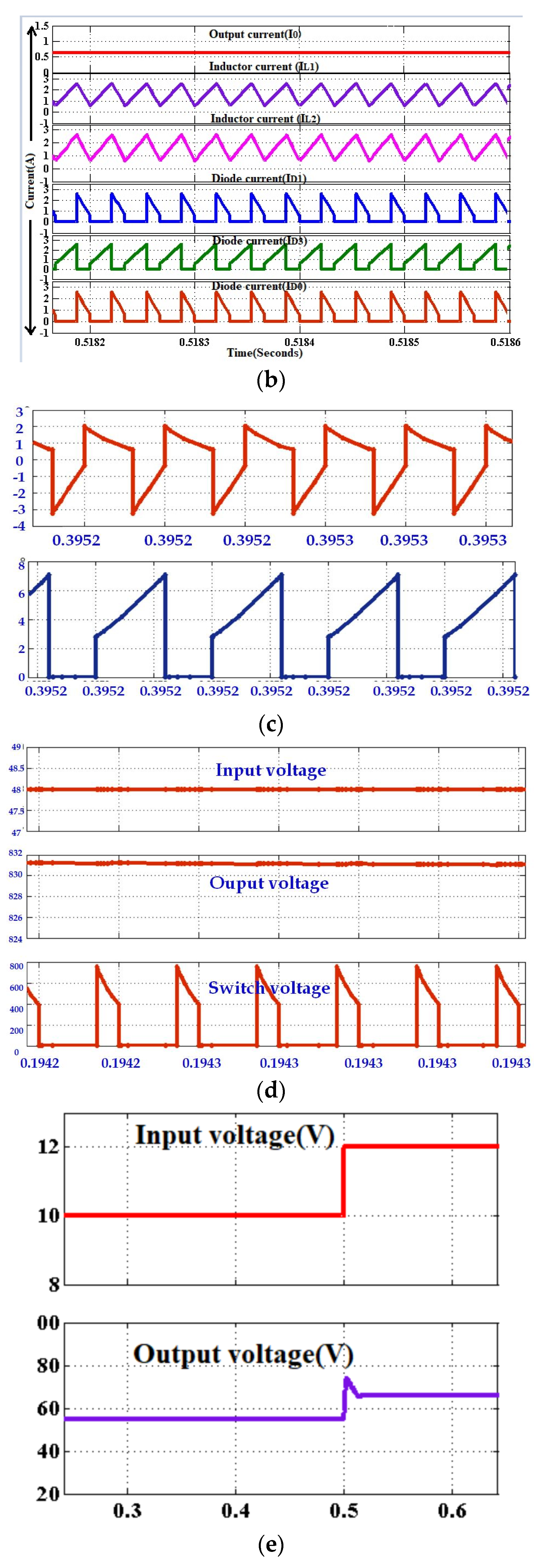
9. Simulation and Experimental Results

This section discusses the simulation results followed by hardware results. The derived topology is simulated in MATLAB-Simulink software and the results are presented in Figure 13a,b. Figure 13a depicts the output voltage, switch voltage, diode voltage, and capacitor voltage waveforms of the HSIVL converter. The current through the components of the converter is illustrated in Figure 13b. The proposed converter specifications for simulation are chosen as: Vg = 12 V, VO = 66 V, D = 0.5, fS = 50 kHz, L1 = L2 = 50 µH, RO = 87 Ω, C = 100 µF, and CO = 100 µF. The illustrated simulated waveform shows an output voltage of 65.5 V for an input voltage of 12 V. Finally, it is validated by testing the prototype in the laboratory. The switch voltage waveform shows that the switch stress is less than the output voltage. The switch and capacitor current with a high value of ESR to reduce the impulse is presented in Figure 13c. The suitability of the converter for higher voltage is depicted in Figure 13d with 48 V input voltage, 832 V output voltage, D = 0.7, and the number of expander cells N = 3. Finally, the transient response of the converter is observed by performing step changes in the input port and the results are depicted in Figure 13e.
A 50 W prototype circuit with the specifications mentioned in Table 5 is implemented to validate the theoretical analysis of the derived converter and it is presented in Figure 14a–h. Figure 14a,b show the input and output voltage for a duty cycle of 0.6. Figure 14c,d depict the gate pulse and switch voltage of the HSIVL converter. It is observed that the maximum switch voltage is (2VO + Vg)/3.
It is also noted that the voltages of diodes (D1–D4) and capacitor (C) are equal to the input voltage. This depicts that the stress on the diodes is much lower and it is independent of the boosted output voltage; these are illustrated in Figure 14e,g. The output diode voltage is presented in Figure 14f, which is equal to the difference of output and input voltage. The inductor voltage is presented in Figure 14h. The photograph of the tested hardware is shown in Figure 14i. Finally, the whole setup implemented for validating the theoretical analysis is presented in Figure 14j.
The maximum voltage across the diodes (D1, D2, and D3) is equal to the supply voltage, Vg, which is illustrated in Figure 14c. The voltage across the output diode is similar to the switch voltage, which is depicted in Figure 9d. It is seen that the inductor currents (IL1, IL2) are continuous, which are presented in Figure 14e. Table 6 validates the HSIVL converter. It is observed from Figure 15 that the efficiency of the converter starts to droop when the output power of the converter increases. Since the component count is less and the switch voltage stress is Vo–Vg, the efficiency of the converter is observed to be theoretically high. Figure 15 provides the efficiency curve for various loads that are calculated theoretically. The efficiency at the rated load is 95.8%, which can be observed from Figure 15. On average, the HSIVL converter shows 95% efficiency for various output powers.

10. Conclusions

A novel hybrid power converter structure with a switched inductor and voltage-lift cell was derived and analyzed. The proposed topology uses lower voltage stress on the switches and diodes, which further minimizes the cost of the converter confirmed by the analysis and experimental results. The voltage stress across the output diode in most of the high gain dc–dc converter is equal to the output voltage. In the derived topology, the stress across the output diode of the derived topology is the difference of output and input voltage, which reduces the cost and increases the reliability of the component. According to the military handbook for reliability prediction, the failure rate of the diode depends on the voltage stress ratio. Hence, the reduction in maximum voltage stress increases the maximum time to failure of the component. The switching and conduction losses are analyzed and it shows that the proposed topology offers low losses due to lower number of power components. The significant factors affecting the lifetime of the converter are identified and analyzed. The reliability study helps us to find the optimum value of the duty cycle with respect to the failure rate of the passive and active components. To demonstrate the theoretical results, a 50 W prototype has been assembled in the laboratory. The experimental results have validated and proved that the proposed converter is suitable for high voltage gain applications such as photovoltaic systems, fuel cell, etc.

Author Contributions

Conceptualization, D.N.J., L.A. and D.A.; methodology, D.N.J. and J.S.M.A.; software, D.N.J. and L.A.; validation, D.N.J. and D.A.; formal analysis, L.A. and J.S.M.A.; investigation, D.N.J. and D.A.; resources, M.H. and D.A.; data curation, M.H.; writing—original draft preparation, D.N.J., D.A. and L.A.; writing—review and editing, M.H. and J.S.M.A.; supervision, D.N.J. and J.S.M.A.; project administration, D.N.J. All authors have read and agreed to the published version of the manuscript.

Funding

This research received no external funding.

Institutional Review Board Statement

Not applicable.

Informed Consent Statement

Not applicable.

Data Availability Statement

All data generated or analyzed during this study are included in this article.

Acknowledgments

The authors would like to acknowledge the support of Prince Sultan University for paying the Article Processing Charges (APC) of this publication.

Conflicts of Interest

The authors declare no conflict of interest.

Nomenclature

MPPTMaximum power point tracking
PVPhotovoltaic
NNumber of expander cells
DDuty cycle
GvVoltage gain
SStress ratio
CCMContinuous Conduction Mode
DCMDiscontinuous Conduction Mode
λSWFailure rate of the switch
λDFailure rate of the diode
λLFailure rate of the inductor
λCFailure rate of the capacitor
πTTemperature factor
πEEnvironmental factor
πSStress factor
πQQuality factor
πAApplication factor

References

  1. Li, W.; He, X. Review of Nonisolated High-Step-Up DC/DC Converters in Photovoltaic Grid-Connected Applications. IEEE Trans. Ind. Electron. 2010, 58, 1239–1250. [Google Scholar] [CrossRef]
  2. Leon-Masich, A.; Valderrama-Blavi, H.; Bosque-Moncusi, J.M.; Martinez-Salamero, L. A High-Voltage SiC-Based Boost PFC for LED Applications. IEEE Trans. Power Electron. 2015, 31, 1633–1642. [Google Scholar] [CrossRef]
  3. Bhaskar, M.S.; Meraj, M.; Iqbal, A.; Padmanaban, S.; Maroti, P.K.; Alammari, R. High Gain Transformer-Less Double-Duty-Triple-Mode DC/DC Converter for DC Microgrid. IEEE Access 2019, 7, 36353–36370. [Google Scholar] [CrossRef]
  4. Lakshmi, M.; Hemamalini, S. Nonisolated High Gain DC–DC Converter for DC Microgrids. IEEE Trans. Ind. Electron. 2017, 65, 1205–1212. [Google Scholar] [CrossRef]
  5. Alghaythi, M.L.; O′Connell, R.M.; Islam, N.E.; Khan, M.M.S.; Guerrero, J.M. A High Step-Up Interleaved DC–DC Converter with Voltage Multiplier and Coupled Inductors for Renewable Energy Systems. IEEE Access 2020, 8, 123165–123174. [Google Scholar] [CrossRef]
  6. Bhaskar, M.S.; Al-Ammari, R.; Meraj, M.; Padmanaban, S.; Iqbal, A. A New Triple-Switch-Triple-Mode High Step-Up Converter with Wide Range of Duty Cycle for DC Microgrid Applications. IEEE Trans. Ind. Appl. 2019, 55, 7425–7441. [Google Scholar] [CrossRef]
  7. She, X.; Huang, A.Q.; Lukic, S.; Baran, M.E. On Integration of Solid-State Transformer with Zonal DC Microgrid. IEEE Trans. Smart Grid 2012, 3, 975–985. [Google Scholar] [CrossRef]
  8. Chub, A.; Vinnikov, D.; Liivik, E.; Jalakas, T. Multiphase Quasi-Z-Source DC–DC Converters for Residential Distributed Generation Systems. IEEE Trans. Ind. Electron. 2018, 65, 8361–8371. [Google Scholar] [CrossRef]
  9. Chaudhury, T.; Kastha, D. A High Gain Multiport DC–DC Converter for Integrating Energy Storage Devices to DC Microgrid. IEEE Trans. Power Electron. 2020, 35, 10501–10514. [Google Scholar] [CrossRef]
  10. Hsieh, Y.-P.; Chen, J.-F.; Liang, T.-J.; Yang, L.-S. A Novel High Step-Up DC–DC Converter for a Microgrid System. IEEE Trans. Power Electron. 2011, 26, 1127–1136. [Google Scholar] [CrossRef]
  11. Kazimierczuk, M.K. Pulse-Width Modulated DC–DC Power Converters; Wiley: Chichester, UK, 2016. [Google Scholar]
  12. Prudente, M.; Pfitscher, L.L.; Emmendoerfer, G.; Romaneli, E.F.; Gules, R. Voltage Multiplier Cells Applied to Non-Isolated DC–DC Converters. IEEE Trans. Power Electron. 2008, 23, 871–887. [Google Scholar] [CrossRef]
  13. Tofoli, F.L.; Pereira, D.D.C.; de Paula, W.J.; Júnior, D.D.S.O. Survey on non-isolated high-voltage step-up dc–dc topologies based on the boost converter. IET Power Electron. 2015, 8, 2044–2057. [Google Scholar] [CrossRef] [Green Version]
  14. Shahir, F.M.; Babaei, E.; Sabahi, M.; Laali, S. A new DC–DC converter based on voltage-lift technique. Int. Trans. Electr. Energy Syst. 2016, 26, 1260–1286. [Google Scholar] [CrossRef]
  15. Shahir, F.M.; Babaei, E.; Farsadi, M. Voltage-Lift Technique Based Nonisolated Boost DC–DC Converter: Analysis and Design. IEEE Trans. Power Electron. 2017, 33, 5917–5926. [Google Scholar] [CrossRef]
  16. Babaei, E.; Maheri, H.M.; Sabahi, M.; Hosseini, S.H. Extendable Nonisolated High Gain DC–DC Converter Based on Active–Passive Inductor Cells. IEEE Trans. Ind. Electron. 2018, 65, 9478–9487. [Google Scholar] [CrossRef]
  17. Jalilzadeh, T.; Rostami, N.; Babaei, E.; Maalandish, M. Ultra-step-up dc–dc converter with low-voltage stress on devices. IET Power Electron. 2019, 12, 345–357. [Google Scholar] [CrossRef]
  18. Luo, F.L.; Ye, H. Super-lift boost converters. IET Power Electron. 2014, 7, 1655–1664. [Google Scholar] [CrossRef]
  19. Maheri, H.M.; Babaei, E.; Sabahi, M.; Hosseini, S.H. High Step-Up DC–DC Converter with Minimum Output Voltage Ripple. IEEE Trans. Ind. Electron. 2017, 64, 3568–3575. [Google Scholar] [CrossRef]
  20. Tang, Y.; Fu, D.; Wang, T.; Xu, Z. Hybrid Switched-Inductor Converters for High Step-Up Conversion. IEEE Trans. Ind. Electron. 2014, 62, 1480–1490. [Google Scholar] [CrossRef]
  21. Axelrod, B.; Berkovich, Y.; Ioinovici, A. Switched-Capacitor/Switched-Inductor Structures for Getting Transformerless Hybrid DC–DC PWM Converters. IEEE Trans. Circuits Syst. I Regul. Pap. 2008, 55, 687–696. [Google Scholar] [CrossRef]
  22. Sadaf, S.; Bhaskar, M.S.; Meraj, M.; Iqbal, A.; Al-Emadi, N. A Novel Modified Switched Inductor Boost Converter with Reduced Switch Voltage Stress. IEEE Trans. Ind. Electron. 2020, 68, 1275–1289. [Google Scholar] [CrossRef]
  23. Yang, L.-S.; Liang, T.-J.; Chen, J.-F. Transformerless DC–DC Converters with High Step-Up Voltage Gain. IEEE Trans. Ind. Electron. 2009, 56, 3144–3152. [Google Scholar] [CrossRef]
  24. Luo, F. Positive output Luo converters: Voltage lift technique. IEE Proc.-Electr. Power Appl. 1999, 146, 415–432. [Google Scholar] [CrossRef]
  25. Luo, F.; Ye, H. Positive output cascade boost converters. IEE Proc.-Electr. Power Appl. 2004, 151, 590–606. [Google Scholar] [CrossRef]
  26. Mohan, N.; Undeland, T.M.; Robbins, W.P. Power Electronics-Converters, Applications and Design, 3rd ed.; Wiley: New York, NY, USA, 2003. [Google Scholar]
  27. Wu, G.; Xinbo, R.; Ye, Z. Non isolated high step-up dc–dc converters adopting switched-capacitor cell. IEEE Trans. Ind. Electron. 2015, 62, 383–393. [Google Scholar] [CrossRef]
  28. Divya Navamani, J.; Vijayakumar, K.; Lavanya, A. Design and Component Analysis of High Gain Quadratic Boost Converters with fault diagnosis and remedial measure. J. Electr. Syst. 2019, 15, 539–552. [Google Scholar]
  29. Navamani, J.D.; Vijayakumar, K.; Jegatheesan, R.; Lavanya, A. High Step-up DC–DC Converter by Switched Inductor and Voltage Multiplier Cell for Automotive Applications. J. Electr. Eng. Technol. 2017, 12, 189–197. [Google Scholar] [CrossRef] [Green Version]
  30. Maroti, P.K.; Ranjana, M.S.B.; Revathi, B.S. A high gain DC–DC converter using voltage multiplier. In Proceedings of the 2014 International Conference on Advances in Electrical Engineering (ICAEE), Vellore, India, 9–11 January 2014; pp. 1–4. [Google Scholar] [CrossRef]
  31. Maalandish, M.; Hosseini, S.H.; Ghasemzadeh, S.; Babaei, E.; Jalilzadeh, T. A Novel Multiphase High Step-Up DC/DC Boost Converter with Lower Losses on Semiconductors. IEEE J. Emerg. Sel. Top. Power Electron. 2018, 7, 541–554. [Google Scholar] [CrossRef]
  32. Bhaskar, M.S.; Gupta, N.; Selvam, S.; Almakhles, D.J.; Sanjeevikumar, P.; Ali, J.S.M.; Umashankar, S. A New Hybrid Zeta-Boost Converter with Active Quad Switched Inductor for High Voltage Gain. IEEE Access 2021, 9, 20022–20034. [Google Scholar] [CrossRef]
  33. Bhaskar, M.S.; Ramachandaramurthy, V.K.; Padmanaban, S.; Blaabjerg, F.; Ionel, D.M.; Mitolo, M.; Almakhles, D. Survey of DC–DC Non-Isolated Topologies for Unidirectional Power Flow in Fuel Cell Vehicles. IEEE Access 2020, 8, 178130–178166. [Google Scholar] [CrossRef]
  34. DivyaNavamani, J.; Lavanya, A.; Sathik, M.J.; Vijayakumar, K. Expandable transformer-less high-gain dc–dc converter based on quasi-Z source and multiplier cells. Sādhanā 2021, 46, 22. [Google Scholar] [CrossRef]
  35. Babalou, M.; Dezhbord, M.; Alishah, R.S.; Hosseini, S.H. A Soft-Switched Ultra High Gain DC–DC Converter with Reduced Stress voltage on Semiconductors. In Proceedings of the 2019 10th International Power Electronics, Drive Systems and Technologies Conference (PEDSTC), Shiraz, Iran, 12–14 February 2019; pp. 677–682. [Google Scholar] [CrossRef]
  36. Alishah, R.S.; Hassani, M.Y.; Hosseini, S.H.; Bertilsson, K.; Babalou, M. Analysis and Design of a New Extendable SEPIC Converter with High Voltage Gain and Reduced Components for Photovoltaic Applications. In Proceedings of the 2019 10th International Power Electronics, Drive Systems and Technologies Conference (PEDSTC), Shiraz, Iran, 12–14 February 2019; pp. 492–497. [Google Scholar] [CrossRef] [Green Version]
  37. Reddy, K.J.; Sudhakar, N. High Voltage Gain Interleaved Boost Converter with Neural Network Based MPPT Controller for Fuel Cell Based Electric Vehicle Applications. IEEE Access 2018, 6, 3899–3908. [Google Scholar] [CrossRef]
  38. Wang, Y.-F.; Xue, L.-K.; Wang, C.-S.; Wang, P.; Li, W. Interleaved high conversion-ratio bidirectional DC–DC converter for distributed energy storage systems—Circuit generation, analysis, and design. IEEE Trans. Power Electron. 2016, 31, 5547–5561. [Google Scholar] [CrossRef]
  39. Naseri, F.; Farjah, E.; Ghanbari, T. An efficient regenerative braking system based on battery/supercapacitor for electric, hybrid, and plug-in hybrid electric vehicles with BLDC motor. IEEE Trans. Veh. Technol. 2017, 66, 3724–3738. [Google Scholar] [CrossRef]
  40. Chen, S.-M.; Liang, T.-J.; Yang, L.-S.; Chen, J.-F. A Boost Converter with Capacitor Multiplier and Coupled Inductor for AC Module Applications. IEEE Trans. Ind. Electron. 2013, 60, 1503–1511. [Google Scholar] [CrossRef]
  41. Andrade, A.M.S.S.; Guisso, R.A. Quasi-Z-source network DC–DC converter with different techniques to achieve a high voltage gain. Electron. Lett. 2018, 54, 710–712. [Google Scholar] [CrossRef]
  42. Sadaf, S.; Al-Emadi, N.; Maroti, P.K.; Iqbal, A. A New High Gain Active Switched Network-Based Boost Converter for DC Microgrid Application. IEEE Access 2021, 9, 68253–68265. [Google Scholar] [CrossRef]
  43. Rahimi, R.; Habibi, S.; Ferdowsi, M.; Shamsi, P. Z-source-based high step-up DC–DC converters for photovoltaic applications. IEEE J Emerg. Sel. Topics Power Electron. 2021. early access. [Google Scholar] [CrossRef]
  44. Faridpak, B.; Bayat, M.; Nasiri, M.; Samanbakhsh, R.; Farrokhifar, M. Improved Hybrid Switched Inductor/Switched Capacitor DC–DC Converters. IEEE Trans. Power Electron. 2020, 36, 3053–3062. [Google Scholar] [CrossRef]
  45. Navamani, J.D.; Geetha, A.; Almakhles, D.; Lavanya, A.; Ali, J.S.M. Modified LUO High Gain DC–DC Converter with Minimal Capacitor Stress for Electric Vehicle Application. IEEE Access 2021, 9, 122335–122350. [Google Scholar] [CrossRef]
  46. Andrade, A.M.S.S.; Faistel, T.M.K.; Guisso, R.A.; Toebe, A. Hybrid High Voltage Gain Transformerless DC–DC Converter. IEEE Trans. Ind. Electron. 2021, 69, 2470–2479. [Google Scholar] [CrossRef]
  47. Shanthi, T.; Prabha, S.U.; Sundaramoorthy, K. Non-Isolated n-Stage High Step-up DC–DC Converter for Low Voltage DC Source Integration. IEEE Trans. Energy Convers. 2021, 36, 1625–16341. [Google Scholar] [CrossRef]
  48. Zaid, M.; Khan, S.; Siddique, M.D.; Sarwar, A.; Ahmad, J.; Sarwer, Z.; Iqbal, A. A transformerless high gain dc–dc boost converter with reduced voltage stress. Int. Trans. Electr. Energy Syst. 2021, 31, e12877. [Google Scholar] [CrossRef]
Figure 1. High gain DC–DC converter in Microgrid system.
Processes 10 02652 g001
Figure 2. DC–DC converter topologies (a) Super-lift boost converter (b) Elementary Luo converter (c) Hybrid switched inductor-based voltage-lift converter.
Processes 10 02652 g002
Figure 3. Operating modes (a) Mode I, (b) Mode II, (c) DCM, (d,e) Inductor waveform at CCM and DCM.
Processes 10 02652 g003
Figure 4. Key waveforms of HSIVL converter: (a) Voltage waveforms and (b) current waveforms.
Processes 10 02652 g004
Figure 5. Analysis on switch voltage stress (a) N = 1 (b) N = 2 (c) N = 3.
Processes 10 02652 g005
Figure 6. DCM analysis voltage gain vs. duty cycle.
Processes 10 02652 g006
Figure 7. (a) Critical Inductor (Kcric(L1)) vs. different duty cycle (D) for HSIVL converter. (b) Normalized load current at the boundary between CCM and DCM for HSIVL converter.
Processes 10 02652 g007
Figure 8. (a) Equivalent circuit for efficiency analysis. (b) Loss distribution of HSIVL converter at 50 W.
Processes 10 02652 g008aProcesses 10 02652 g008b
Figure 9. (a) Frequency response plot of derived topology; (a,c) Bode of Vo(s)/Vg(s) and Vo(s)/d(s); (b,d) Pole-zero plot of Vo(s)/Vg(s) and Vo(s)/d(s).
Processes 10 02652 g009
Figure 10. (a) Factors affecting the lifetime of the system and (b) Parameters influencing converter component’s reliability.
Processes 10 02652 g010
Figure 11. Failure rate (a) Switch; (b) Diode.
Processes 10 02652 g011
Figure 12. Comparative analysis: (a) Voltage gain vs. number of inductors. (b) Voltage gain vs. Voltage stress across the switch (S).
Processes 10 02652 g012
Figure 13. Comparative analysis. Key simulation results of HSIVL converter at 50 Watts. (a) Simulated voltage waveform, (b) Simulated inductor and diode current waveform, (c) Capacitor and switch current waveform, (d) Input, output, and switch voltage with N = 3 and D = 0.7 for higher voltage application. (e) Input and Output voltage with step change.
Processes 10 02652 g013aProcesses 10 02652 g013b
Figure 14. Test results. (a) Input voltage, (b) Output voltage, (c) Gate pulse, (d) Switch voltage stress, (e) Diode (D1–D4) voltage, (f) Output diode Do voltage, (g) Capacitor C voltage, (h) Inductor voltage (100 μs/div), (i) Photograph of the HSIVL converter tested, and (j) Entire setup implemented for validation.
Processes 10 02652 g014aProcesses 10 02652 g014b
Figure 15. Efficiency versus output power.
Processes 10 02652 g015
Table 1. Comparison of proposed converter with the literature.
RefNumber of Components
Remarks
Proposed
topology
  • One switch is required with two capacitors
  • Total component is less
  • Higher voltage gain
  • Switch voltage stress reduced
Super-lift
[18]
  • One switch is required with one capacitor
  • Total component is less
  • Higher voltage gain is less than the proposed topology
  • Switch voltage stress is higher than the proposed topology
Active–passive SL [19]
  • Switch count is high
  • Total component is high
  • Higher voltage gain is less than the proposed topology
  • Switch voltage stress is higher than the proposed topology
AH-SLC
[20]
  • It uses two switches and four diodes. Further the capacitor count is high for lower voltage gain
  • High voltage stress and no possible to expand the structure
Table 2. Correlations for 1, 2, …, N expander cell configuration.
Number of
Expander Cell
Voltage GainVoltage Stress
on Switch
Voltage Stress on Output DiodeVoltage Stress on Other Diodes
(D1–D4)
1 1 + 2 D ( 1 D ) 3 D V g ( 1 D ) Vg
2 1 + 4 D ( 1 D ) 5 D V g ( 1 D )
3 1 + 6 D ( 1 D ) 7 D V g ( 1 D )
4 1 + 8 D ( 1 D ) 9 D V g ( 1 D )
N 1 + 2 N D ( 1 D ) V g D ( 1 + 2 N ) ( 1 D ) N
Table 3. Power loss equations of the proposed topology.
ParametersPower Loss Equations
Inductor loss, PL 2 { I O G V 1 + 2 D } 2 R L
Capacitor loss, PC I O 2 { G V D 1 + 2 D R C O + ( 4 D 2 ( D 1 ) + 1 ) 2 ( 1 D ) 2 R C }
Diode Loss, PD I O V D { 3 G V D 1 + 2 D + 1 } + I O 2 R D { 1 1 D + 3 G V 2 ( 1 + 2 D ) 2 }
Switch Loss, PSW I O 2 G V 2 D R S + f S I O 2 ( ( t r + t f ) G V D ( V O V g ) )
Table 4. Comparison of HSIVL converter with few high gain converters in the literature.
RefNumber of ComponentsVoltage GainSwitch Voltage StressVoltage Gain
Expansion
DiodeSwitchCapacitorInductor
Proposed topology2 + 3N121 + N 1 + 2 N D 1 D V O V g Yes
Super-lift 1 + 3N111 + N 1 + N D 1 D V O Yes
Active–passive SL 2NN + 212 + N 1 + ( 1 + N ) D 1 D V O 1 + 2 D Yes
AH-SLC 4213 1 + 2 D 1 D 1 + 2 G V V g 3 No
PSL converter4112 1 + D 1 D V O Yes
Modified SL Boost 3212 1 + D 1 D V O 2 Yes
Hybrid SL4213 1 + 2 D 1 D V O 3 G V ( 2 + G V ) Yes
Active SL 2222 2 1 D V O 2 Yes
Table 5. Specification and components for experimental setup.
ComponentsSpecifications
Vg (input voltage)12 V
VO (output voltage)66 V
PO (power rating)50 W
Duty cycle, D0.6
fS (switching frequency)50 kHz
Inductors (L1 and L2)100 uH, Torroidal core
Capacitors (C and CO)100 µF/200 µF, Electrolytic
MOSFETIRF460P
DiodeVS-30PT100
MicroprocessordsPIC 30F2010
Driver CircuitTLP250
Table 6. Comparison between theoretical, simulation, and experimental results.
ParametersTheoretical
(V)
Simulated
Values (V)
Experimental
Values (V)
PO = 50 W, Vg = 12 V, D = 0.6, fs = 50 kHz
Output voltage, VO6665.565
Switch voltage stress, VSW4847.546
Diode voltage stress, VD1121211.5
Diode voltage stress, VDO5453.552
Efficiency96.2%96.0%95.0%
Publisher’s Note: MDPI stays neutral with regard to jurisdictional claims in published maps and institutional affiliations.

