Abstract
The development and improvement of thin film deposition techniques is an important research topic to obtain new materials at submicro and nano scale with high homogeneity and thickness control. Here, we designed and built an automated device for the deposition of binary or ternary compound films using Successive Ionic Layer Adsorption and Reaction (SILAR). The instrument is integrated by three different systems. The first system consists of a mobile platform of two degrees of freedom. The second part has an 8-bit microcontroller used to adjust the velocities along the horizontal and vertical axes. The third, the control system, uses a mobile app that can be implemented in smart devices, developed in free code software for programming and monitoring the main deposition parameters of the SILAR device such as the number of cycles, the immersion and emersion velocities, the residence time at each step, and the number of reactors. The performance of our instrument was verified through the deposition of PbS films, varying the number of deposition cycles to study the variations in the film thickness and structure, and assessed by profilometry, Raman spectroscopy, X-ray diffraction and atomic force microscopy. The system demonstrated is useful to obtain crystalline films with controllable thicknesses.
1. Introduction
The performance of thin film-based electronic devices such as infrared detectors, photoresistors, solar cells, and thin film transistors (TFT) is dependent on the electronic, mechanical, magnetic, and optical properties, among others. Thin films can be formed by one, two, or more elements, and the chemical composition and crystalline structure that determine the thin film’s properties depend on the growth or deposition conditions and deposition method of the thin films [1,2,3,4,5,6]. Therefore, several investigations exist on the different types of properties and deposition methods of thin films [6,7,8,9,10,11,12].
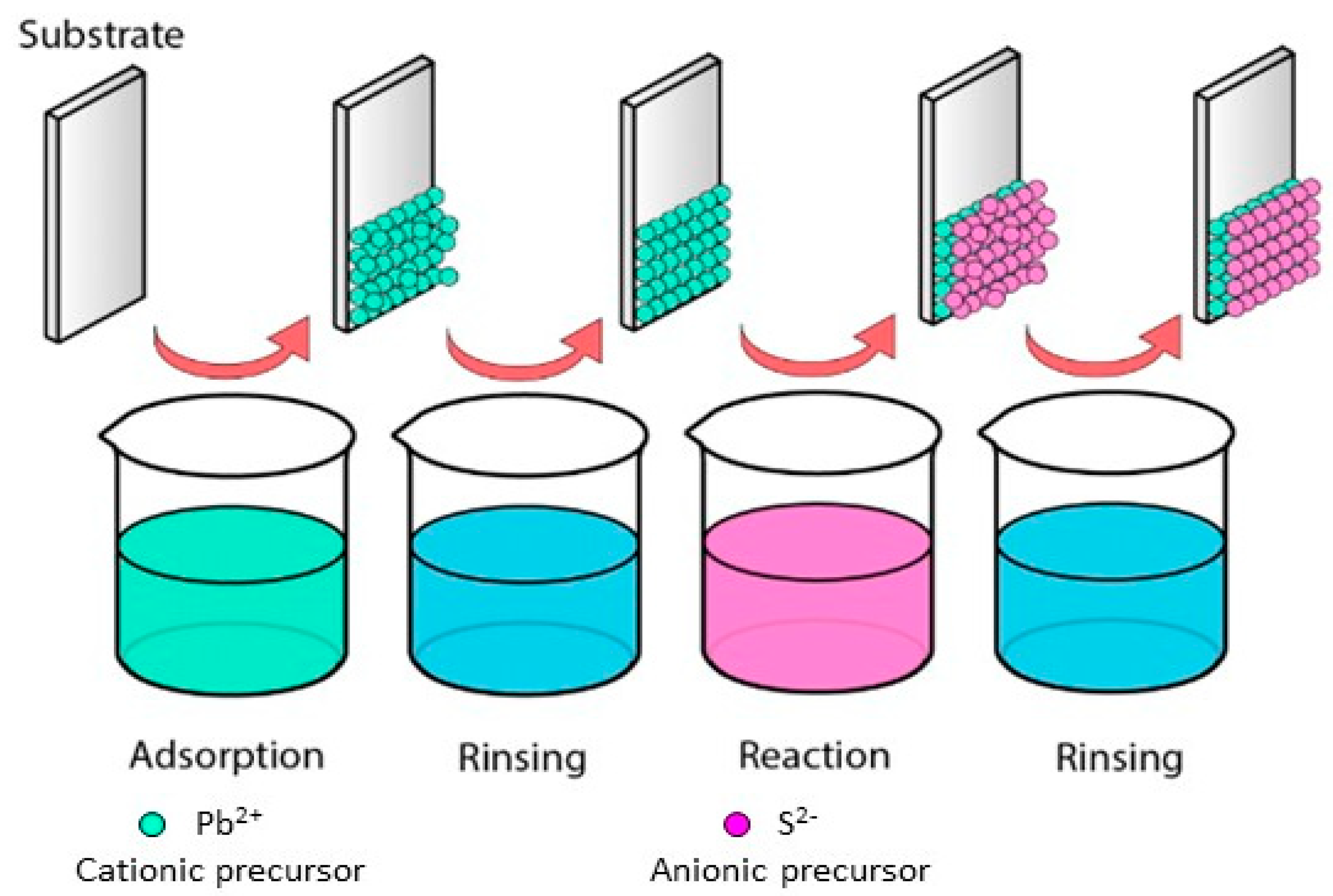
To obtain binary and ternary compound films there are different deposition methods, such as thermal evaporation, immersion, spin coating, pyrolytic spray, and chemical bath deposition. One of the liquid phase methods for the deposition of binary and ternary compounds is the Successive Ionic Layer Adsorption and Reaction (SILAR) method. This method was described by Nicolau [13] and is based on the phenomena of adsorption and reaction of ions from the precursor solutions and the growth of the layers between each immersion, ensuring a homogeneous precipitation of the compound of interest [10]. The precursor solutions of the compound that comprise solvated or complexed ions are placed in different containers: the substrate is immersed in the precursor cationic solution, and subsequently in the precursor anionic solution. The adsorption occurs on the surface between the ions and the substrate surface caused by cohesion forces, Van der Waals forces, or attractive chemical forces. Thus, the residual or unbalanced force allows the adions or molecules to hold on to the substrate’s surface. Factors such as solution temperature, pressure, nature of the substrate, concentration of the solution, and the area of the substrate affect the adsorption process. After each immersion in the cationic and anionic solution, the substrate is rinsed with deionized water to remove the non-adsorbed or unreacted ions at the surface. The reaction of the pre-adsorbed (cations) and freshly adsorbed (anions) ions forms the binary compound of the desired material. A deposition cycle comprises the immersion in the cationic solution, rinsing, immersion in the anionic solution and rinsing. Through the repetition of these cycles, films of binary or ternary compounds are deposited layer by layer [8]. The immersions in the precursor solutions generate layers with nanometer to micrometer thickness, which is controlled with the immersion speed, contact or residence time into the solutions and the number of deposition cycles [13,14]. Figure 1 shows the deposition process of a binary compound by the SILAR method.

Figure 1.
Successive Ionic Layer Adsorption and Reaction process.
The SILAR method has been used to deposit thin films of oxides and binary and ternary chalcogenides and chalcopyrites [12]. This method has advantages such as deposition at room temperature and atmospheric pressure on large areas of different substrates, either insulating, conductor, crystalline, or amorphous; control of the deposition speed and the thickness of the layers by varying the number of cycles; films with good adhesion and homogeneity; as well as high reproducibility.
The available SILAR deposition systems have two degrees of freedom (DOF) along x and y axes. These systems can have a touch screen, connection to a personal computer (PC) or a liquid crystal display (LCD), as well as sensors for temperature and relative humidity measurement, and a microcontroller to assess the impregnation times and number of cycles [15,16,17,18]. However, most of these systems are limited to a maximum of four containers that do not allow as much as binary compound deposition and do not include a mobile app to remotely control and monitor the main performance parameters of the deposition process, which can delay the process several hours, requiring constant user supervision. To overcome these limitations, we propose a simple and low-cost automated device with two DOF to deposit films by the SILAR method. The system contains a mobile app developed in free software code to control of the speeds of the mechanical platform in the directions of the x and y axes, and measures the temperature and relative humidity, as well as the number of cycles and immersion and impregnation times of up to six containers to deposit binary or ternary compound films.
This work is ordered as follows: Section 2 describes the mechanical and electrical elements of the instrument, the implemented logic, and the design of the mobile app; Section 3 explains the deposition and characterization details of lead sulfide (PbS) films with different deposition cycles; finally, the results and discussion of the film characterization by profilometry, Raman spectroscopy, X-ray diffraction and Atomic Force Microscopy to assess the SILAR system performance are presented in Section 4, before the conclusions.
2. Design and Construction of the Instrument
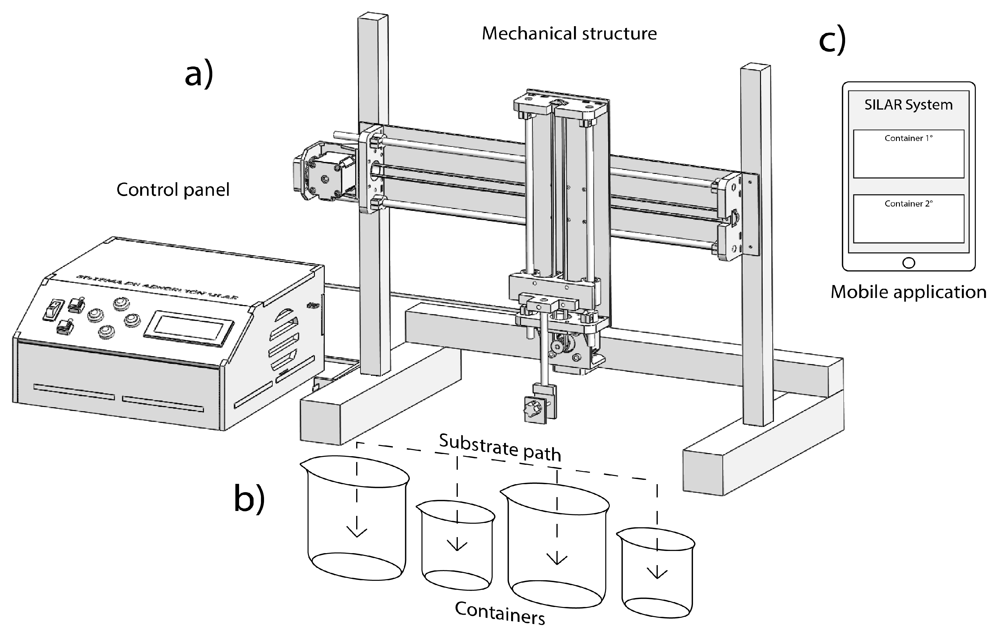
Our automated SILAR instrument, depicted in Figure 2, is formed by three main parts: the mechanical system, the control panel, and the mobile app. This system can move the substrate through trajectories established by the user for each container or beaker, indicating in the control app the capacity of each recipient. However, the containers must be equidistantly placed considering as reference the center of its base, as shown in Figure 2b. The remote control in the mobile app is used to set and monitor the number of the cycles, immersion times and measurement of the sensors, as shown in Figure 2c.
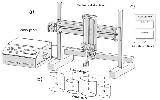
Figure 2.
Automated SILAR device: (a) mechanical system and control panel, (b) displacement along horizontal and vertical axes, and (c) app installed in a mobile device.
2.1. Mechanical System
The mechanical system has a main support structure that ensures the center of gravity within the working area. This system includes galvanized steel posts (44 × 2.5 × 0.3 cm) located at the structure ends and a rectangular metal frame (50 × 10 × 0.5 cm), which provides mechanical stability to the system along the horizontal axis. In addition, a pair of stainless-steel rods in parallel position acts as a guide for a moving platform which displaces in the horizontal (x) and vertical (y) axes. This moving component has two NEMA 17 stepper motors as actuators to generate these displacements. A toothed pulley is placed on each shaft of the motors and together with a toothed belt and a clamp converts the rotary movement to linear displacement. The obtained displacement can be controlled with high precision using micro-steps executed through TB6600 drivers. The relationship between the linear displacement (in centimeters) and the micro-steps is 1:200, i.e., for every 200 micro-steps the displacement is 1 cm. The moving platform has a vertical metal structure (28 × 10 × 0.5 cm) that moves along the rectangular structure of the mechanical system. In the central section of the vertical structure, a toothed pulley and a pair of stainless-steel rods act as displacement guide and support of the vertical structure. In addition, this structure contains a substrate gripper, which is formed by two parallel plates that are perforated in their center with a thread that links them with a threaded screw. Thus, the grip can be adjusted for different substrate thicknesses. Figure 3 depicts the exploded and the assembled view of the components of the mechanical system.
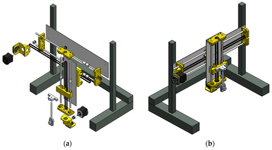
Figure 3.
Design of the mechanical system of the SILAR device: (a) exploded view of the different mechanical elements and (b) view of the assembled mechanical elements.
2.2. Control and Power Stage
Figure 4a shows the block diagram of the electrical and control components of the SILAR device. This system employs an 8-bit microcontroller ATmega2560 (Microchip®) that processes the information for the operation of the actuators, the displacement and speed parameters, execution time, data management, and the reproduction of the routines. The control and heat dissipation elements are distributed within the control panel. Figure 4b illustrates the control panel console, which contains the TB6600 drivers for both stepper motors, the microcontroller, the voltage sources, and a circulation system for air cooling.
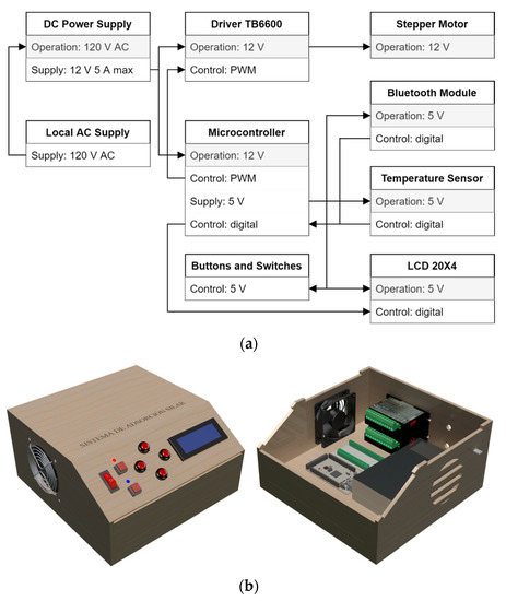
Figure 4.
Automated mechanical system: (a) block diagram of the electrical and control components. (b) Design of the control panel console.
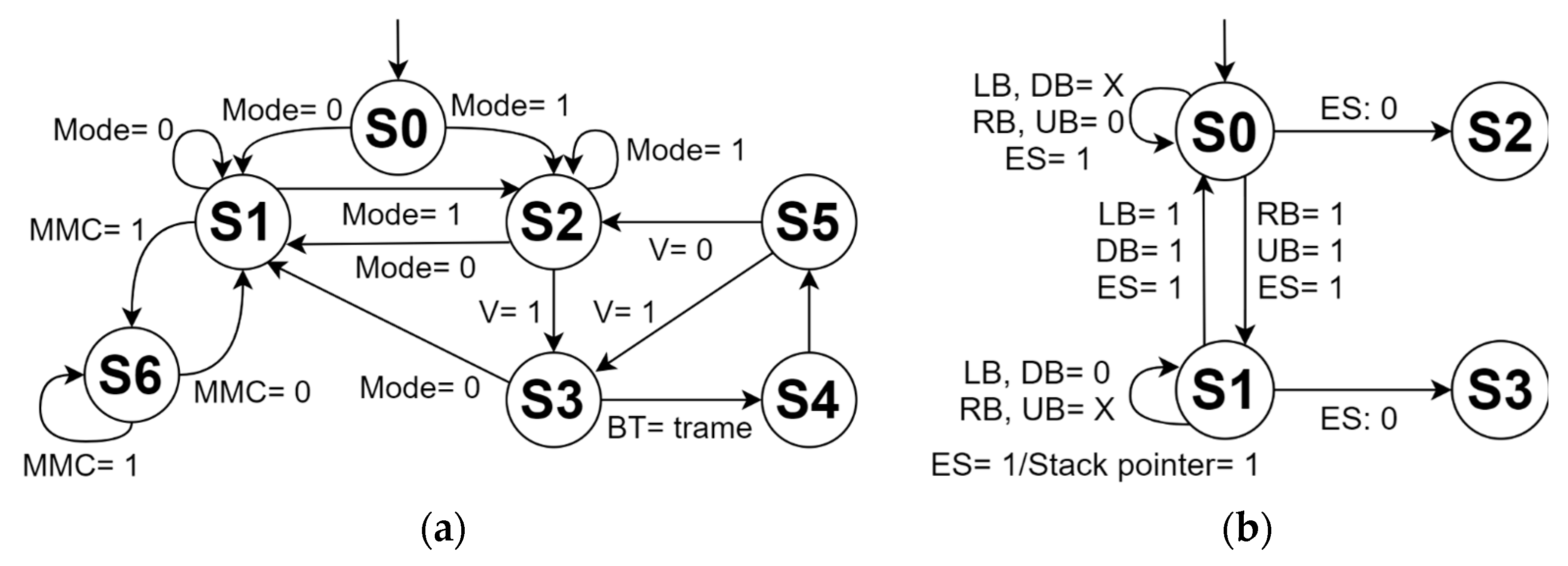
Figure 5a shows the finite-state machine that describes the operation of the mechanical system. First, the system is activated by a main switch and then it is possible to choose the control option through the panel console or the mobile app. Before programming and executing a routine, the control panel console is used to initially verify the operation of the motors, the coupling of the belts, and adjust the moving platform together with the substrate gripper at the origin (machine zero). The second control mode uses a mobile app developed in C++ language installed on a smartphone or tablet, which communicates through the Bluetooth 4.0 protocol with the ATmega2560 microcontroller. During the execution of a routine, it is not possible to manipulate the system through the control panel console. However, there is an emergency stop button on this console, which stops both the movement of the motors and the counts of the internal counters of the routine. Furthermore, the emergency stop indicator LED is activated and the user is informed on the LCD screen about the complete stop of the system. During this state, the user can cancel the routine that is currently running and return to the machine zero position, or can deactivate the emergency stop, continuing the execution of the routine where the system was stopped. The state transition and the inputs and outputs of the operation of the mechanical system are indicated in Table 1 and Table 2, respectively. Figure 5b depicts the finite-state machine of the control panel mode of the mechanical system. S0 represents the emergency stop state, in which the counters, delays, and motors are paused. S1 activates the cancellation of the routine in execution, and S3 places the moving platform in the machine zero position and deletes the routine from the RAM memory of the microcontroller. The state S2 continues executing the routine once the emergency stop is deactivated. The inputs are defined by left button (LB), right button (RB), up button (UB), down button (DB), and emergency stop (ES).
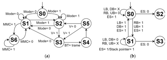
Figure 5.
Finite-state machine of the (a) operation and (b) control panel mode of the automated mechanical system.

Table 1.
Transition states of the finite-state machine for the automated mechanical system.
Table 2.
Inputs and outputs of the operation of the automated mechanical system.
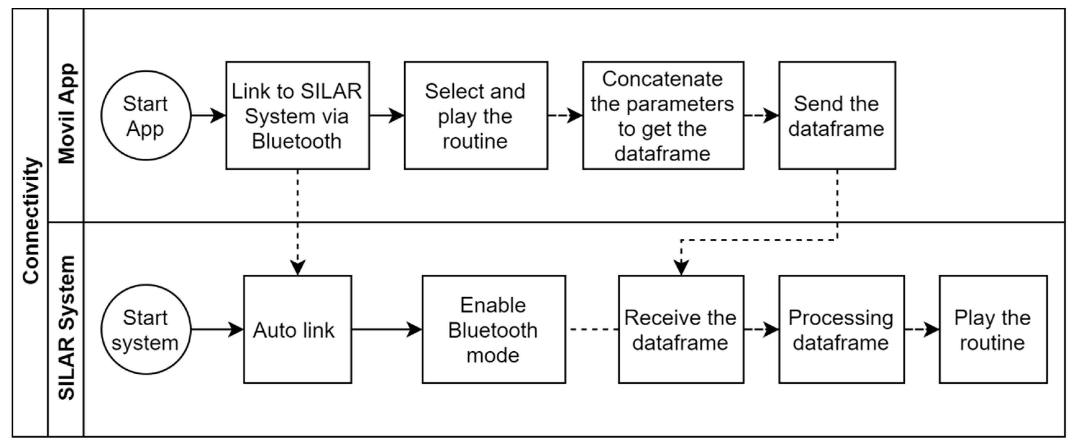
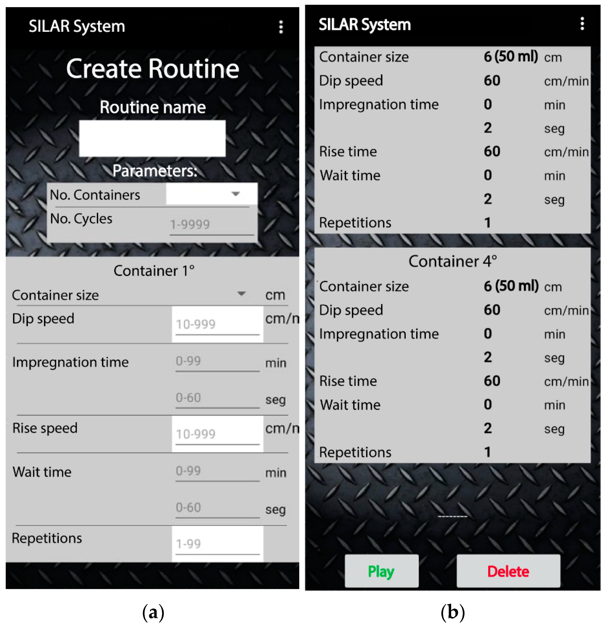
2.3. Mobile Application
The mobile app is the virtual control panel where the user’s routines for binary or ternary film deposition are created, stored, and managed. Each routine is made up of specific parameters, as shown in Figure 6. In a routine, up to six containers of different capacities can be configured for the precursor and rinsing solutions. A data frame is generated in the mobile app with each one of the parameter values selected in the routine. The data frame is sent to the ATmega2560 microcontroller through the Bluetooth communication protocol. Later, the microcontroller processes the data frame by placing each value in significant variables according to the position of each digit in the random-access memory (RAM). Finally, the microcontroller proceeds to execute the routine. Figure 7 represents the connectivity process for the virtual control panel through the mobile app.
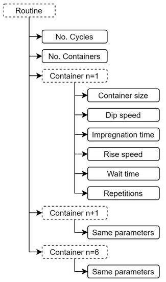
Figure 6.
Specific parameters to be configured by each routine of the virtual control panel of the mechanical system.

Figure 7.
Connectivity between the mobile app and mechanical system based on SILAR method.
The size of the data frame that is sent from the mobile app to the microcontroller depends on the compound type to be deposited and the number of precursor solutions and rinses. Figure 8 shows the structure of the data frame per routine of the mobile app. Table 3 describes the position of the routine parameters placed in the data frame. Table 4 depicts the size of the data frame depending on the number of containers to be used in the SILAR method, ignoring the access code and header bits typical of the Bluetooth protocol [19].
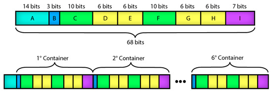
Figure 8.
Structure of the data frame per routine of the mobile app.
Table 3.
Components of the data frame used in the mobile app.
Table 4.
Size of the data frame used in the mobile app in function of the number of used containers.
For the parameter configuration of a routine in the mobile app, the user can visualize the allowed units and quantities for each parameter as seen in Figure 9a. In addition, in the mobile app screen, the operating limits of the different parameters are indicated. The adsorption and wait times can be adjusted in seconds or minutes. Figure 9b shows an example of a previously defined configuration of the parameters required for a binary compound deposition. The mobile app can store up to 100 routines.
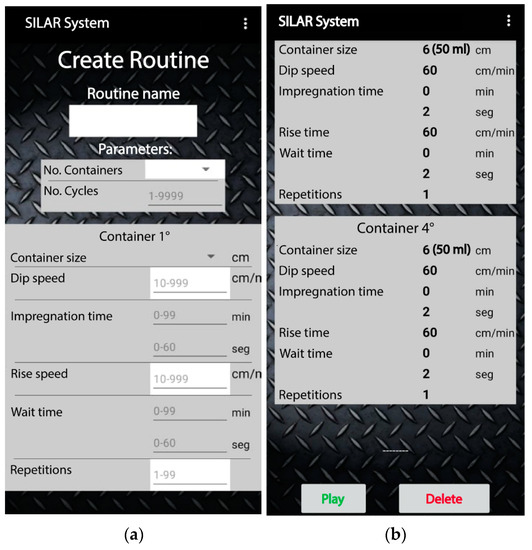
Figure 9.
Graphical user interface of the mobile app: (a) input parameters to create a routine and (b) registered parameters of a sample routine.
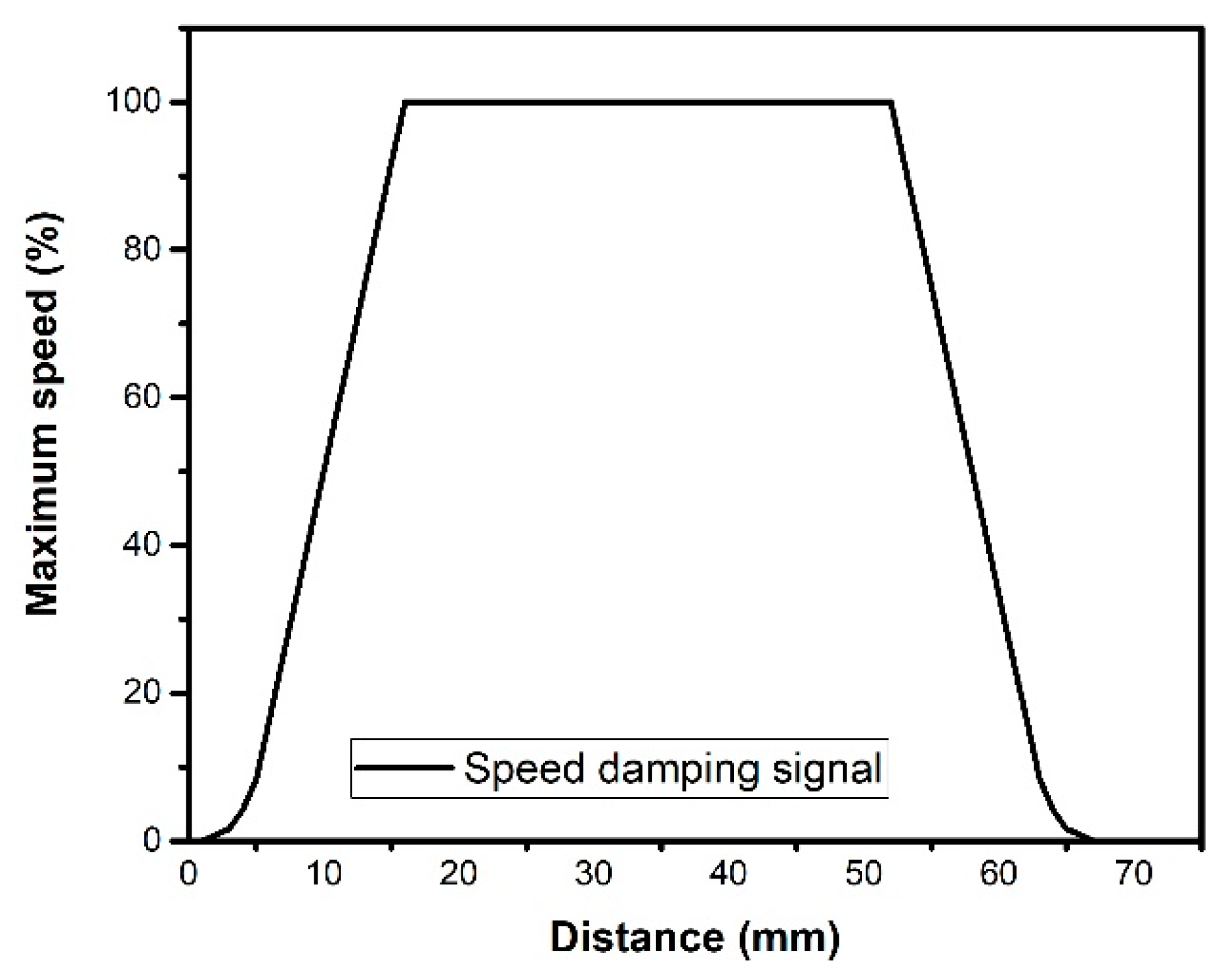
2.4. Acceleration and Deceleration Method
The moving platforms are limited displacements along both the x and y axes. In the x axis, this platform can move up to 53 cm. Thus, the maximum number of steps of the motor is limited to 14,000, starting from the origin position of the moving platform. When the platform stars its movement from this origin point, the position counter increases by 1. On the other hand, if the platform has a movement in the opposite direction, the position counter will decrease by 1 for each step until reaching 0.
A smooth acceleration and deceleration method for the platform was implemented by controlling the timeout from one step to another. To ensure that the platform deceleration starts at 1.5 cm before reaching the desired position, in the value of the deceleration variable the total number of steps is assigned to achieve the displacement minus 600. This behavior of smooth acceleration and deceleration is described by Equation (1):
where A is the new value of the time interval between each of the motor steps, B is the nominal time interval, and C is a constant that varies between 0 to 600 depending on whether the system accelerates or decelerates.
During the start of the motor in the acceleration phase, the variable C is assigned the value of 600. Thus, this initial value of 600 is decreased by 1 for each step reached by the motor, achieving the value 0 for the last step of the motor. For the deceleration, the variable C starts at 0 and increases by 1 for each step of the motor up to 600 in the final position of the platform. Table 5 depicts the effectiveness of the smooth acceleration and deceleration method, reducing the acceleration to gradually obtain the maximum speed of 500 cm min−1.
Table 5.
Values of the variables A and C of Equation (1), in acceleration case, to gradually achieve the speed of 500 cm min−1.
As the motor starts, it has an initial time interval of 3900 μs for each step, obtaining an initial speed of 38.4 cm min−1 of the moving platform in the direction of the x axis. At the end of the start damping, the maximum speed is maintained up to 1.5 cm before reaching the end position, where the deceleration damping is activated. Figure 10 represents the acceleration of the system when it is desired to displace 6.7 cm at maximum speed.

Figure 10.
Percentage of maximum speed of the moving platform considering the distance of 67 mm.
The smooth acceleration and deceleration method is used to decrease the displacement error at each start and stop of the motor. This is due to the stress and inertial force on the toothed belt placed on the vertical motor shaft, which is generated by a load weight close to 1 kg. Thus, the proposed method can decrease the stress on the toothed belt for velocities which overcome 400 cm s−1. For this method, delay times are added because of the speed reduction. Table 6 registers the number of cycles and the deposit time for films of a deposited binary compound, considering the delay time of each routine.
Table 6.
Number of cycles and deposit time for films of a binary compound.
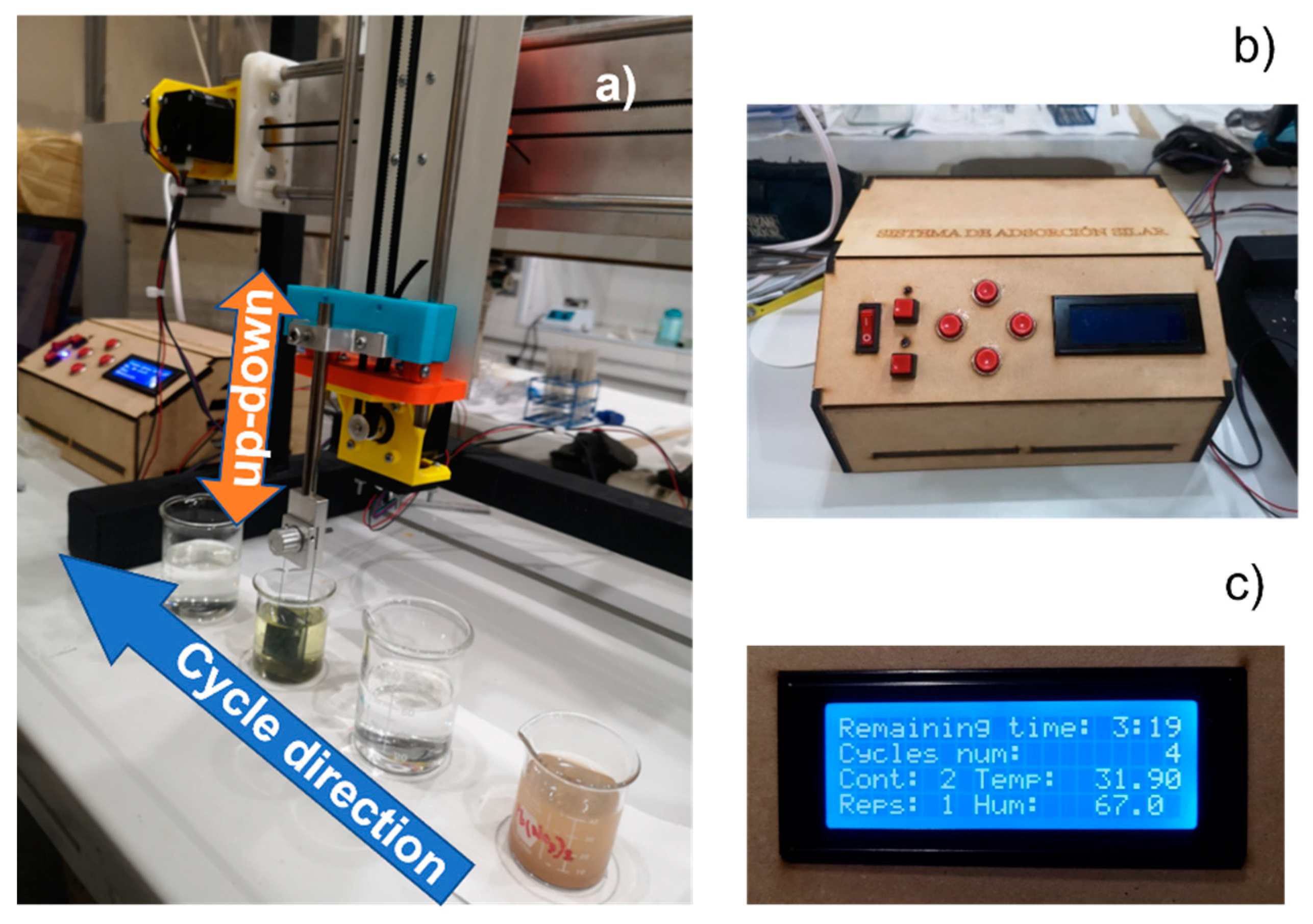
3. Implementation of the Automated Mechanical System
Figure 11 shows the three main parts of the developed SILAR device during the deposition of a PbS film. In the mechanical system (a), the substrate gripper and vertical moving platform are positioned to introduce the substrate into the anionic precursor beaker; the direction of the deposition cycle is indicated with a blue arrow, while the immersion–emersion cycle is depicted with an orange arrow. The control panel console of the system (b) has a digital screen (c) to visualize the parameter values during a routine execution. These data consider the approximate deposition time (in h:min) for a binary or ternary film, the actual cycle number, the container number where the substrate is immersed (1 to 6), the repetition number in which the substrate is found on the same container (Reps), the ambient temperature (in Celsius degrees), and the relative environmental humidity (in %).

Figure 11.
Automated device for thin film deposition by the SILAR method. (a) Support structure, moving platform and solution containers, (b) control panel console, and (c) digital screen of the control panel console.
3.1. PbS Deposition
To assess the operation of the proposed system, PbS films were deposited onto Corning glass substrates with the setup presented in Figure 11 where the substrate was sequentially immersed in four beakers for each cycle in the indicated direction. Before each film deposition, the substrates were cleaned with piranha solution composed by H2O2:H2SO4 (1:1). In this solution, the substrates were immersed and agitated for 5 min. After, the substrates were rinsed with deionized water and later with isopropyl alcohol. Finally, the substrates were reserved in isopropyl alcohol in a closed container.
The cationic precursor solution (Pb2+) was prepared using 0.1 M lead (II) acetate (Pb(CH3COO)2, 99 %, Sigma-Aldrich, St. Louis, MO, USA) and 0.2 M triethanolamine (C6H15NO3 99%, Sigma-Aldrich), in a proportion of 1:2; the anionic solution (S2−) was prepared with 0.1 M thioacetamide (C2H5NS, 99 %, Sigma-Aldrich). The dipping time was 1 min in the cationic solution and anionic solution, respectively, the rinsing time in deionized water was 5 s and the immersion rate was 60 cm/min. The number of deposition cycles was varied from 20 to 500 to study the evolution of the film thickness and crystalline structure.
3.2. Film Characterization
The PbS films were characterized by X-ray diffraction with Cu Kα radiation (λ = 1.5406 Å), in a D8 Advance diffractometer (Bruker) operated at 40 kV and 40 mA in the Bragg–Brentano geometry, in a range 2θ from 10° to 80°, with a step of 0.06°. The Raman spectra were measured using a LabRAM-HR Micro Raman instrument (Horiba Jobin Yvon, Edison, NJ, USA) with a He-Ne laser at 632.8 nm, using neutral density filters to reduce the laser power to avoid damage. Atomic force microscopy images were acquired with a TT AFM instrument (AFM Workshop, Signal Hill, CA, USA) in the non-vibrating mode, using conductive Pt-covered Si tips with a 0.4 N/m constant. Film thickness was measured in a Dektak profilometer (Bruker, Billerica, MA, USA) with a 12 μm stylus, using the edge of the substrate attached to the holder as the required zero-thickness step.
4. Results and Discussion
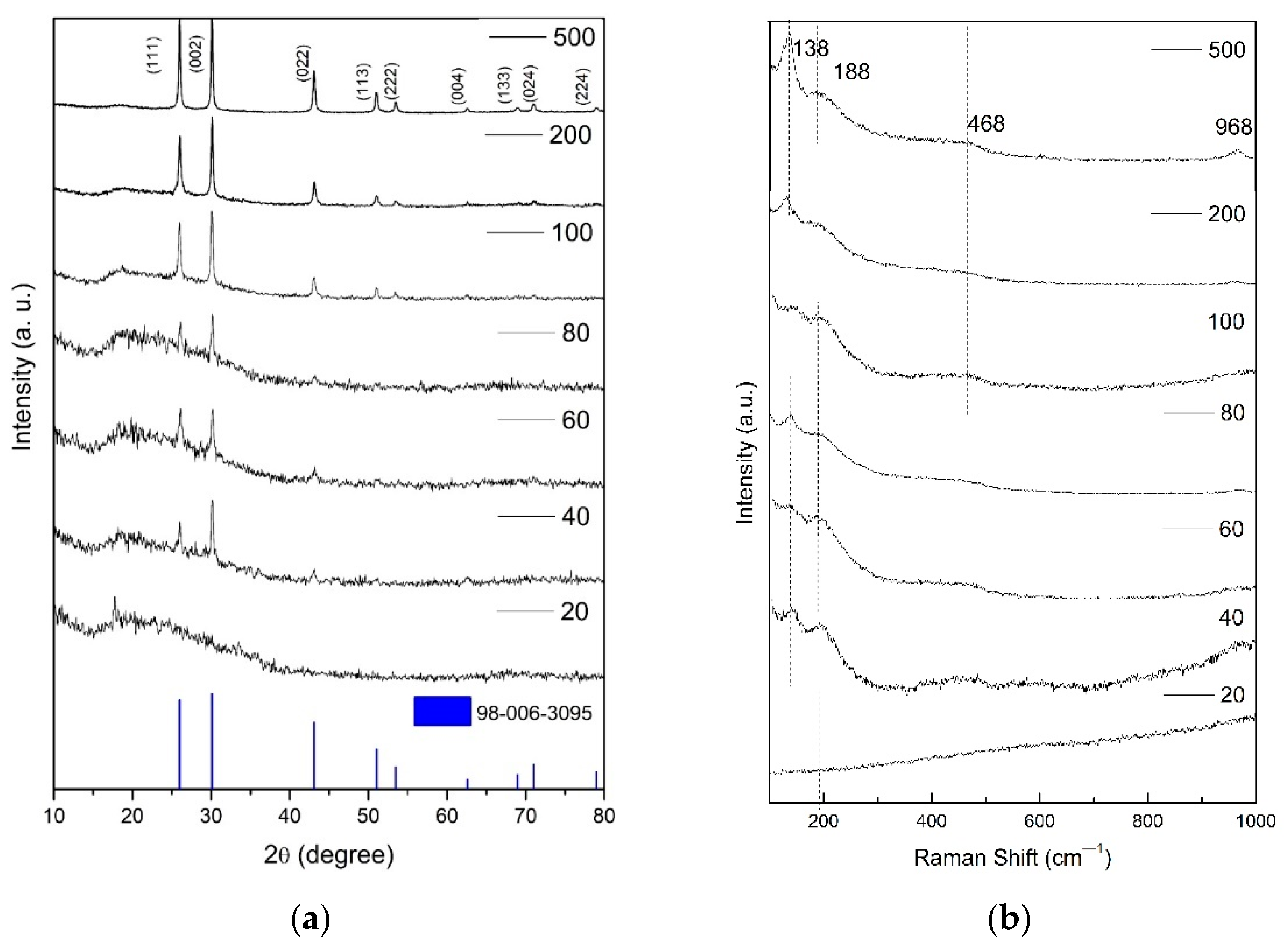
Figure 12a shows the X-ray diffractograms of the PbS films prepared with different deposition cycles. The y-scale of the diffractograms was adapted to better observe the peaks and is not intended to compare the respective peak intensities. The peaks located at 2 theta angles 26.00°, 30.12°, 43.08°, 50.96°, 53.48°, 62.00°, 68.12°, 70.96° and 79.00° correspond to the planes (111), (002), (022), (113), (222), (004), (133), (024) and (224), respectively, of the galene, cubic phase (fcc) of PbS indexing with the PDF Card 98-006-3095 [20]. A non-assigned peak at ca. 18° and a halo between 2 theta 15° and 35° are observed in all the diffractograms. These signals could arise from oxidation of PbS during film deposition or from unreacted precursors. The chemical composition of the samples will be assessed in a future work on the properties of the PbS films and their potential applications. The behavior of the characteristic diffraction peaks shows that the (111) and (002) peaks of PbS develop from 40 deposition cycles, indicating that the in our SILAR device crystalline PbS films can be obtained without further heating. The main peak evolves from (002) to nearly the same intensity of the (111) and (002) planes with the number of deposition cycles. The reduction of the peak width indicates an increasing crystallinity with the number of deposition cycles. A detailed analysis of the evolution of the structure will be presented in a future work.
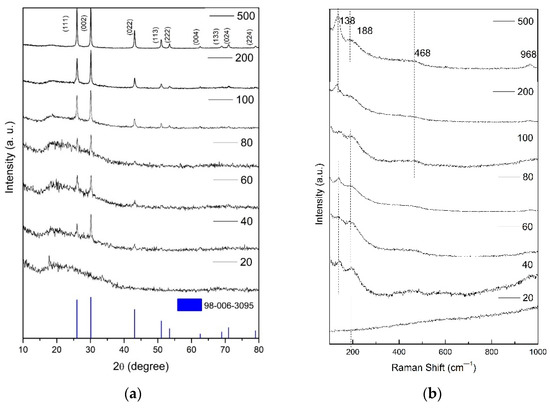
Figure 12.
(a) X-ray diffractograms and (b) Raman spectra of PbS film samples obtained with different number of deposition cycles.
Raman spectra shown in Figure 12b presents peaks at 138, 188, 468 and 968 cm−1. Most of the reports for PbS agreed that 188 and 468 cm−1 Raman peaks come from the combination of the LO–TO modes and to the resonant 2LO overtone induced by Fröhlich interaction, respectively [21,22,23,24,25,26,27]. The peak at 969 cm−1 is due to vibrations in lead sulfates, which the literature attributes to laser decomposition; however, owing to its increased intensity with the number of deposition cycles, we propose that this band arises mostly from surface oxidation during deposition, which could also explain the observed XRD peak at ca. 18º and the halo between 15–35°. Regarding the peak at 138 cm−1, there is some discrepancy in the literature, but considering that the peak we observed at 138 cm−1 increased with the number of cycles, we propose that this peak is related with the formation of large particles onto the continuous film [21,22,23,24,25,26,27], as discussed below in the atomic force characterization. It is interesting to observe that apart from the oxidation after repeated deposition cycles, only peaks attributed to the cubic phase of PbS and those attributed to lead sulfates were observed. As Raman has a good sensitivity to vitreous and nanocrystalline material, it seems reasonable to attribute the non-identified XRD signals to film oxidation products.
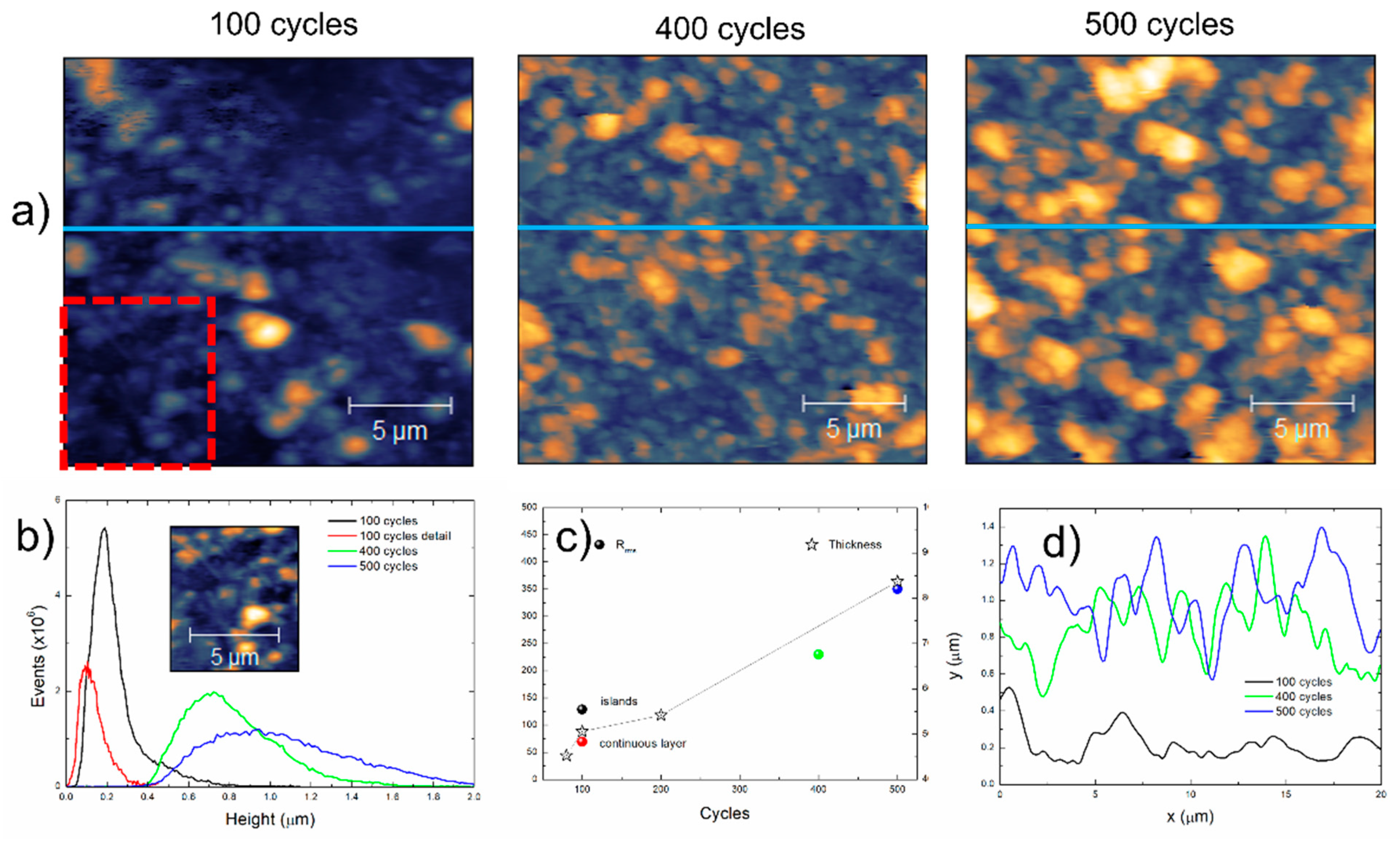
Figure 13 presents the results from the atomic force characterization of the films prepared at 100, 400 and 500 deposition cycles and the comparison with film thickness measured by profilometry.
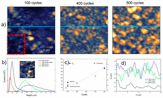
Figure 13.
(a) Presents the 20 × 20 µm2 images, where the increase in surface coverage and apparent grain size are noticeable. (b) Presents the height distribution obtained from the AFM images, as well as from a cropped region marked in a red square from the image of the film prepared with 100 deposition cycles. The maximum height increases from 1.15 µm to 2.07 µm to 2.26 µm with the number of deposition cycles. The maximum height of the cropped region is 454 nm. The behavior of the film prepared with 100 deposition cycles indicates a continuous layer with islands on the top, from single nucleation-growth events [28], while the wide height distributions of the films prepared with 400 and 500 cycles indicate multiple nucleation events with the corresponding growth. (c) Presents the thickness of the films prepared with 80, 100, 200 and 500 deposition cycles measured by stylus profilometry, as well as the root mean square roughness (Rrms) of the films and of the cropped region that confirms that the lower roughness of the “2D” base film increases as islands from subsequent nucleation events grow. It is interesting to observe that the measured film thickness increases from 450 to 840 nm below the observed height maxima of the films (1500 to 2260 nm); this is attributed to the presence of loosely adhered particles that are removed by the stylus with a large tip ratio. The increased roughness of the films prepared at 400 and 500 deposition cycles are a measure of the thickness calculation error and are consequent with the increase in the grain sizes, inferred from the profiles acquired in the images (blue lines) shown in (d).
Thus, the SILAR system allows the preparation of crystalline PbS films with controllable grain size and thickness, although some parameters such as the periodic renovation of the deposition solutions, the residence times into and outside the solutions, the complexing agent concentration, as well as the dipping speed, could be optimized to ensure compact films and reduce the oxidation during deposition. A future in situ diagnostic system is intended using remote sensing Raman spectroscopy to assess the evolution in film microstructure during deposition.
5. Conclusions
A simple automated device with two degrees of freedom for the deposition of thin films based on the SILAR method was developed. This system is integrated by a support structure and a moving platform, a control panel console, and an app that can be integrated in a mobile device, to control the different operation parameters of the instrument. Thus, the deposition process of thin films is controlled by the users, ensuring good homogeneous deposition kinematics without capillarity problems due to vibrations of the actuators. The performance of the device was studied by depositing PbS films from 20 to 500 cycles and studying the evolution of the thickness, structure, and morphology of the deposited films. Crystalline, cubic PbS films were obtained from 40 deposition cycles, although due to the non-optimized deposition parameters, some film oxidation during deposition was observed. Raman and AFM indicate that films grew in a mixed mode, i.e., a continuous film with islands on the top. The results indicate that the developed instrument is suitable to operate automatically, supervised from a mobile device, up to 500 deposition cycles (ca. 15 h), producing films with good crystallinity and controllable thickness and grain size. Further experiments for depositing other materials and the optimization of the deposition parameters including the bath formulations and cycle programming are intended.
Author Contributions
R.M.W.-G., I.R.-I., E.O.-d.-l.-R. and R.A.-S., designed and implemented the SILAR system; R.M.W.-G., I.R.-I. and C.G.-A. prepared the films; F.C.-B. and C.G.-A. analyzed the XRD, Raman and AFM results; A.L.H.-M., F.C.-B., C.G.-A. and F.L.-H. wrote and corrected the manuscript. All authors have read and agreed to the published version of the manuscript.
Funding
Financed through the CONACyT CB-2016-286059 and CdF-2019-40798 projects.
Acknowledgments
R.M.W.-G. and I.R.-I. thank CONACyT for the scholarships 588062 and 1138397. Laboratorio Central del Instituto de Física “Ing. Luis Rivera Terrazas”–BUAP is acknowledged for the Micro Raman and profilometry measurements. Technical assistance from S. Pacheco in XRD acquisition and from F. Ruiz-Perez in AFM imaging is granted thanks as well.
Conflicts of Interest
The authors declare no conflict of interest.
References
- Znaidi, L. Sol–gel-deposited ZnO thin films: A review. Mater. Sci. Eng. B 2010, 174, 18–30. [Google Scholar] [CrossRef]
- Delbos, S. Kësterite thin films for photovoltaics: A review. EPJ Photovolt. 2012, 3, 35004. [Google Scholar] [CrossRef]
- Lee, H.J.; Bang, J.; Park, J.; Kim, S.; Park, S.-M. Multilayered semiconductor (CdS/CdSe/ZnS)-sensitized TiO2 mesoporous solar cells: All prepared by successive ionic layer adsorption and reaction processes. Chem. Mater. 2010, 22, 5636–5643. [Google Scholar] [CrossRef]
- Garcia-Garcia, F.J.; Gil-Rostra, J.; Terriza, A.; González, J.C.; Cotrino, J.; Frutos, F.; Ferrer, F.J.; González-Elipe, A.R.; Yubero, F. Low refractive index SiOF thin films prepared by reactive magnetron sputtering. Thin Solid Films 2013, 542, 332–337. [Google Scholar] [CrossRef]
- Garcia-Garcia, F.J.; Beltrán, A.M.; Yubero, F.; González-Elipe, A.R.; Lambert, R.M. High performance novel gadolinium doped ceria/yttria stabilized zirconia/nickel layered and hybrid thin film anodes for application in solid oxide fuel cells. J. Power Sources 2017, 363, 251–259. [Google Scholar] [CrossRef] [Green Version]
- Desai, M.A.; Sharma, V.; Prasad, M.; Jadkar, S.; Saratale, G.D.; Sartale, S.D. Seed-layer-free deposition of well-oriented ZnO nanorods thin films by SILAR and their photoelectrochemical studies. Int. J. Hydrogen Energy 2020, 45, 5783–5792. [Google Scholar] [CrossRef]
- Sfaelou, S.; Sygellou, L.; Dracopoulos, V.; Travlos, A.; Lianos, P. Effect of the nature of cadmium salts on the effectiveness of CdS SILAR deposition and its consequences on the performance of sensitized solar cells. J. Phys. Chem. C 2014, 118, 22873–22880. [Google Scholar] [CrossRef]
- Das, M.R.; Roy, A.; Mpelane, S.; Mukherjee, A.; Mitra, P.; Das, S. Influence of dipping cycle on SILAR synthesized NiO thin film for improved electrochemical performance. Electrochim. Acta 2018, 273, 105–114. [Google Scholar] [CrossRef]
- Khan, M.; Irfan, M.H.; Israr, M.; Rehman, N.; Park, T.J.; Basit, M.A. Comparative investigation of ZnO morphologies for optimal CdS quantum-dot deposition via pseudo-SILAR method. Chem. Phys. Lett. 2020, 744, 137223. [Google Scholar] [CrossRef]
- Abdulrahman, A.F.; Abd-Alghafour, N.M.; Ahmed, S.M. Optimization and characterization of SILAR synthesized ZnO nanorods for UV photodetector sensor. Sens. Actuators A Phys. 2021, 323, 112656. [Google Scholar] [CrossRef]
- Nicolau, Y.F. Solution deposition of thin solid compound films by a successive ionic-layer adsorption and reaction process. Appl. Surf. Sci. 1985, 22, 1061–1074. [Google Scholar] [CrossRef]
- Da Silva-Filho, J.M.C.; Marques, F.C. Structural and optical temperature-dependent properties of PbS thin films deposited by radio frequency sputtering. Mater. Sci. Semicond. Process. 2019, 91, 188–193. [Google Scholar] [CrossRef]
- Pathan, H.M.; Lokhande, C.D. Deposition of metal chalcogenide thin films by successive ionic layer adsorption and reaction (SILAR) method. Bull. Mater. Sci. 2004, 27, 85–111. [Google Scholar] [CrossRef]
- Mageshwari, K.; Sathyamoorthy, R. Physical properties of nanocrystalline CuO thin films prepared by the SILAR method. Mater. Sci. Semicond. Process. 2013, 16, 337–343. [Google Scholar] [CrossRef]
- Yücel, E.; Yücel, Y.; Beleli, B. Process optimization of deposition conditions of PbS thin films grown by a successive ionic layer adsorption and reaction (SILAR) method using response surface methodology. J. Cryst. Growth 2015, 422, 1–7. [Google Scholar] [CrossRef]
- Calixto-Rodriguez, M.; Valdez Martínez, J.S.; Meneses-Arcos, M.A.; Ortega-Cruz, J.; Sarmiento-Bustos, E.; Reyes-Mayer, A.; González-Castañeda, M.; Domínguez García, R.O. Design and Development of Software for the SILAR Control Process Using a Low-Cost Embedded System. Processes 2021, 9, 967. [Google Scholar] [CrossRef]
- Garzón-Ramos, D.A.; Martínez, A.; Rico, D.; Guzmán-Embús, D.A.; Vargas-Hernández, C. Silar system to growth of semiconductor films with different applications. Rev. Investig. Univ. Quindío 2012, 23, 16–22. [Google Scholar] [CrossRef]
- Valdez-Martínez, J.S.; Meneses-Arcos, M.A.; Calixto-Rodriguez, M.; Rumbo-Morales, J.Y.; Beltran-Escobar, M.A.; Villanueva-Tavira, J.; Sarmiento-Bustos, E. Automation of the successive ionic layer adsorption and reaction-SILAR-process. Rev. Mex. De Ing. Química 2020, 19, 1351–1361. [Google Scholar] [CrossRef]
- Darroudi, S.M.; Gomez, C. Bluetooth Low Energy Mesh Networks: A Survey. Sensors 2017, 17, 1467. [Google Scholar] [CrossRef] [PubMed] [Green Version]
- Judita, P.; Sigitas, T.; Giedrius, L.; Lindroos, S.; Markku, L.; Valentinas, S. Growth of PbS thin films on silicon substrate by SILAR technique. Thin Solid Films 2002, 403, 457–461. [Google Scholar] [CrossRef]
- Jian, P.G.; Jin, W.; Hao, X.Z.; Xun, W.; Qing, P.; Ya, D.L. Orthogonal PbS nanowire arrays and networks and their Raman scattering behavior. Chem. Eur. J. 2005, 11, 1889–1894. [Google Scholar] [CrossRef]
- Mohsen, C.; Ramin, Y.; Farid, J.S.; Abdolhossein, S. Comparative study of Raman properties of various lead sulfide morphologies. Majlesi J. Telecommun. Devices 2013, 2, 163–166. [Google Scholar]
- Bai, H.; Li, X.; Guo, F.; Zhang, B.; Yang, Q.; Zhang, L.; Song, Y.; Huang, Y. Comparative study on the growth mechanism of multi-shaped PbS via hydro- and solvothermal methods. Opt. Mater. Express 2019, 9, 932–943. [Google Scholar] [CrossRef]
- Fekadu, G.H.; Dejene, F.B. Six complexing agents and their effects on optical, structural, morphological and photoluminescence properties of lead sulphide thin films prepared by chemical route. J. Luminescence 2018, 201, 321–328. [Google Scholar] [CrossRef]
- Gregory, D.S.; Steven, F.; Robin, J.H.C.; Manuel, C. First- and second-order Raman spectra of galena (PbS). J. Appl. Phys. 2002, 92, 4375. [Google Scholar] [CrossRef]
- Etchegoin, P.; Manuel, C.; Lauck, R.; Clark, R.; Serrano, J.; Romero, A.H. Temperature-dependent Raman scattering of natural and isotopically substituted PbS. Phys. Stat. Sol. 2008, 245, 1125–1132. [Google Scholar] [CrossRef] [Green Version]
- Bencherif, Y.; Boukra, A.; Zaoui, A.; Ferhat, M. Lattice dynamics study of leads chalcogenides. Infrared Phys. Technol. 2011, 54, 39–43. [Google Scholar] [CrossRef]
- Resch, R.; Friedbacher, G.; Grasserbauer, M.; Kanniainen, T.; Lindroos, S.; Leskelä, M.; Niinistö, L. Lateral force microscopy and force modulation microscopy on SILAR-grown lead sulfide samples. Appl. Surf. Sci. 1997, 120, 51–57. [Google Scholar] [CrossRef]


Publisher’s Note: MDPI stays neutral with regard to jurisdictional claims in published maps and institutional affiliations. |
© 2022 by the authors. Licensee MDPI, Basel, Switzerland. This article is an open access article distributed under the terms and conditions of the Creative Commons Attribution (CC BY) license (https://creativecommons.org/licenses/by/4.0/).