
A Review of the Impact of Zinc Oxide Nanostructure Morphology on Perovskite Solar Cell Performance
 , , , and
Abstract
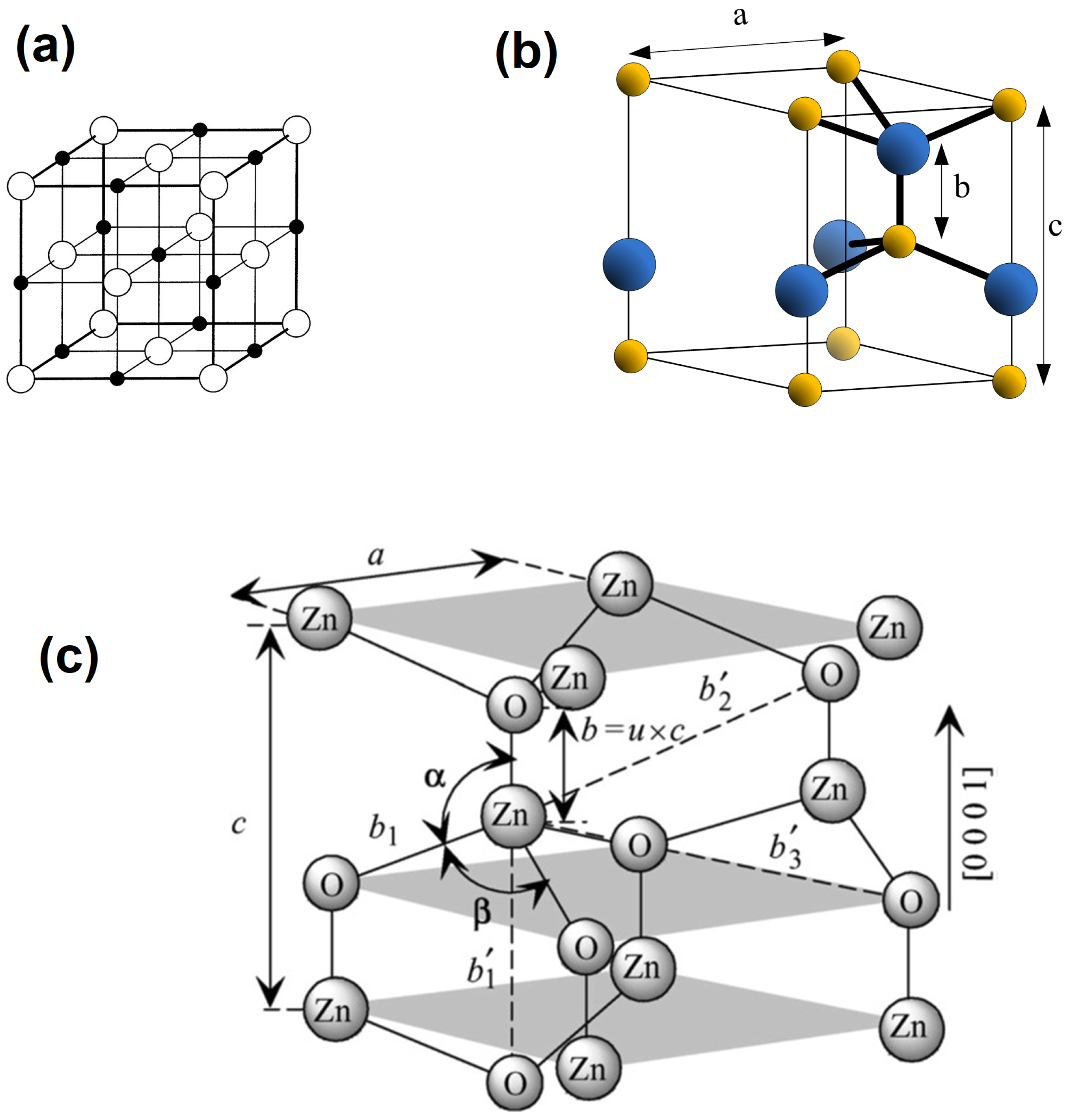
:1. Introduction
Application of ZnO Nanostructures in Perovskite Solar Cells
2. Synthesis Routes for ZnO Nanostructures
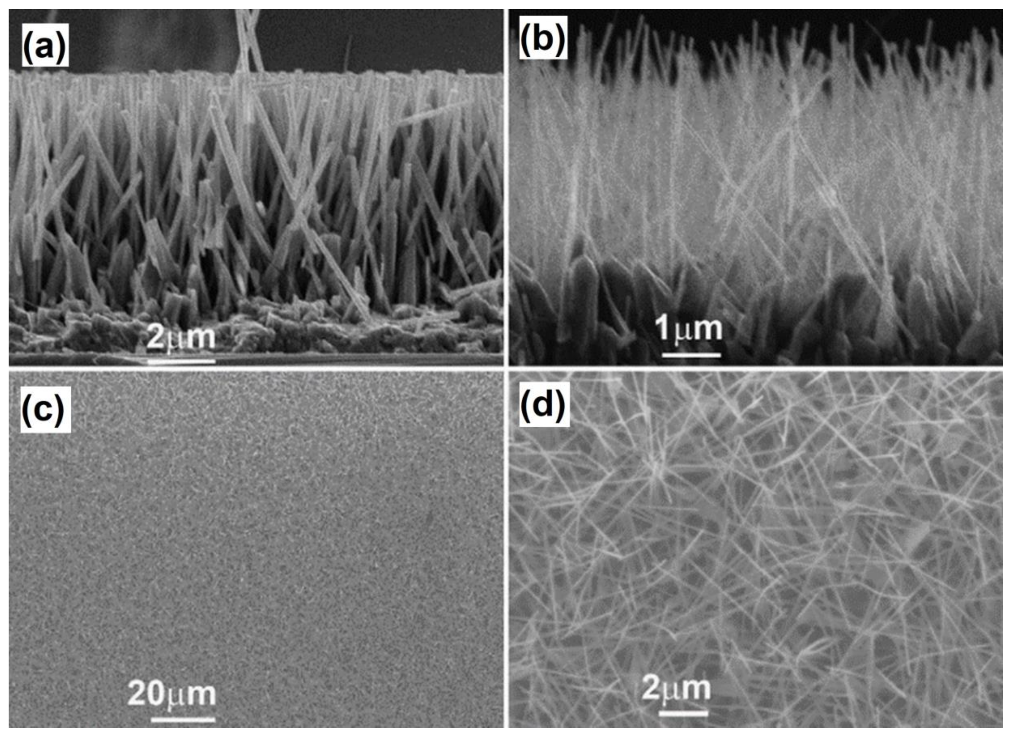
2.1. Hydrothermal Synthesis of ZnO Nanostructures
2.2. Sol–Gel Synthesis of ZnO nanostructures
2.3. Chemical Bath Deposition Synthesis of ZnO Nanostructures
2.4. Physical Vapour Deposition Synthesis of ZnO Nanostructures
2.5. Plant Extract Synthesis of ZnO Nanostructures
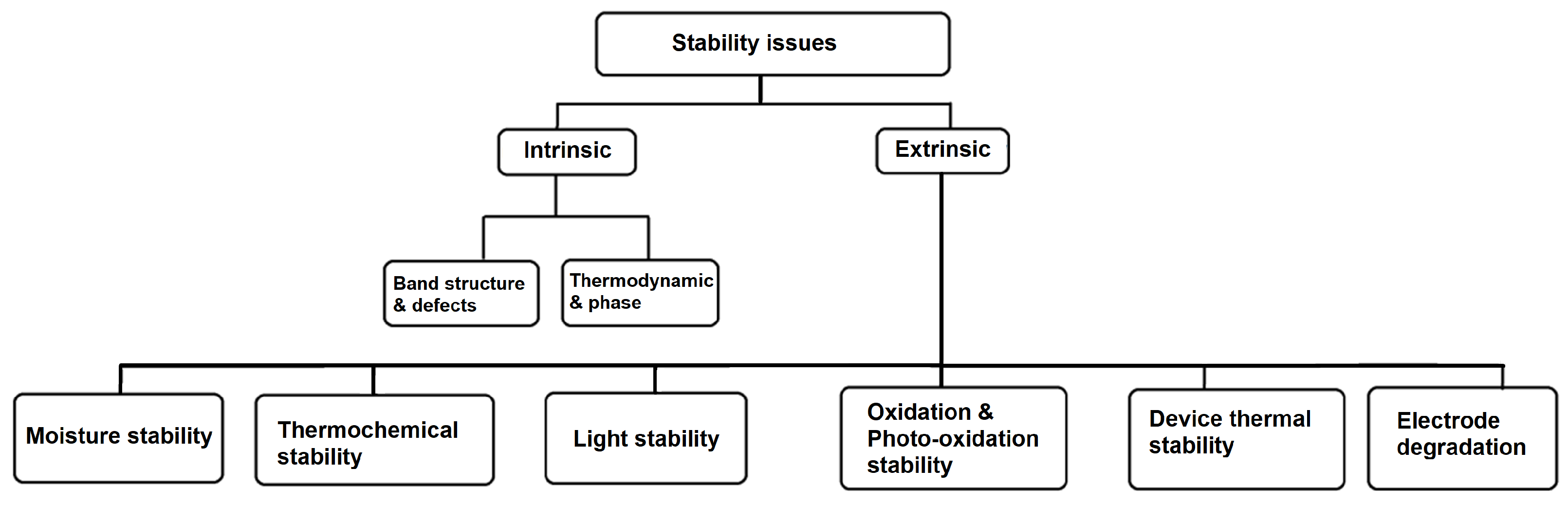
3. Challenges and Future Directions of ZnO-Based PSCs
4. Conclusions
Author Contributions
Funding
Institutional Review Board Statement
Informed Consent Statement
Data Availability Statement
Conflicts of Interest
References
- Mahmood, K.; Swain, B.S.; Amassian, A. Double-layered ZnO nanostructures for efficient perovskite solar cells. Nanoscale 2014, 6, 14674–14678. [Google Scholar] [CrossRef] [PubMed]
- Xu, F.; Dai, M.; Lu, Y.; Sun, L. Hierarchical ZnO nanowire- nanosheet architectures for high power conversion efficiency in dye-sensitized solar cells. J. Phys. Chem. C 2010, 114, 2776–2782. [Google Scholar] [CrossRef]
- Feng, Y.; Ji, X.; Duan, J.; Zhu, J.; Jiang, J.; Ding, H.; Meng, G.; Ding, R.; Liu, J.; Hu, A.; et al. Synthesis of ZnO@ TiO2 core–shell long nanowire arrays and their application on dye-sensitized solar cells. J. Solid State Chem. 2012, 190, 303–308. [Google Scholar] [CrossRef]
- Djurišić, A.B.; Leung, Y.H. Optical properties of ZnO nanostructures. Small 2006, 2, 944–961. [Google Scholar] [CrossRef] [PubMed]
- Pal, U.; Serrano, J.G.; Santiago, P.; Xiong, G.; Ucer, K.; Williams, R. Synthesis and optical properties of ZnO nanostructures with different morphologies. Opt. Mater. 2006, 29, 65–69. [Google Scholar] [CrossRef]
- Fodjouong, G.J.; Feng, Y.; Sangare, M.; Huang, X. Synthesis of ZnO nanostructure films by thermal evaporation approach and their application in dye-sensitized solar cells. Mater. Sci. Semicond. Process. 2013, 16, 652–658. [Google Scholar] [CrossRef]
- Li, D.; Haneda, H. Morphologies of zinc oxide particles and their effects on photocatalysis. Chemosphere 2003, 51, 129–137. [Google Scholar] [CrossRef]
- Duan, J.; Xiong, Q.; Wang, H.; Zhang, J.; Hu, J. ZnO nanostructures for efficient perovskite solar cells. J. Mater. Sci. Mater. Electron. 2017, 28, 60–66. [Google Scholar] [CrossRef]
- Galdámez-Martinez, A.; Santana, G.; Güell, F.; Martínez-Alanis, P.R.; Dutt, A. Photoluminescence of ZnO nanowires: A review. Nanomaterials 2020, 10, 857. [Google Scholar] [CrossRef]
- Shouli, B.; Liangyuan, C.; Dianqing, L.; Wensheng, Y.; Pengcheng, Y.; Zhiyong, L.; Aifan, C.; Liu, C.C. Different morphologies of ZnO nanorods and their sensing property. Sensors Actuators B Chem. 2010, 146, 129–137. [Google Scholar] [CrossRef]
- Fakharuddin, A.; Di Giacomo, F.; Ahmed, I.; Wali, Q.; Brown, T.M.; Jose, R. Role of morphology and crystallinity of electron transport layer on long term durable performance of perovskite solar cells. J. Power Sources 2015, 283, 61–67. [Google Scholar] [CrossRef]
- Tang, J.F.; Tseng, Z.L.; Chen, L.C.; Chu, S.Y. ZnO nanowalls grown at low-temperature for electron collection in high-efficiency perovskite solar cells. Sol. Energy Mater. Sol. Cells 2016, 154, 18–22. [Google Scholar] [CrossRef]
- Han, G.S.; Shim, H.W.; Lee, S.; Duff, M.L.; Lee, J.K. Low-Temperature Modification of ZnO Nanoparticles Film for Electron-Transport Layers in Perovskite Solar Cells. ChemSusChem 2017, 10, 2425–2430. [Google Scholar] [CrossRef]
- Leonardi, S.G. Two-dimensional zinc oxide nanostructures for gas sensor applications. Chemosensors 2017, 5, 17. [Google Scholar] [CrossRef]
- Schutt, K.; Nayak, P.K.; Ramadan, A.J.; Wenger, B.; Lin, Y.H.; Snaith, H.J. Overcoming zinc oxide interface instability with a methylammonium-free perovskite for high-performance solar cells. Adv. Funct. Mater. 2019, 29, 1900466. [Google Scholar] [CrossRef]
- Mohamed Saheed, M.S.; Mohamed, N.M.; Singh, B.S.M.; Saheed, M.S.M.; Jose, R. Optoelectronic Enhancement of Perovskite Solar Cells through the Incorporation of Plasmonic Particles. Micromachines 2022, 13, 999. [Google Scholar] [CrossRef]
- Pitchaiya, S.; Eswaramoorthy, N.; Natarajan, M.; Santhanam, A.; Ramakrishnan, V.M.; Asokan, V.; Palanichamy, P.; Palanisamy, B.; Kalimuthu, A.; Velauthapillai, D. Interfacing green synthesized flake like-ZnO with TiO2 for bilayer electron extraction in perovskite solar cells. New J. Chem. 2020, 44, 8422–8433. [Google Scholar] [CrossRef]
- Luo, J.; Wang, Y.; Zhang, Q. Progress in perovskite solar cells based on ZnO nanostructures. Solar Energy 2018, 163, 289–306. [Google Scholar] [CrossRef]
- Li, S.; Zhang, P.; Chen, H.; Wang, Y.; Liu, D.; Wu, J.; Sarvari, H.; Chen, Z.D. Mesoporous PbI2 assisted growth of large perovskite grains for efficient perovskite solar cells based on ZnO nanorods. J. Power Sources 2017, 342, 990–997. [Google Scholar] [CrossRef]
- Eswaramoorthy, N.; Kamatchi, R. Planar perovskite solar cells: Eco-friendly synthesized cone-like ZnO nanostructure for efficient interfacial electron transport layer. J. Mater. Sci. Mater. Electron. 2021, 32, 24138–24151. [Google Scholar] [CrossRef]
- Zeng, J.; Qi, Y.; Liu, Y.; Chen, D.; Ye, Z.; Jin, Y. ZnO-Based Electron-Transporting Layers for Perovskite Light-Emitting Diodes: Controlling the Interfacial Reactions. J. Phys. Chem. Lett. 2022, 13, 694–703. [Google Scholar] [CrossRef] [PubMed]
- Yang, G.; Tao, H.; Qin, P.; Ke, W.; Fang, G. Recent progress in electron transport layers for efficient perovskite solar cells. J. Mater. Chem. A 2016, 4, 3970–3990. [Google Scholar] [CrossRef]
- Zhou, H.; Yang, L.; Gui, P.; Grice, C.R.; Song, Z.; Wang, H.; Fang, G. Ga-doped ZnO nanorod scaffold for high-performance, hole-transport-layer-free, self-powered CH3NH3PbI3 perovskite photodetectors. Sol. Energy Mater. Sol. Cells 2019, 193, 246–252. [Google Scholar] [CrossRef]
- Kojima, A.; Teshima, K.; Shirai, Y.; Miyasaka, T. Organometal halide perovskites as visible-light sensitizers for photovoltaic cells. J. Am. Chem. Soc. 2009, 131, 6050–6051. [Google Scholar] [CrossRef]
- Luo, L.; Lv, G.; Li, B.; Hu, X.; Jin, L.; Wang, J.; Tang, Y. Formation of aligned ZnO nanotube arrays by chemical etching and coupling with CdSe for photovoltaic application. Thin Solid Films 2010, 518, 5146–5152. [Google Scholar] [CrossRef]
- Zhao, J.; Zheng, X.; Deng, Y.; Li, T.; Shao, Y.; Gruverman, A.; Shield, J.; Huang, J. Is Cu a stable electrode material in hybrid perovskite solar cells for a 30-year lifetime? Energy Environ. Sci. 2016, 9, 3650–3656. [Google Scholar] [CrossRef]
- Dong, J.; Shi, J.; Li, D.; Luo, Y.; Meng, Q. Controlling the conduction band offset for highly efficient ZnO nanorods based perovskite solar cell. Appl. Phys. Lett. 2015, 107, 073507. [Google Scholar] [CrossRef]
- Khan, F.; Kim, J.H. Enhanced charge-transportation properties of low-temperature processed Al-doped ZnO and its impact on PV cell parameters of organic-inorganic perovskite solar cells. Solid-State Electron. 2020, 164, 107714. [Google Scholar] [CrossRef]
- Nagarjuna, Y.; Hsiao, Y.J. Au doping ZnO nanosheets sensing properties of ethanol gas prepared on MEMS device. Coatings 2020, 10, 945. [Google Scholar] [CrossRef]
- Kumar, M.H.; Yantara, N.; Dharani, S.; Graetzel, M.; Mhaisalkar, S.; Boix, P.P.; Mathews, N. Flexible, low-temperature, solution processed ZnO-based perovskite solid state solar cells. Chem. Commun. 2013, 49, 11089–11091. [Google Scholar] [CrossRef]
- Bi, D.; Boschloo, G.; Schwarzmüller, S.; Yang, L.; Johansson, E.M.; Hagfeldt, A. Efficient and stable CH3NH3PbI3-sensitized ZnO nanorod array solid-state solar cells. Nanoscale 2013, 5, 11686–11691. [Google Scholar] [CrossRef]
- Zuo, L.; Gu, Z.; Ye, T.; Fu, W.; Wu, G.; Li, H.; Chen, H. Enhanced photovoltaic performance of CH3NH3PbI3 perovskite solar cells through interfacial engineering using self-assembling monolayer. J. Am. Chem. Soc. 2015, 137, 2674–2679. [Google Scholar] [CrossRef]
- Zhuiykov, S. Nanostructured Semiconductor Oxides for the Next Generation of Electronics and Functional Devices: Properties and Applications; Woodhead Publishing: Sawston, UK, 2014. [Google Scholar]
- Xu, Y.; Liu, T.; Li, Z.; Feng, B.; Li, S.; Duan, J.; Ye, C.; Zhang, J.; Wang, H. Preparation and photovoltaic properties of perovskite solar cell based on ZnO nanorod arrays. Appl. Surf. Sci. 2016, 388, 89–96. [Google Scholar] [CrossRef]
- Son, D.Y.; Im, J.H.; Kim, H.S.; Park, N.G. 11% efficient perovskite solar cell based on ZnO nanorods: An effective charge collection system. J. Phys. Chem. C 2014, 118, 16567–16573. [Google Scholar] [CrossRef]
- Dong, J.; Zhao, Y.; Shi, J.; Wei, H.; Xiao, J.; Xu, X.; Luo, J.; Xu, J.; Li, D.; Luo, Y.; et al. Impressive enhancement in the cell performance of ZnO nanorod-based perovskite solar cells with Al-doped ZnO interfacial modification. Chem. Commun. 2014, 50, 13381–13384. [Google Scholar] [CrossRef]
- Zheng, Y.; Zhao, E.; Meng, F.; Lai, X.; Dong, X.; Wu, J.; Tao, X. Iodine-doped ZnO nanopillar arrays for perovskite solar cells with high efficiency up to 18.24%. J. Mater. Chem. 2017, 5, 12416–12425. [Google Scholar] [CrossRef]
- Wibowo, A.; Marsudi, M.A.; Amal, M.I.; Ananda, M.B.; Stephanie, R.; Ardy, H.; Diguna, L.J. ZnO nanostructured materials for emerging solar cell applications. RSC Adv. 2020, 10, 42838–42859. [Google Scholar] [CrossRef]
- Dehghan, M.; Behjat, A. Deposition of zinc oxide as an electron transport layer in planar perovskite solar cells by spray and SILAR methods comparable with spin coating. RSC Adv. 2019, 9, 20917–20924. [Google Scholar] [CrossRef]
- Zhang, R.; Fei, C.; Li, B.; Fu, H.; Tian, J.; Cao, G. Continuous size tuning of monodispersed ZnO nanoparticles and its size effect on the performance of perovskite solar cells. ACS Appl. Mater. Interfaces 2017, 9, 9785–9794. [Google Scholar] [CrossRef]
- Iravani, S.; Korbekandi, H.; Mirmohammadi, S.V.; Zolfaghari, B. Synthesis of silver nanoparticles: Chemical, physical and biological methods. Res. Pharm. Sci. 2014, 9, 385. [Google Scholar]
- Natsuki, J.; Natsuki, T.; Hashimoto, Y. A review of silver nanoparticles: Synthesis methods, properties and applications. Int. J. Mater. Sci. Appl. 2015, 4, 325–332. [Google Scholar] [CrossRef] [Green Version]
- Gudikandula, K.; Charya Maringanti, S. Synthesis of silver nanoparticles by chemical and biological methods and their antimicrobial properties. J. Exp. Nanosci. 2016, 11, 714–721. [Google Scholar] [CrossRef]
- Hasan, S. A review on nanoparticles: Their synthesis and types. Res. J. Recent Sci. 2015, 2277, 2502. [Google Scholar]
- Nikam, A.; Prasad, B.; Kulkarni, A. Wet chemical synthesis of metal oxide nanoparticles: A review. CrystEngComm 2018, 20, 5091–5107. [Google Scholar] [CrossRef]
- Yang, G.; Park, S.J. Conventional and microwave hydrothermal synthesis and application of functional materials: A review. Materials 2019, 12, 1177. [Google Scholar] [CrossRef]
- Komarneni, S.; Roy, R.; Li, Q. Microwave-hydrothermal synthesis of ceramic powders. Mater. Res. Bull. 1992, 27, 1393–1405. [Google Scholar]
- Solomon, G.; Mazzaro, R.; Morandi, V.; Concina, I.; Vomiero, A. Microwave-assisted vs. conventional hydrothermal synthesis of MoS2 nanosheets: Application towards hydrogen evolution reaction. Crystals 2020, 10, 1040. [Google Scholar] [CrossRef]
- Mahy, J.G.; Lejeune, L.; Haynes, T.; Body, N.; De Kreijger, S.; Elias, B.; Marcilli, R.H.M.; Fustin, C.A.; Hermans, S. Crystalline ZnO Photocatalysts Prepared at Ambient Temperature: Influence of Morphology on p-Nitrophenol Degradation in Water. Catalysts 2021, 11, 1182. [Google Scholar] [CrossRef]
- Laila, I.K.; Mufti, N.; Maryam, S.; Fuad, A.; Taufiq, A.; Sunaryono. Synthesis and characterization of ZnO nanorods by hydrothermal methods and its application on perovskite solar cells. In Proceedings of the The 2017 International Conference on Mathematics, Science, and Education, Malang, East Java, Indonesia, 29–30 August 2017. [Google Scholar]
- Noorasid, N.; Arith, F.; Alias, S.; Mustafa, A.; Roslan, H.; Johari, S.; Rahim, H.; Ismail, M. Synthesis of ZnO nanorod using hydrothermal technique for dye-sensitized solar cell application. In Intelligent Manufacturing and Mechatronics; Springer: Berlin, Germany, 2021; pp. 895–905. [Google Scholar]
- Kumar, V.; Gupta, R.; Bansal, A. Hydrothermal Growth of ZnO Nanorods for Use in Dye-Sensitized Solar Cells. ACS Appl. Nano Mater. 2021, 4, 6212–6222. [Google Scholar] [CrossRef]
- Nadargi, D.Y.; Tamboli, M.S.; Patil, S.S.; Mulla, I.S.; Suryavanshi, S.S. Development of Ag/ZnO nanorods and nanoplates at low hydrothermal temperature and time for acetone sensing application: An insight into spillover mechanism. SN Appl. Sci. 2019, 1, 1–10. [Google Scholar] [CrossRef]
- Hu, H.; Huang, X.; Deng, C.; Chen, X.; Qian, Y. Hydrothermal synthesis of ZnO nanowires and nanobelts on a large scale. Mater. Chem. Phys. 2007, 106, 58–62. [Google Scholar] [CrossRef]
- Wang, C.; Mao, B.; Wang, E.; Kang, Z.; Tian, C. Solution synthesis of ZnO nanotubes via a template-free hydrothermal route. Solid State Commun. 2007, 141, 620–623. [Google Scholar] [CrossRef]
- Farhadi-Khouzani, M.; Fereshteh, Z.; Loghman-Estarki, M.R.; Razavi, R.S. Different morphologies of ZnO nanostructures via polymeric complex sol–gel method: Synthesis and characterization. J. Sol–gel Sci. Technol. 2012, 64, 193–199. [Google Scholar] [CrossRef]
- Bokov, D.; Turki Jalil, A.; Chupradit, S.; Suksatan, W.; Javed Ansari, M.; Shewael, I.H.; Valiev, G.H.; Kianfar, E. Nanomaterial by sol–gel method: Synthesis and application. Adv. Mater. Sci. Eng. 2021, 2021, 5102014. [Google Scholar] [CrossRef]
- Khan, H.; Habib, M.; Khan, A.; Boffito, D.C. A modified sol–gel synthesis to yield a stable Fe3+/ZnO photocatalyst: Degradation of water pollutants and mechanistic insights under UV and visible light. J. Environ. Chem. Eng. 2020, 8, 104282. [Google Scholar] [CrossRef]
- Jayachandran, A.; Aswathy, T.; Nair, A.S. Green synthesis and characterization of zinc oxide nanoparticles using Cayratia pedata leaf extract. Biochem. Biophys. Rep. 2021, 26, 100995. [Google Scholar] [CrossRef]
- Strano, V.; Greco, M.G.; Ciliberto, E.; Mirabella, S. ZnO Microflowers Grown by Chemical Bath Deposition: A Low-Cost Approach for Massive Production of Functional Nanostructures. Chemosensors 2019, 7, 62. [Google Scholar] [CrossRef]
- Mwankemwa, B.S.; Nambala, F.J.; Kyeyune, F.; Hlatshwayo, T.T.; Nel, J.M.; Diale, M. Influence of ammonia concentration on the microstructure, electrical and raman properties of low temperature chemical bath deposited ZnO nanorods. Mater. Sci. Semicond. Process. 2017, 71, 209–216. [Google Scholar] [CrossRef]
- Koao, L.; Dejene, F.; Swart, H. Effect of pH on the properties of ZnO nanostructures prepared by chemical bath deposition method. In Proceedings of the South African Institute of Physics 2015, Port Elizabeth, South Africa, 29 June–3 July 2015. [Google Scholar]
- Jimenez-Cadena, G.; Comini, E.; Ferroni, M.; Vomiero, A.; Sberveglieri, G. Synthesis of different ZnO nanostructures by modified PVD process and potential use for dye-sensitized solar cells. Mater. Chem. Phys. 2010, 124, 694–698. [Google Scholar] [CrossRef]
- Zhang, Y.; Jia, H.; Wang, R.; Chen, C.; Luo, X.; Yu, D.; Lee, C. Low-temperature growth and Raman scattering study of vertically aligned ZnO nanowires on Si substrate. Appl. Phys. Lett. 2003, 83, 4631–4633. [Google Scholar] [CrossRef]
- Baratto, C. Growth and properties of ZnO nanorods by RF-sputtering for detection of toxic gases. RSC Adv. 2018, 8, 32038–32043. [Google Scholar] [CrossRef]
- Xu, S.; Lao, C.; Weintraub, B.; Wang, Z.L. Density-controlled growth of aligned ZnO nanowire arrays by seedless chemical approach on smooth surfaces. J. Mater. Res. 2008, 23, 2072–2077. [Google Scholar] [CrossRef]
- Xu, S.; Wei, Y.; Kirkham, M.; Liu, J.; Mai, W.; Davidovic, D.; Snyder, R.L.; Wang, Z.L. Patterned growth of vertically aligned ZnO nanowire arrays on inorganic substrates at low temperature without catalyst. J. Am. Chem. Soc. 2008, 130, 14958–14959. [Google Scholar] [CrossRef] [Green Version]
- Suresh, S.; Pandikumar, A.; Murugesan, S.; Ramaraj, R.; Paul Raj, S. Metal-free low-cost organic dye-sensitized ZnO-nanorod photoanode for solid-state solar cell. Mater. Express 2011, 1, 307–314. [Google Scholar] [CrossRef]
- Abdelkhalek, A.; Al-Askar, A.A. Green synthesized ZnO nanoparticles mediated by Mentha spicata extract induce plant systemic resistance against Tobacco mosaic virus. Appl. Sci. 2020, 10, 5054. [Google Scholar] [CrossRef]
- Xu, J.; Huang, Y.; Zhu, S.; Abbes, N.; Jing, X.; Zhang, L. A review of the green synthesis of ZnO nanoparticles using plant extracts and their prospects for application in antibacterial textiles. J. Eng. Fibers Fabr. 2021, 16, 15589250211046242. [Google Scholar] [CrossRef]
- Rakkesh, R.A.; Balakumar, S. Facile synthesis of ZnO/TiO2 core–shell nanostructures and their photocatalytic activities. J. Nanosci. Nanotechnol. 2013, 13, 370–376. [Google Scholar] [CrossRef]
- Lepot, N.; Van Bael, M.; Van den Rul, H.; D’Haen, J.; Peeters, R.; Franco, D.; Mullens, J. Synthesis of ZnO nanorods from aqueous solution. Mater. Lett. 2007, 61, 2624–2627. [Google Scholar] [CrossRef]
- Tao, Y.; Fu, M.; Zhao, A.; He, D.; Wang, Y. The effect of seed layer on morphology of ZnO nanorod arrays grown by hydrothermal method. J. Alloys Compd. 2010, 489, 99–102. [Google Scholar] [CrossRef]
- Hasnidawani, J.; Azlina, H.; Norita, H.; Bonnia, N.; Ratim, S.; Ali, E. Synthesis of ZnO nanostructures using sol–gel method. Procedia Chem. 2016, 19, 211–216. [Google Scholar] [CrossRef]
- Arya, S.; Mahajan, P.; Mahajan, S.; Khosla, A.; Datt, R.; Gupta, V.; Young, S.J.; Oruganti, S.K. influence of processing parameters to control morphology and optical properties of Sol–gel synthesized ZnO nanoparticles. ECS J. Solid State Sci. Technol. 2021, 10, 023002. [Google Scholar] [CrossRef]
- Ferreira, S.H.; Rovisco, A.S.; Santos, A.; Águas, H.; Igreja, R.; Barquinha, P.M.C.; Fortunato, E.; Martins, R. Porous ZnO nanostructures synthesized by microwave hydrothermal method for energy harvesting applications. Nanopores 2021. [Google Scholar] [CrossRef]
- Mousavi, S.F.; Davar, F.; Loghman-Estarki, M.R. Controllable synthesis of ZnO nanoflowers by the modified sol–gel method. J. Mater. Sci. Mater 2016, 27, 12985–12995. [Google Scholar] [CrossRef]
- Al-Asadi, A.S.; Henley, L.A.; Ghosh, S.; Quetz, A.; Dubenko, I.; Pradhan, N.; Balicas, L.; Perea-Lopez, N.; Carozo, V.; Lin, Z.; et al. Fabrication and characterization of ultraviolet photosensors from ZnO nanowires prepared using chemical bath deposition method. J. Appl. Phys. 2016, 119, 084306. [Google Scholar] [CrossRef]
- Baltakesmez, A.; Biber, M.; Tüzemen, S. Inverted planar perovskite solar cells based on Al doped ZnO substrate. J. Radiat. Res. Appl. Sci. 2018, 11, 124–129. [Google Scholar] [CrossRef]
- Zhang, F.; Xu, X.; Tang, W.; Zhang, J.; Zhuo, Z.; Wang, J.; Wang, J.; Xu, Z.; Wang, Y. Recent development of the inverted configuration organic solar cells. Sol. Energy Mater. Sol. Cells 2011, 95, 1785–1799. [Google Scholar] [CrossRef]
- Shtepliuk, I.; Khranovskyy, V.; Ievtushenko, A.; Yakimova, R. Temperature-Dependent Photoluminescence of ZnO Thin Films Grown on Off-Axis SiC Substrates by APMOCVD. Materials 2021, 14, 1035. [Google Scholar] [CrossRef] [PubMed]
- Ahmad, S.; Abbas, H.; Khan, M.B.; Nagal, V.; Hafiz, A.; Khan, Z.H. ZnO for stable and efficient perovskite bulk heterojunction solar cell fabricated under ambient atmosphere. Solar Energy 2021, 216, 164–170. [Google Scholar] [CrossRef]
- Lin, L.; Yang, Z.; Jiang, E.; Wang, Z.; Yan, J.; Li, N.; Wang, Z.; Ai, Y.; Shou, C.; Yan, B.; et al. ZnO-modified anode for high-performance SnO2-based planar perovskite solar cells. ACS Appl. Energy Mater. 2019, 2, 7062–7069. [Google Scholar] [CrossRef]
- Rauwel, P.; Galeckas, A.; Rauwel, E. Enhancing the UV emission in ZnO–cnt hybrid nanostructures via the surface plasmon resonance of Ag nanoparticles. Nanomaterials 2021, 11, 452. [Google Scholar] [CrossRef]


| Structure | Synthesis Method | Post-Treatment | Doping | PCE (%) |
|---|---|---|---|---|
| Nanorods | Spin coating | - | 9.1 [34] | |
| - | 10.0 [1] | |||
| - | 11.0 [1] | |||
| Low-aspect ratio methods | - | 10.3 [36] | ||
| Nitrogen | 11.6 [36] | |||
| High-aspect ratio methods | Polyethylene terephthalate capping AlO passivation | Nitrogen | 13.6 [36] | |
| Nitrogen | 16.1 [1] | |||
| Hydrothermal | - | 10.4 [19] | ||
| Magnesium | 15.3 [37] | |||
| Iodine | 18.2 [37] | |||
| Nanoparticles | Non-aqueous method | - | 4.3 [38] | |
| Spin coating | - | 7.0 [39] | ||
| Spin coating (ZnO and ZnS blend) | - | 10.9 [37] | ||
| Spin coating | Thermal decomposition | - | 13.1 [8] | |
| Hydrothermal | Iodine | 18.2 [37] | ||
| RF magnetron sputtering | Gallium | 20.2 [40] |
| Method | Mode | Pros | Cons |
|---|---|---|---|
| Chemical | Hydrothermal, sol–gel, precipitation, co-precipitation, microwave, pyrolysis, micro-emulsion, thermal decomposition, bath deposition | Supports many precursors, and conditions. Allows tuning of morphology, size, and geometry | A large number of surfactants, poor solubility for some precursors, poor temperature stability of micro-emulsions, and pH issues [49] |
| Physical | Laser ablation, ball milling, melt mixing, physical vapor deposition, sputtering | Technically simple, chemically pure, uniform nanoparticles, applicable zinc surface | Needs higher energy, temperature and pressure, are expensive, and radiation fallout |
| Green | Plant extractions, biochemical, and microorganisms | Cost-effective, fewer toxic chemicals, use natural antimicrobe activity | Hard to tune size, shape, and growth rate. Endotoxin fallout, rarely reported in the literature |
| Method | Conditions | Nanostructure Attributes | Applications |
|---|---|---|---|
| Hydrothermal | Annealing at 90 °C for 180 min, growing for 10–15 h | Rice-shaped | ETL in DSSC [52] |
| Tetrapods | |||
| Reaction time: 3, 6, 9, 12 h | Nanorods | Photoanode in DSSC [53] | |
| (77–255 nm) | |||
| Hydrothermal (facile) | Low temperature (80 °C), short reaction time (2–10 h) | 1D—vertically aligned nanorods | Gas sensing, solar cells [76] |
| Hydrothermal (2-step) | Growth at 90 °C and 100 °C, 6 h reaction time, Zinc acetate at 24 mM and 50 mM | Nanorods | Enhancing of electrical properties of MAPBI/ZnO/NR solar cells [48] |
| Hydrothermal | Low temperature | Good crystalline, 1D pencil-like nanorods | Sensors [10] |
| 150–450 °C | Long ZnO nanowire arrays | Enhancing of DSSC PCE [3] | |
| Hydrothermal (One-pot) | Autoclaving at 140 °C for 12 h, Drying at 60 °C for 4 h | Nanowires (20–100 nm) diameter Nanobelts (80–250 nm) width | Sensors [76] |
| Hydrothermal | Grown at 200 °C for 3 h | Highly crystalline wurtzite nanoflowers of (234–347 nm) length, (77–106 nm) diameter, 3.23 eV bandgap | Gas sensing, photodiodes, photodetectors, solar cells [57] |
| Hydrothermal (template-free) | Reactants as-is, 5 min grounding, autoclaved at 180 °C for 24 h and cooled to room temperature | Nanotubes (200–500 nm) length, (20–30 nm) diameter | Sensors [58] |
| Sol–gel | Incubation at 37 °C for 24 h | Thorn-like nanoparticles | Biological e.g., sunscreens [56] |
| 50 °C for 1 h, pH not controlled, drying at 250 °C for 1 h, heat-treated in air at 600 °C | Flower petal-like nanoparticles (500 nm at top, ∼1 m at bottom, and more than 9 m length | Optoelectronics [77] | |
| Sol–gel (modified) | Stirred at 80 °C for 1 h, calcined at 120 °C for 1 h | Hexagonal wurtzite flower- and semi-spherical nanoparticles | Optoelectronics, removal of pollution [59] |
| PVD (2-step) | 500 °C | 1D nanowires, 2D nanosheets | DSSC [78] |
| PVD | Single crystal hexagonal wurtzite nanowires of ∼100 nm diameter | Sensors [70] | |
| CBD | Thermostatic bath control to 90 °C | Microflowers (0.2–2.5 m) | Optoelectronics [63] |
| Growing at 60 °C | Nanorods (60–90 nm) diameter | ||
| Isothermal and isochoric conditions | Nanoflakes and nanoflowers | ||
| Plant Extract | Aqueous cassia fistula as fuel, preheated to 400 ± 10 °C, 5 min time | Hexagonal wurtzite nanoparticles | |
| Grown at 60 °C for 2 h, and dried at 60 °C overnight | Spherical ZnO nanoparticles (74 nm) diameter | Biological [68,70] |
Publisher’s Note: MDPI stays neutral with regard to jurisdictional claims in published maps and institutional affiliations. |
© 2022 by the authors. Licensee MDPI, Basel, Switzerland. This article is an open access article distributed under the terms and conditions of the Creative Commons Attribution (CC BY) license (https://creativecommons.org/licenses/by/4.0/).
Share and Cite
Manabeng, M.; Mwankemwa, B.S.; Ocaya, R.O.; Motaung, T.E.; Malevu, T.D. A Review of the Impact of Zinc Oxide Nanostructure Morphology on Perovskite Solar Cell Performance. Processes 2022, 10, 1803. https://doi.org/10.3390/pr10091803
Manabeng M, Mwankemwa BS, Ocaya RO, Motaung TE, Malevu TD. A Review of the Impact of Zinc Oxide Nanostructure Morphology on Perovskite Solar Cell Performance. Processes. 2022; 10(9):1803. https://doi.org/10.3390/pr10091803
Chicago/Turabian StyleManabeng, Matshidiso, Bernard S. Mwankemwa, Richard O. Ocaya, Tshwafo E. Motaung, and Thembinkosi D. Malevu. 2022. "A Review of the Impact of Zinc Oxide Nanostructure Morphology on Perovskite Solar Cell Performance" Processes 10, no. 9: 1803. https://doi.org/10.3390/pr10091803