Article

Thin-Film Carbon Nitride (C2N)-Based Solar Cell Optimization Considering Zn1−xMgxO as a Buffer Layer

1
U.S.—Pakistan Center for Advanced Studies in Energy, University of Engineering & Technology, Peshawar 25000, Pakistan
2
Department of Electrical Engineering, Sarhad University of Science & Information Technology, Peshawar 25000, Pakistan
3
Department of Energy Engineering Technology, University of Technology, Nowshera 24100, Pakistan
4
Faculty of Electrical Engineering, Wroclaw University of Science and Technology, 50-370 Wrocław, Poland
5
Department of Electrical Power Engineering, Faculty of Electrical Engineering and Computer Science, VSB-Technical University of Ostrava, 708-00 Ostrava, Czech Republic
*
Author to whom correspondence should be addressed.
Processes 2023, 11(1), 91; https://doi.org/10.3390/pr11010091
Submission received: 8 December 2022 / Revised: 22 December 2022 / Accepted: 26 December 2022 / Published: 29 December 2022
(This article belongs to the Special Issue Recent Advances in Electrical Power Engineering)

Abstract

:
Carbon nitride (C2N), a two-dimensional material, is rapidly gaining popularity in the photovoltaic (PV) research community owing to its excellent properties, such as high thermal and chemical stability, non-toxic composition, and low fabrication cost over other thin-film solar cells. This study uses a detailed numerical investigation to explore the influence of C2N-based solar cells with zinc magnesium oxide (Zn1−xMgxO) as a buffer layer. The SCAPS-1D simulator is utilized to examine the performance of four Mg-doped buffer layers (x = 0.0625, 0.125, 0.1875, and 0.25) coupled with the C2N-based absorber layer. The influence of the absorber and buffer layers’ band alignment, quantum efficiency, thickness, doping density, defect density, and operating temperature are analyzed to improve the cell performance. Based on the simulations, increasing the buffer layer Mg concentration above x = 0.1875 reduces the device performance. Furthermore, it is found that increasing the absorber layer thickness is desirable for good device efficiency, whereas a doping density above 1015 cm−3 can degrade the cell performance. After optimization of the buffer layer thickness and doping density at 40 nm and 1018 cm−3, the cell displayed its maximum performance. Among the four structures, C2N/Zn0.8125Mg0.1875O demonstrated the highest PCE of 19.01% with a significant improvement in open circuit voltage (Voc), short circuit density (Jsc), and fill factor (FF). The recorded results are in good agreement with the standard theoretical studies.

1. Introduction

The excessive use of fossil fuels is a major contributor to the global warming phenomenon, making renewable energy a better alternative to meet our energy needs. Solar energy is one of the most abundant, environmentally friendly and sustainable non-conventional sources [1]. The incident sunlight can be converted directly into useful electrical energy using photovoltaic (PV) technology. The price of PV modules have declined by 80%, and their installation capacity has increased rapidly over the past decade, from 40 GW to over 600 GW [2]. This breakthrough in the PV industry has occurred due to the advancement in fabrication processes and materials to be implemented in solar cell structures. Currently, silicon is the most common material used in the fabrication of PV modules. Although silicon is a widely available element in nature in the form of silicon dioxide (SiO2), processing it requires intensive energy [3]. Alternative solar cell materials, such as CdTe [4], GaAs [5], CIGS [6], perovskite, and organic materials [7] have also demonstrated high efficiencies, but they still have some disadvantages, including a high manufacturing cost, toxic nature, low thermal and chemical stability, and a shorter outdoor life [8,9]. Developing novel materials has always been a driving factor for economic, social, and cultural progress. The current focus in the research on sustainable energy is on preparing materials that are cyclic and omnipresent.
In recent years, the use of two-dimensional (2D) materials in electronics, optoelectronics, batteries [10,11,12], and photovoltaic cells [13,14] has become increasingly popular. Among 2D materials, graphene has grabbed the attention of the worldwide research community due to its promising properties [15]. In the modern age of nanotechnology, the vast potential of graphene has opened new ways to develop other 2D materials for future technologies. For the first time in 2015, an academic research team in South Korea synthesized nitrogenated holey-two graphene (C2N-h2D) by using a simple wet-chemical reaction [16]. The C2N-h2D crystal was prepared by introducing nitrogen (N) atoms into a dense network of covalently bonded carbon atoms. The crystal network of carbon atoms can easily accommodate N-atoms due to their atomic size and five-electron valence structure (sp2 hybridization), as shown in Figure 1a,b. The addition of nitrogen to the carbon lattice results in a significant improvement in the properties of carbon materials, such as thermal conductivity, band gap, and chemical conductivity. Additionally, the phonon modes of C2N indicate high structural stability, which can be useful for generating high energy for photovoltaic cells [17]. To the best of our knowledge, C2N as a layer has not yet featured in the fabrication of standard PV technologies; however, theoretical studies are limited to highlighting their basic physical properties. Therefore, it is necessary to simulate solar cells before fabricating them in the laboratory. Zhou et al. have performed a numerical study using five window layer materials coupled with the C2N absorber layer, among which the CdS/C2N heterojunction structure displayed the best efficiency of above 17% [18]. Tsoeu et al. found a 2D-based GaS/C2N heterostructure to be a suitable alternative to lead-containing materials and reported their proposed device efficiency as 17.8% [12]. Yasin et al. performed a numerical study on C2N-based solar cells using four different buffer layers and attained a best efficiency of 18.57% for an IGZO-based device [19].
In thin-film solar cells (TFSCs), the buffer layer contributes to form a p-n junction with the absorber layer while allowing maximum light penetration into the junction and the absorber layer. It improves the band alignment and assists in the flow of photogenerated charge carriers from the absorber layer to the back electrode [20]. Moreover, it plays an essential role in minimizing the absorption of short wavelengths and the recombination at the interface between the buffer and the absorber layers [21]. In recent studies on C2N-based solar cells, CdS and IGZO have been utilized as electron transport layers (ETLs) [18,19]. The presence of cadmium in CdS makes it undesirable to be used in solar cells, while IGZO leads to higher manufacturing costs because it contains rare earth metals such as indium and gallium. Therefore, selecting an appropriate buffer layer is essential for efficient and cost-effective C2N-based solar cells. In terms of cost and efficiency, Zn-based compounds are considered the most promising alternatives. According to a research group based at Colorado State University, losses due to short wavelengths can be largely eliminated via the ZMO window layer [22]. Ke et al. have reported that the concentration of Mg in Zn1−xMgxO directly affects the bandgap, conduction band alignment, and Fermi-level position of the alloy’s structure [23]. Bahfir et al. developed a CZTS-based solar cell by replacing the CdS and ZnO ETLs with ZnMgO as a single-layer buffer material and achieved a better PCE of 11.50% [24]. Ren et al. constructed a CdTe-based thin solar cell by depositing a bilayer of zinc magnesium oxide (ZnMgO) on tin oxide (SiO2) and reported an improved device efficiency of 16.76% [25]. Ren et al., in their separate study, used RTA-treated ZnMgO for CdTe solar cells and obtained a PCE of 15.7% [26]. Shahram et al. proposed a kesterite solar cell structure with a 50 nm-thick layer of Zn0.81Mg0.19O with an achieved efficiency of 17.05% [27].
In this work, we aimed to investigate C2N-based solar cells structured with four Mg-doped zinc magnesium oxide (Zn1−xMgxO) buffer layers in the SCAPS-1D simulation software. The doping concentration of Mg varied from x = 0.0625 to x = 0.25 to achieve the best band alignment. The absorber and buffer layers’ thickness, doping concentration, and defect concentration are investigated with a deep understanding of the device’s internal architecture. This study also focuses on the impact of interface defects and temperature on solar cell performance.

2. Numerical Modeling and Simulation Parameters

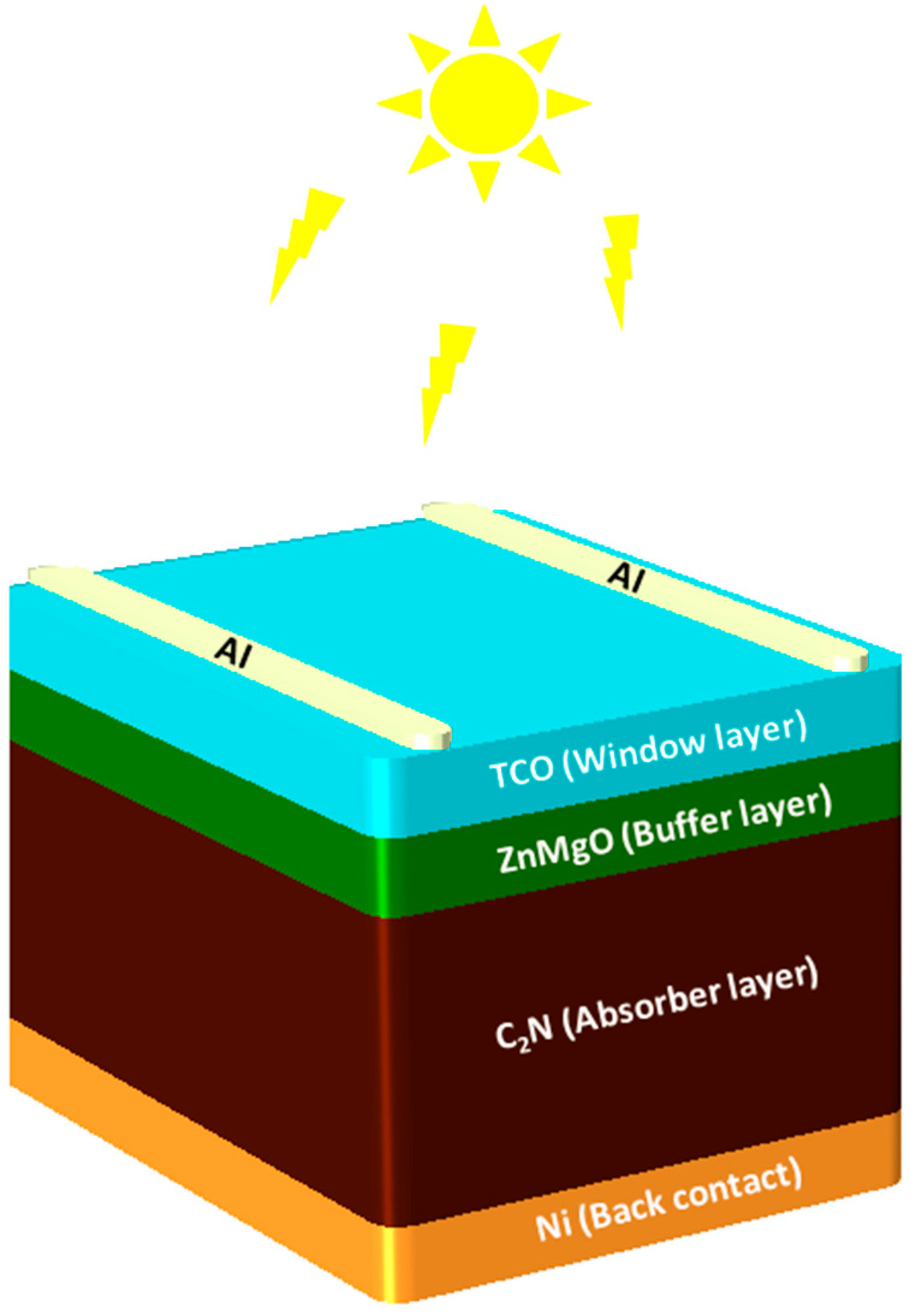
The basic architecture of the proposed C2N-based solar cell structure (Al/TCO/Zn1-xMgxO/C2N)/Ni) is shown in Figure 2. Simulations were conducted via the one-dimensional solar cell capacitance simulator SCAPS-1D (version 3.3.10). The SCAPS-1D was developed by Marc Burgelman and his colleague at the University of Gent, Belgium [28]. This software solves three basic equations for semiconductor devices, namely the Poisson equation and continuity equations for electrons and holes, as shown in Equations (1)–(3) [29,30], respectively.
Poisson   equation :   x ε o ε r Ψ x = q p n + N D + + N A + ρ q
Continuity   equation   for   electrons : 1 q J n x u n + G = n t
Continuity   equation   for   holes : 1 q J p x u p + G = p t
where Ψ is the wave function for electrostatic potential, and εo and εr are the permittivity of free space and the relative permittivity, respectively. The density of the defect charge is denoted by ρ, symbols n and p represent the free carrier concentrations for electrons and holes, the generation rate is denoted by G, and the ionized donor and acceptor densities are labelled as N D + and N A , respectively. In addition, Jn and Jp represent the current densities of the electron and hole, respectively. The SCAPS-1D is capable of performing in a variety of conditions, such as light and dark, different device operating temperatures and rear-contact voltages, and integrating various interfaces states. The program solves the above semiconductor equations by using input parameters that are appropriate for the working conditions and generating output parameters that represent the solar cell performance. This research focus on the investigation of key performance parameters represented by open-circuit voltage (Voc), short-circuit current density (Jsc), fill factor (FF), and power conversion efficiency (PCE) to evaluate the performance of the solar cell.
The solar cell input parameters depend on the accuracy of the results generated by the simulator. Therefore, the material parameters for each layer are selected carefully from authentic literature, as summarized in Table 1 [18,19,31,32,33]. The simulation parameters for interfacial defects are presented in Table 2, while the metal contact electrodes and operating temperatures are listed in Table 3. In the first stage of optimization, at a defect density of 1014 cm−3, the C2N layer thickness was changed from 50 nm to 1000 nm while keeping the acceptor density, thickness, and donor density of C2N and ZMO constant at 1015 cm−3, 30 nm, and 1015 cm−3, respectively. At the optimum thickness of C2N, the acceptor concentration was changed from 1013 cm−3 to 1018 cm−3. In the second stage, the buffer layers were optimized following the same procedure. Finally, the optimized cells are examined at different levels of bulk and interface defects, and their stability is studied by changing the operating temperature.

3. Results and Discussion

3.1. Energy Band Alignment

The band alignment of semiconductor materials is crucial in determining solar cells’ performance. When two dissimilar semiconductor materials combine in a heterojunction structure, a discontinuity in the conduction band (CB) forms. These misalignments are represented as the conduction band offset (CBO). The values of the CBO at the interface of the absorber layer and the buffer layer are listed in Table 4, and are calculated using the following equation:
CBO = χ C 2 N χ ZMO
Generally, the band offset is of two types: (i) cliff and (ii) spike. Cliff (negative CBO) will be generated if the CB level of the C2N layer is above the CB of the ZMO; otherwise, spike (positive CBO) will be formed, as illustrated in Figure 3a–d. The cliff offset reduces the built-in potential of the cell, while the spike offset increases it. In a C2N/ZMO heterostructure, as the Mg concentration increases from x = 0.0625 to x = 0.1875, the band gap of Zn1−xMgxO increases, which improves the energy band alignment and enhances the solar cell performance. Whereas at x = 0.25, the increase in band gap causes a large CBO, which reduces the efficiency. The interface between the C2N and ZMO (0.0625) forms a small cliff (negative CBO) of −0.02 eV. Although cliff does not hinder the flow of charge carriers from the absorber to the buffer layer, it decreases the built-in potential, which subsequently reduces the charge carriers’ separation at the interface. A minute spike (CBO of 0.05 eV) at the C2N/ZMO (x = 0.125) interface causes an increase in the built-in potential, which increases the flow of electrons and improves the cell’s performance as compared to the first structure. A moderate spike (CBO of 0.21 eV) at the C2N/ZMO (x = 0.1875) further enhances the built-in potential at the heterojunction, which hinders the photogenerated charge carriers from going back to the junction interface and suppresses charge recombination, hence improving the device performance. Moreover, a large spike at the interface between C2N and ZMO (x = 0.25) creates a large built-in potential; it also significantly hinders the electrons from flowing through the junction. Thus additional drift fields are needed to ensure the flow of electrons through the junction, consequently degrading the solar cell performance.
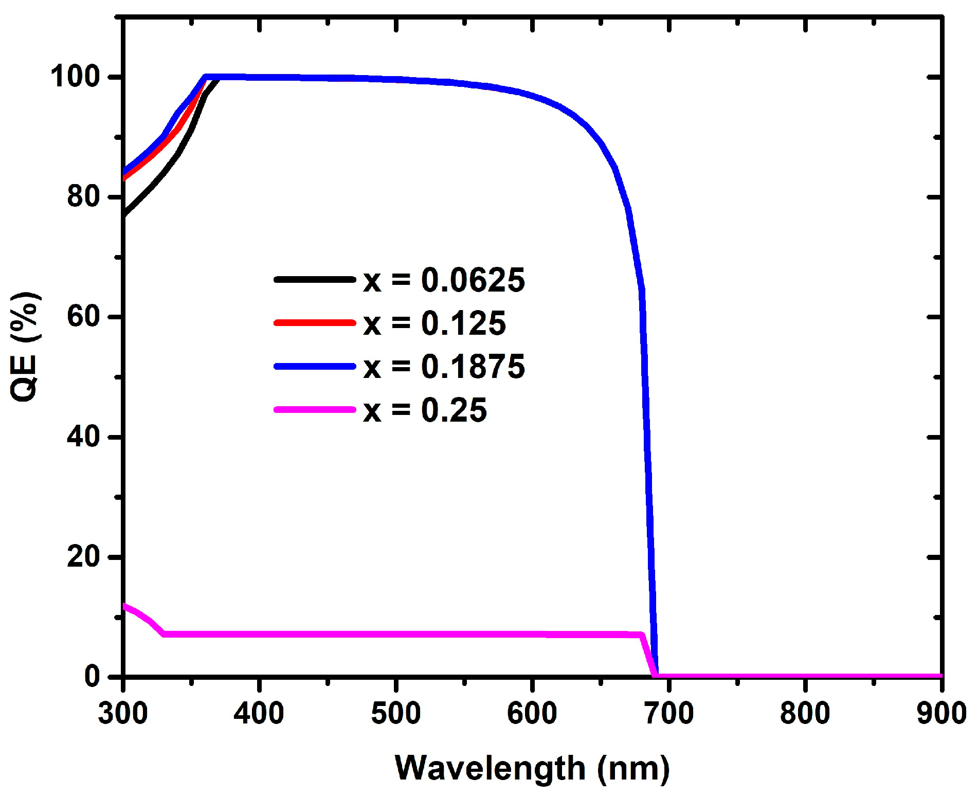
Furthermore, the absorption behavior of the investigated buffer layers indicates that the QE improves as the Mg doping of the ZMO layer increases from x = 0.0625 to x = 0.1875, as shown in Figure 4. Below 700 nm, the QE response to the incident light spectrum displays a noticeable variation for various buffer layers. On the other hand, when the Mg concentration increases to x = 0.25 a CBO of 0.39 eV is formed which produces a large spike at the heterojunction of the two layers. This large spike causes huge hurdles in the movement of electrons from the absorber to the buffer layer, which in turn increases recombination. The increase in the recombination rate reduces the amount of photogenerated charge carriers collected at the back electrode of the solar cell, which drastically affects the QE and reduces it.
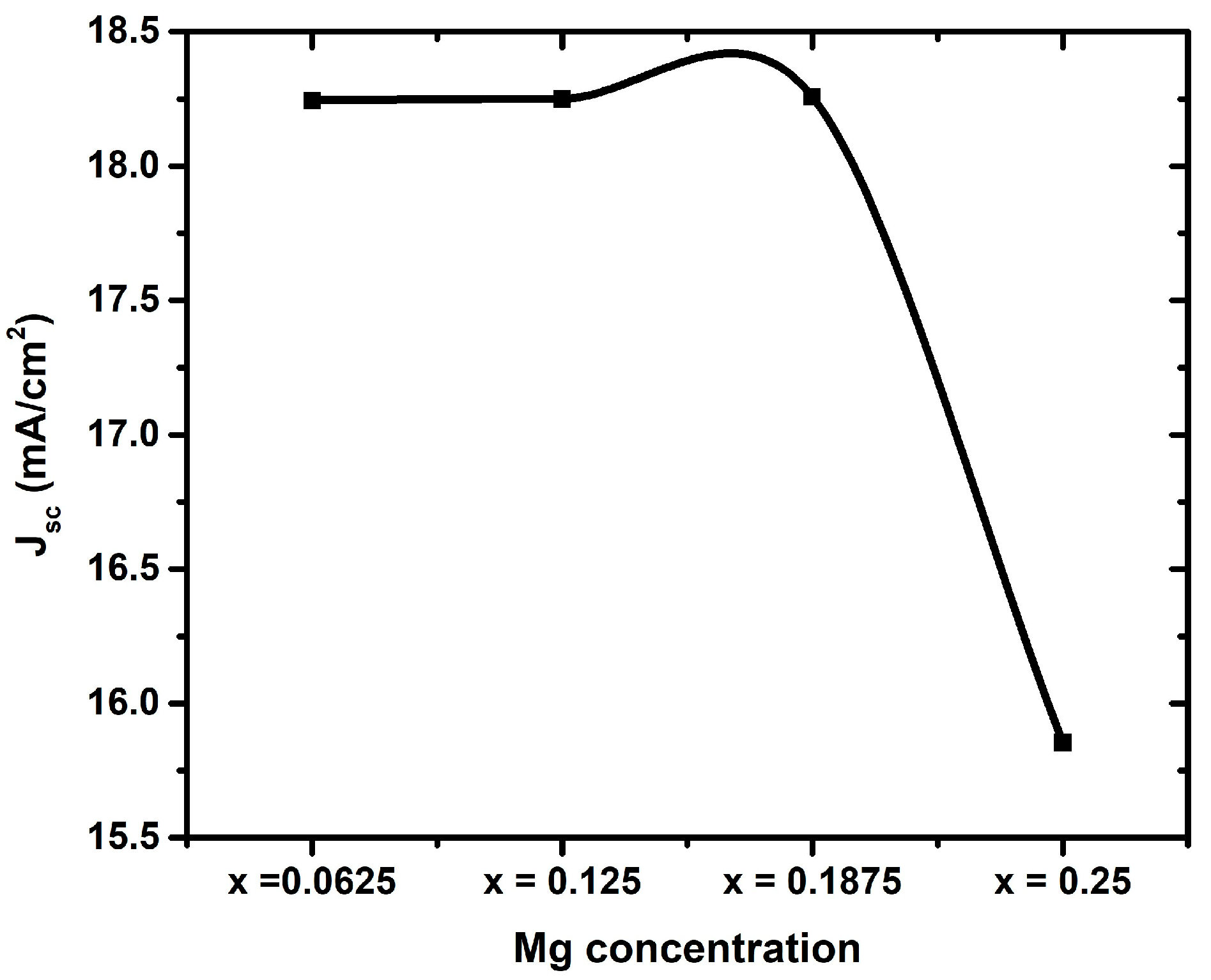
Therefore, the energy band alignment of C2N/ZMO structures demonstrates that a spike (positive CBO) interface helps in improving cell performance. However, a large spike (overly positive CBO) creates a barrier for the photogenerated charge carriers, lowering the short circuit current (Jsc) Figure 5 and efficiency.

3.2. Thickness Optimization of the C2N Layer

The absorber layer thickness significantly influences the overall device efficiency [9,18,35]. In solar cells, an absorber layer with a thickness of a few hundred nanometers is sufficient for efficient photocurrent generation. We performed our simulations by varying the absorber layer thickness from 50 nm to 1000 nm. For a C2N/ZMO (x = 0.1875) structure, the essential PV parameters, Voc, Jsc, and PCE, improved, as shown in Figure 6a,b,d. Above a thickness of 500 nm, the photogenerated charge carriers increased; however, as we increased the thickness to a maximum of 1000 nm, a partial recombination of the charge carriers occurred in the C2N layer, causing saturation in the performance. On the other hand, the fill factor (FF) demonstrates unusual variation when increasing the thickness of the C2N layer, as shown in Figure 6c. It starts with a downtrend but gradually increases from a 700 nm thickness. Similar behavior was observed in the previously reported literature on C2N and perovskite [9,19]. It can be ascribed to the charge carriers’ diffusion length, which changes the series resistance and decreases the internal power. From 50 nm to 700 nm, the absorber layer thickness is larger than the diffusion length, hence recombination takes place, which causes the series resistance to increase and the internal power to deplete, leading to a drop in FF. Above 700 nm, the absorption increases as the diffusion length exceeds the absorber layer thickness, and the FF rises again.
In addition, the positive impact of the absorber layer on solar cell performance in terms of quantum efficiency (QE) and short circuit current (Jsc) can be seen in Figure 6e,f, where increasing C2N thickness improves the absorption process and increases electron-hole pairs generation. Thus, the optimum device performance was obtained at a thickness of 1000 nm with the following parameters: PCE of 18.61 %, Voc of 1.23 V, Jsc of 18.25 mA/cm2, and FF of 83.16 %.

3.3. Impact of C2N Defect Density

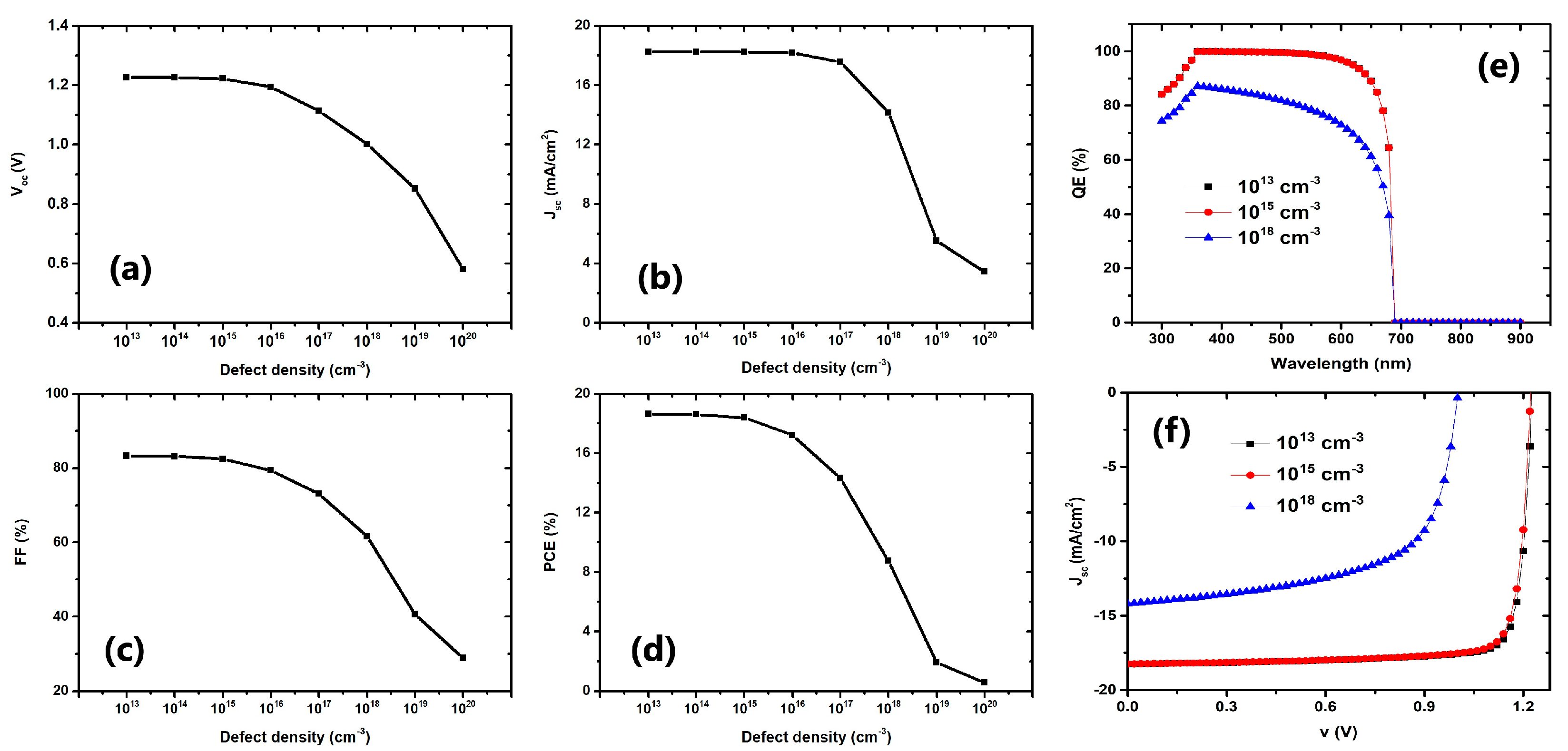
As a member of the graphene family, C2N may contain defect points, such as vacancies, interstitial atoms, and impurities [36]. Some deep defect points in C2N could contribute to optical absorption and reduce the band gaps, while others negatively impact the C2N band structure [37]. The presence of deep defect points in the absorber layer may trap the photogenerated charge carriers and block them from reaching the back contact, thereby reducing the device’s performance. Experimental studies have found graphene-like materials to have defect densities varying from 1010 cm−3 to 1014 cm−3 [38,39]. Moreover, several articles in the literature reported on the impact of defect density in SCAPS-simulation ranges from 1013 cm−3 to 1020 cm−3 [40,41]. In this study, the C2N layer is examined at three defect levels: low, average, and deep, from 1013 cm−3 to 1020 cm−3. According to the simulated results, the solar cell parameters sharply decrease by increasing the defect density above 1015 cm−3, as illustrated in Figure 7a–d. The sharp decrease in Voc and Jsc with increasing defect density is ascribed to high series resistance and poor fill factor [18].
Furthermore, the bandgap tuning is caused by the increase in defect density which deteriorates the light absorption process [19], thereby adversely impacting the quantum efficiency (QE) and the current-voltage curve (J-V) of the cell, as can be seen from Figure 7e,f. Although simulating solar cell devices at an extremely low defect density exhibits high performance, it is challenging to develop such devices experimentally [42]. Therefore, we performed our simulations at a defect density of 1014 cm−3 with a recorded PCE of 18.61%.

3.4. Influence of C2N-Doping Density

Numerous studies have indicated that doping in the absorber layer improves the overall performance of the solar cell [18,19,43,44]. However, doping above a certain level could enable the structure to develop a depletion region forced by an internal voltage and deteriorate the cell’s performance [43]. Such a depletion region potentially traps free charge carriers and changes the electronic behavior of the material, consequently degrading the solar cell efficiency. We varied the acceptor doping level of C2N from 1 × 1013 cm−3 to 1 × 1018 cm−3. The variation in the solar cell performance parameters with an increase in the doping level is shown in Figure 8. The Voc increases exponentially as the doping value increases. Above 1015 cm−3, Jsc declines drastically due to the high recombination rate and the increase in the series resistance of the cell, resulting in poor performance. According to our simulations, the optimum acceptor density level for C2N is selected at 1015 cm−3, with an achieved PCE of 18.61%.

3.5. Thickness Optimization of the Buffer Layer

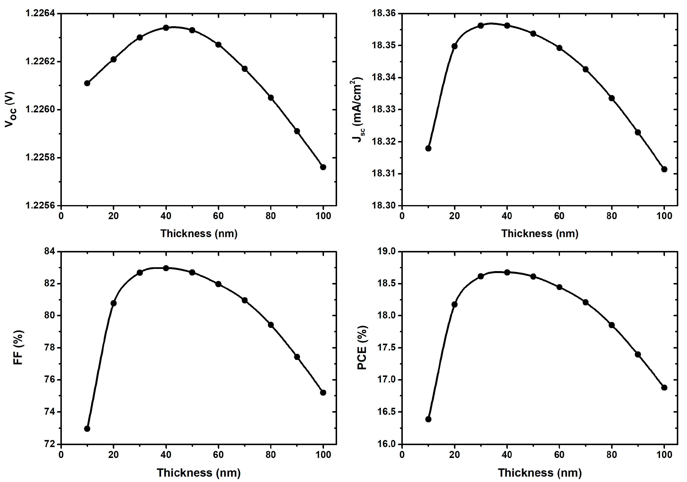
In a C2N/ZMO structure, incident light passes through the buffer layer into the absorber layer. Therefore, optimizing the buffer layer thickness is an essential step for improving the photogeneration process in the cell. In this study, the performance of C2N-based solar cells is investigated by varying the buffer layer thickness in the range of 10 nm to 100 nm while keeping the thickness of the absorber layer constant at 1000 nm. As shown in Figure 9, when the thickness of the ZMO (x = 0.1875) layer increases, the Voc, Jsc, FF, and PCE decline after reaching the maximum point. This behavior is due to the high absorption of photons in the buffer layer region. Therefore, fewer photons reach the junction, which limits the generation of electron-hole pairs. Generally, a very thin buffer layer allows a high level of photon transmittance. However, two factors primarily prevent reducing the buffer layer thickness, i.e., the Schottky barrier structure, due to which the device performance could reverse, and the fabrication limitation [19]. Therefore, the optimum device performance is obtained at a thickness of 40 nm with a PCE of 18.67 %.

3.6. Optimization of the Buffer Layer Doping Density

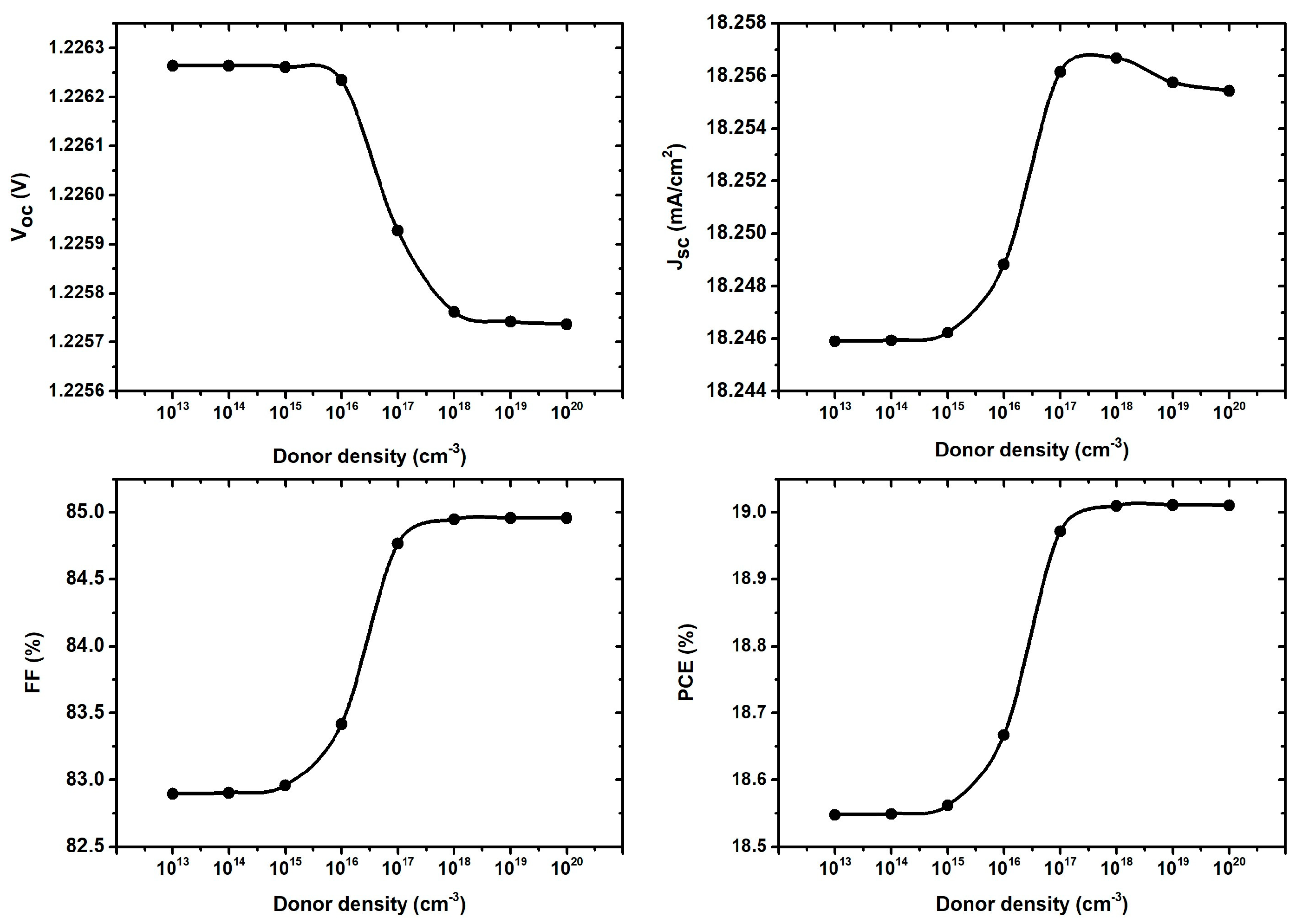
We investigated the cell performance by varying the doping concentration of ZMO from 1013 cm−3 to 1020 cm−3 while keeping the thickness of the absorber and the buffer layers constant at 1000 nm and 40 nm, respectively. The variation in the device performance parameters of the ZMO (x = 0.1875)-based structure is displayed in Figure 10, where the Voc sharply declines after 1016 cm−3. When the doping concentration increased from 1015 cm−3 to 1018 cm−3, the Jsc, FF, and PCE improved. According to the Moss–Burstein effect, semiconductor bandgaps can slightly increase with high doping, providing sufficient charge carriers and increasing conductivity [44]. The optimum recorded PCE of 19.01% is found at a donor concentration of 1018 cm−3.
The simulation results for C2N-based solar cells revealed that the performance parameters improved with a buffer layer Mg concentration from x = 0.0625 to x = 0.1875, as summarized in Table 5. Among the investigated structures, the C2N/ZMO (x = 0.25) acquires the lowest PCE of 17.71%, while the C2N/ZMO (x = 0.1875) yields the highest PCE of 19.01%. This value is higher than previously reported CdS and IGZO-containing C2N-based solar cells [18,19].

3.7. Effect of the Interface Defect of C2N/ZMO

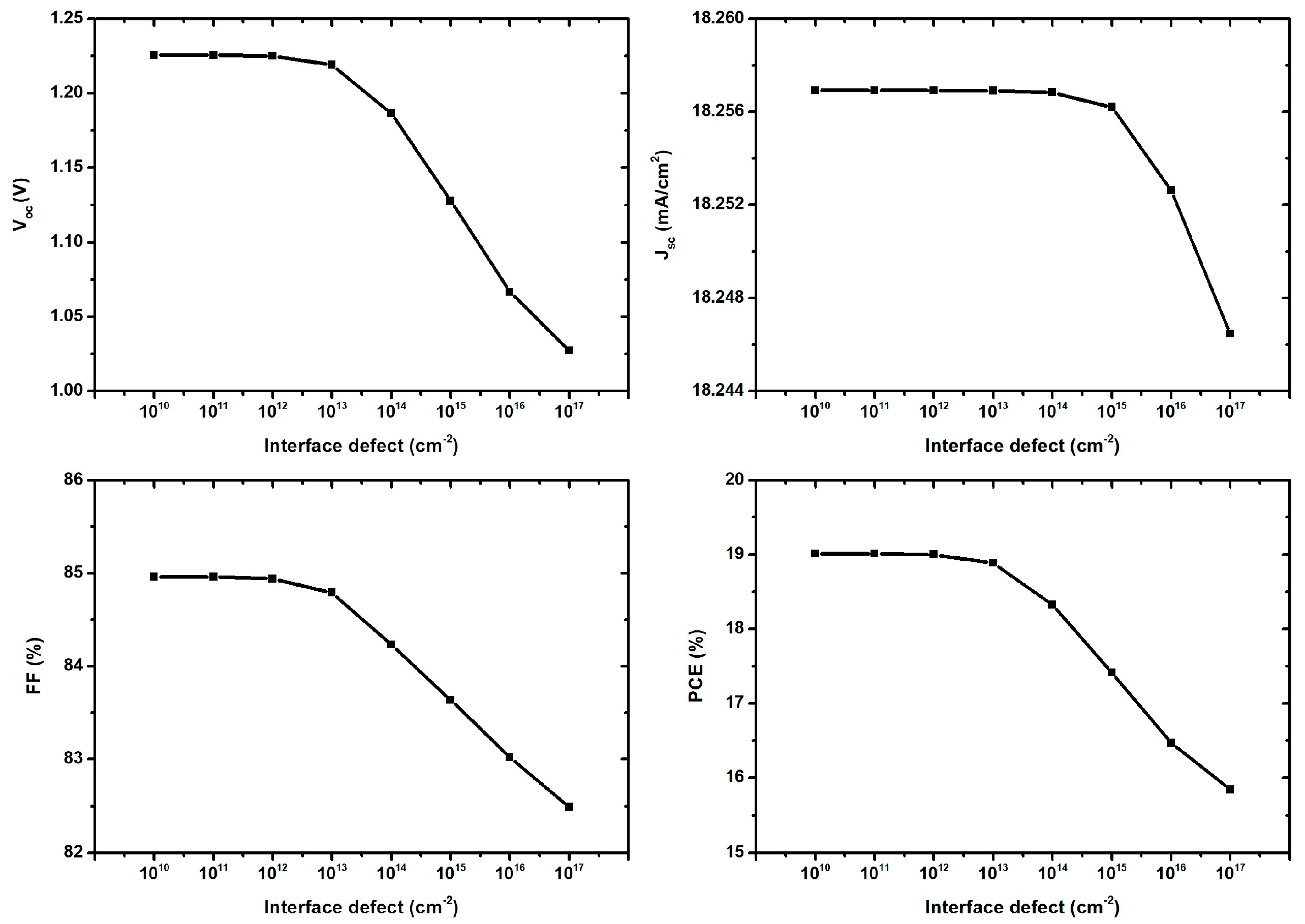
In solar cells, interface defects create recombination centers and traps, which prevent charge carriers from reaching the back contact. In this paper, the impact of interface defects on C2N-based solar cells is examined by changing their value from 1013 cm−2 to 1020 cm−2. As illustrated in Figure 11, the efficiency of an x = 0.1875-based structure decreased from 19.01% to 15.84% at 1013 cm−2 to 1020 cm−2, respectively. This drop in PCE is attributed to the Shockley––Read–Hall (SRH) recombination process, as shown in Equation (5) [45,46].
S R H = ϑ σ n σ p N T n p n i 2 σ p p p 1 + σ n n + n 1
where ϑ indicates the thermal velocity of an electron, and σn and σp represent the electrons and holes capture cross-sections, respectively. NT symbolizes the number of defects per unit volume, ni is the intrinsic number density, n and p denote the concentration of electrons and holes at equilibrium, and n1 and p1 are the concentrations of electrons and holes in the trap defect and valence band, respectively. According to Equation (5), it appears that increasing defects can cause trapping centers at the interface for charge carriers to recombine, resulting in the degradation of solar cell performance.

3.8. Impact of Temperature Variation on the Device Performance

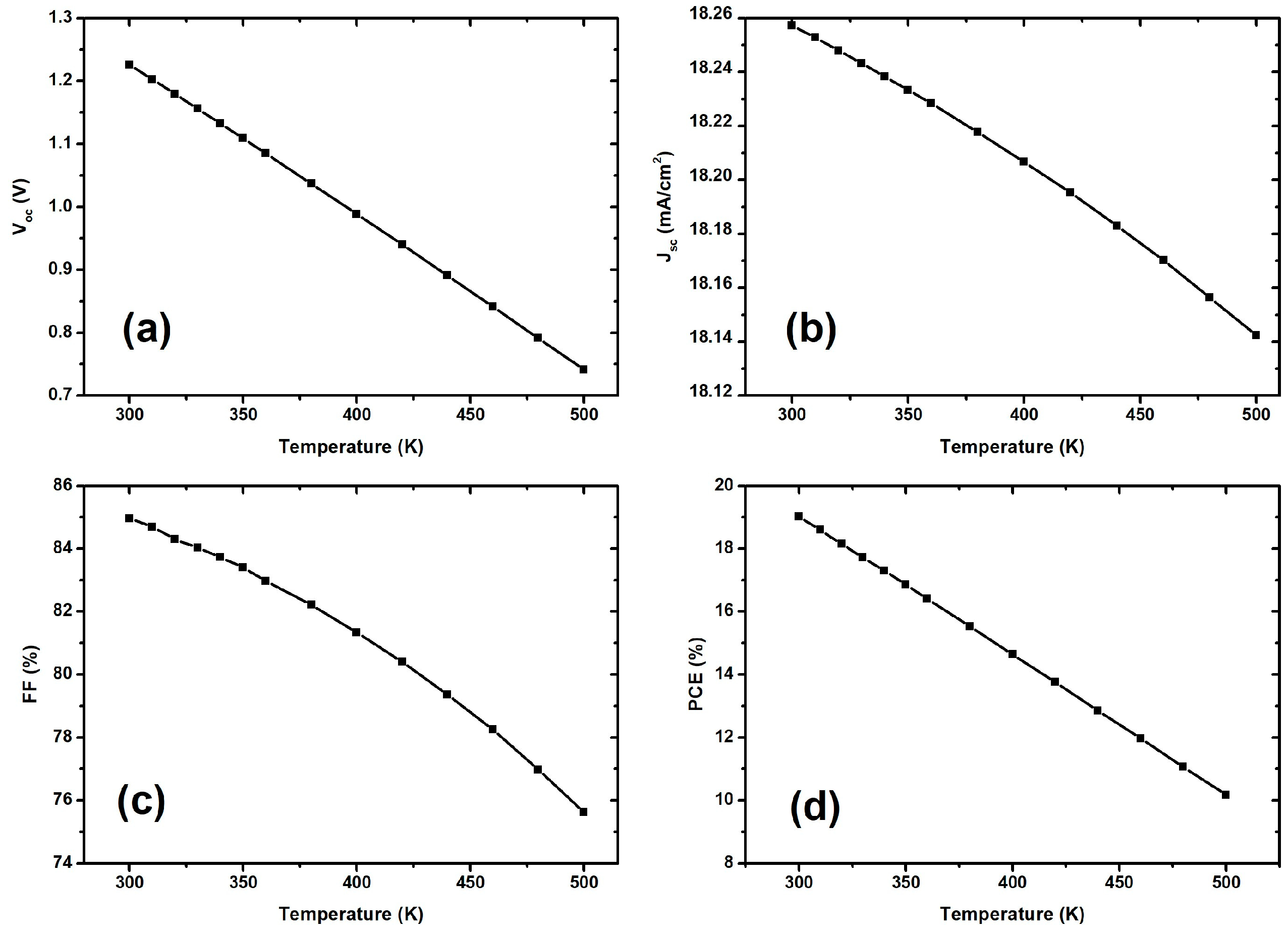
Solar cells are temperature-sensitive devices, thereby high operating temperatures significantly lower their overall performance [30,47,48,49]. In TFSc, the rise in operating temperature leads to an increase the recombination rate, which heats up the cell and deteriorates its overall performance [50]. We examined the stability of the C2N/ZMO (0.1875)-based cell by implementing an operating temperature in the range of 300 k to 500 k. The PV parameters, such as Voc, Jsc, FF, and PEC sharply decreased with the rise in temperature, as shown in Figure 12a–d. At the given temperatures, the efficiency decreased from 19.01% to 10.17% at 300 k and 500 k, respectively. All other structures (not shown) exhibited similar behavior. The sharp drop in performance parameters is attributed to the high operating temperatures, which deformed the cell’s layers, shortened the diffusion length, and caused a weak interlayer connection. As a result, increasing the recombination rate and series resistance hinders the flow of photogenerated charge carriers from reaching the back contact and degrades solar cell efficiency.

4. Conclusions

This study presents the detailed numerical simulations of C2N-based solar cells with the (AI/TCO/Zn1−xMgxO/C2N)/Ni) device structure using the SCAPS-1D software. The influence of four Mg content levels on the performance of the Zn1−xMgxO/C2N heterojunction has been investigated. The simulations revealed that increasing the Mg concentration beyond x = 0.1875 can deteriorate the solar cell performance. Among the investigated buffer layers, x = 0.1875 achieved the highest efficiency, whereas x = 0.25 performed the least well. The thickness of C2N was found to have a significant influence on the PV parameters, with an optimum selected thickness of 1000 nm. When the acceptor density of C2N was increased to 1 × 1015 cm−3, a stable performance was observed in the device. The same stability was found for the buffer layers when the thickness and doping density were set at 40 nm and 1 × 1018 cm−3, respectively. Additionally, the high defect density in the absorber layer and at the C2N/ZMO interface accelerated the recombination rate, which caused the degradation of solar efficiency. Furthermore, the temperature analysis showed that the solar cell is susceptible to high operating temperatures. The findings of this contribution highlight the potential for C2N-based heterojunction solar cells as an emerging thin-film PV technology.

Author Contributions

Conceptualization, W.A. and A.D.K.; methodology, W.A., W.F., M.J. and A.D.K.; software, W.A.; validation, J.P., R.G. and S.T.J.; formal analysis, J.P., Z.L. and R.G.; investigation, W.A.; resources, Z.L.; data curation, W.A., W.F. and A.D.K.; writing—original draft preparation, W.A.; writing—review and editing, W.A., W.F., A.D.K., S.T.J., R.G. and J.P.; visualization, J.P.; supervision, A.D.K. and M.J.; project administration, A.D.K.; funding acquisition, Z.L. All authors have read and agreed to the published version of the manuscript.

Funding

An SGS grant was received from VSB—Technical University of Ostrava under grant number SP2022/21.

Data Availability Statement

Data will be sent on request by the first author of the paper.

Acknowledgments

The authors are grateful to Marc Burgelman from the University of Gent, Belgium, for providing the SCAPS 1-D simulation software.

Conflicts of Interest

The authors declare no conflict of interest.

References

  1. Raha, S.; Pal, S. A Study on the Present Environmental Scenario due to Pollution by Conventional Energy Sources—And Remedies: Solar Cell with Nanotechnology. Strat. Plan. Energy Environ. 2010, 30, 8–19. [Google Scholar] [CrossRef]
  2. Suri, M.; Betak, J.; Rosina, K.; Chrkavy, D.; Suriova, N.; Cebecauer, T.; Caltik, M.; Erdelyi, B. Global Photovoltaic Power Potential by Country; ESMAP: Washington, DC, USA, 2020. [Google Scholar]
  3. Soley, S.S.; Dwivedi, A.D.D. Advances in high efficiency crystalline silicon homo junction solar cell technology. AIP Conf. Proc. 2019, 2104, 030033. [Google Scholar] [CrossRef]
  4. Kuddus, A.; Ismail, A.B.M.; Hossain, J. Design of a highly efficient CdTe-based dual-heterojunction solar cell with 44% predicted efficiency. Sol. Energy 2021, 221, 488–501. [Google Scholar] [CrossRef]
  5. Zhang, W.-W.; Qi, H.; Ji, Y.-K.; He, M.-J.; Ren, Y.-T.; Li, Y. Boosting photoelectric performance of thin film GaAs solar cell based on multi-objective optimization for solar energy utilization. Sol. Energy 2021, 230, 1122–1132. [Google Scholar] [CrossRef]
  6. Farooq, W.; Alshahrani, T.; Kazmi, S.A.A.; Iqbal, J.; Khan, H.A.; Khan, M.; Raja, A.A.; Rehman, A.U. Materials Optimization for thin-film copper indium gallium selenide (CIGS) solar cell based on distributed braggs reflector. Optik 2021, 227, 165987. [Google Scholar] [CrossRef]
  7. Bangash, K.; Kazmi, S.; Farooq, W.; Ayub, S.; Musarat, M.; Alaloul, W.; Javed, M.; Mosavi, A. Thickness Optimization of Thin-Film Tandem Organic Solar Cell. Micromachines 2021, 12, 518. [Google Scholar] [CrossRef]
  8. Gusain, A.; Faria, R.M.; Miranda, P.B. Polymer Solar Cells—Interfacial Processes Related to Performance Issues. Front. Chem. 2019, 7, 61. [Google Scholar] [CrossRef] [PubMed] [Green Version]
  9. Yasin, S.; Al Zoubi, T.; Moustafa, M. Design and simulation of high efficiency lead-free heterostructure perovskite solar cell using SCAPS-1D. Optik 2021, 229, 166258. [Google Scholar] [CrossRef]
  10. Sun, J.; Zhang, R.; Li, X.; Yang, J. A many-body GW+ BSE investigation of electronic and optical properties of C2N. Appl. Phys. Lett. 2016, 13, 133108. [Google Scholar] [CrossRef] [Green Version]
  11. Xu, J.; Mahmood, J.; Dou, Y.; Dou, S.; Li, F.; Dai, L.; Beak, J.B. 2D frameworks of C2N and C3N as new anode materials for lithium-ion batteries. Adv. Mater. 2017, 34, 1702007. [Google Scholar] [CrossRef]
  12. Tsoeu, S.E. First-Principles Design of Hybrid Carbon Nitride (C2n) with Gallium Sulphide and Gallium Selenide Two-Dimensional (2D) Materials as High-Performance Photovoltaic Cells; University of Johannesburg: Johannesburg, South Africa, 2021. [Google Scholar]
  13. Mak, K.F.; Lee, C.; Hone, J.; Shan, J.; Heinz, T.F. Atomically thin MoS2: A new direct-gap semiconductor. Phys. Rev. Lett. 2010, 13, 136805. [Google Scholar] [CrossRef] [PubMed] [Green Version]
  14. Roy, S.; Bermel, P. Electronic and optical properties of ultra-thin 2D tungsten disulfide for photovoltaic applications. Sol. Energy Mater. Sol. Cells 2018, 174, 370–379. [Google Scholar] [CrossRef]
  15. Tiwari, S.K.; Sahoo, S.; Wang, N.; Huczko, A. Graphene research and their outputs: Status and prospect. J. Sci. Adv. Mater. Devices 2020, 5, 10–29. [Google Scholar] [CrossRef]
  16. Mahmood, J.; Lee, E.K.; Jung, M.; Shin, D.; Jeon, I.-Y.; Jung, S.-M.; Choi, H.-J.; Seo, J.-M.; Bae, S.-Y.; Sohn, S.-D.; et al. Nitrogenated holey two-dimensional structures. Nat. Commun. 2015, 6, 6486. [Google Scholar] [CrossRef] [Green Version]
  17. Sahin, H. Structural and phononic characteristics of nitrogenated holey graphene. Phys. Rev. B 2015, 92, 085421. [Google Scholar] [CrossRef] [Green Version]
  18. Zhou, X.; Han, J. Design and simulation of C2N based solar cell by SCAPS-1D software. Mater. Res. Express 2020, 7, 126303. [Google Scholar] [CrossRef]
  19. Yasin, S.; Abu Waar, Z.; Al Zoubi, T.; Moustafa, M. Optoelectronic simulation of a high efficiency C2N based solar cell via buffer layer optimization. Opt. Mater. 2021, 119, 111364. [Google Scholar] [CrossRef]
  20. Minemoto, T.; Murata, M. Theoretical analysis on effect of band offsets in perovskite solar cells. Sol. Energy Mater. Sol. Cells 2015, 133, 8–14. [Google Scholar] [CrossRef]
  21. Peelaers, H.; Kioupakis, E.; Van de Walle, C.G. Fundamental limits on optical transparency of transparent conducting oxides: Free-carrier absorption in SnO. Appl. Phys. Lett. 2012, 100, 011914. [Google Scholar] [CrossRef] [Green Version]
  22. Kephart, J.; McCamy, J.; Ma, Z.; Ganjoo, A.; Alamgir, F.; Sampath, W. Band alignment of front contact layers for high-efficiency CdTe solar cells. Sol. Energy Mater. Sol. Cells 2016, 157, 266–275. [Google Scholar] [CrossRef]
  23. Ke, Y.; Lany, S.; Berry, J.J.; Perkins, J.D.; Parilla, P.A.; Zakutayev, A.; Ohno, T.; O’Hayre, R.; Ginley, D.S. Enhanced Electron Mobility Due to Dopant-Defect Pairing in Conductive ZnMgO. Adv. Funct. Mater. 2014, 24, 2875–2882. [Google Scholar] [CrossRef]
  24. Bahfir, A.; Boumaour, M.; Kechouane, M. Prospects of potential ZnMgO front layer in CZTS solar cells. Optik 2018, 169, 196–202. [Google Scholar] [CrossRef]
  25. Ren, S.; Wang, H.; Li, Y.; Li, H.; He, R.; Wu, L.; Li, W.; Zhang, J.; Wang, W.; Feng, L. Rapid thermal annealing on ZnMgO window layer for improved performance of CdTe solar cells. Sol. Energy Mater. Sol. Cells 2018, 187, 97–103. [Google Scholar] [CrossRef]
  26. Ren, S.; Li, H.; Lei, C.; Li, C.; Yin, X.; Wu, L.; Li, W.; Zhang, J.; Wang, W.; Feng, L. Interface modification to enhance electron extraction by deposition of a ZnMgO buffer on SnO2-coated FTO in CdTe solar cells. Sol. Energy 2018, 177, 545–552. [Google Scholar] [CrossRef]
  27. Mohammadnejad, S.; Bahnamiri, Z.M.; Maklavani, S.E. Enhancement of the performance of kesterite thin-film solar cells using dual absorber and ZnMgO buffer layers. Superlattices Microstruct. 2020, 144, 106587. [Google Scholar] [CrossRef]
  28. Burgelman, M.M. Simulation Programme SCAPS-1D for Thin Film Solar Cells Developed at ELIS, University of Gent. Available online: https://scaps.elis.ugent.be/ (accessed on 2 February 2022).
  29. Anwar, F.; Mahbub, R.; Satter, S.S.; Ullah, S.M. Effect of Different HTM Layers and Electrical Parameters on ZnO Nanorod-Based Lead-Free Perovskite Solar Cell for High-Efficiency Performance. Int. J. Photoenergy 2017, 2017, 9846310. [Google Scholar] [CrossRef]
  30. Adewoyin, A.D.; Olopade, M.A.; Oyebola, O.O.; Chendo, M.A. Development of CZTGS/CZTS tandem thin film solar cell using SCAPS-1D. Optik 2018, 176, 132–142. [Google Scholar] [CrossRef]
  31. He, X.; Wu, L.; Hao, X.; Zhang, J.; Li, C.; Wang, W.; Feng, L.; Du, Z. The Band Structures of Zn1−xMgxO (In) and the simulation of CdTe solar cells with a Zn1−xMgxO (In) window layer by SCAPS. Energies 2019, 2, 291. [Google Scholar] [CrossRef] [Green Version]
  32. Gamal, N.; Sedky, S.H.; Shaker, A.; Fedawy, M. Design of lead-free perovskite solar cell using Zn1−xMgxO as ETL: SCAPS device simulation. Optik 2021, 242, 167306. [Google Scholar] [CrossRef]
  33. He, X.; Song, Y.; Wu, L.; Li, C.; Zhang, J.; Feng, L. Simulation of high-efficiency CdTe solar cells with Zn1−xMgxO window layer by SCAPS software. Mater. Res. Express 2018, 6, 065907. [Google Scholar] [CrossRef]
  34. Michaelson, H.B. The work function of the elements and its periodicity. J. Appl. Phys. 1977, 48, 4729–4733. [Google Scholar] [CrossRef] [Green Version]
  35. Fox, M. Optical Properties of Solids; Oxford University Press: New York, NY, USA, 2010. [Google Scholar]
  36. Araujo, P.T.; Terrones, M.; Dresselhaus, M.S. Defects and impurities in graphene-like materials. Mater. Today 2012, 15, 98–109. [Google Scholar] [CrossRef] [Green Version]
  37. Zhang, H.; Zhang, X.; Yang, G.; Zhou, X. Point Defect Effects on Photoelectronic Properties of the Potential Metal-Free C2N Photocatalysts: Insight from First-Principles Computations. J. Phys. Chem. 2018, 122, 5291–5302. [Google Scholar] [CrossRef]
  38. Zhong, J.-H.; Zhang, J.; Jin, X.; Liu, J.-Y.; Li, Q.; Li, M.-H.; Cai, W.; Wu, D.-Y.; Zhan, D.; Ren, B. Quantitative Correlation between Defect Density and Heterogeneous Electron Transfer Rate of Single Layer Graphene. J. Am. Chem. Soc. 2014, 136, 16609–16617. [Google Scholar] [CrossRef] [PubMed]
  39. Gawlik, G.; Ciepielewski, P.; Baranowski, J.M. Study of Implantation Defects in CVD Graphene by Optical and Electrical Methods. Appl. Sci. 2019, 9, 544. [Google Scholar] [CrossRef] [Green Version]
  40. Haider, S.Z.; Anwar, H.; Wang, M. A comprehensive device modelling of perovskite solar cell with inorganic copper iodide as hole transport material. Semicond. Sci. Technol. 2018, 33, 035001. [Google Scholar] [CrossRef] [Green Version]
  41. Ouslimane, T.; Et-Taya, L.; Elmaimouni, L.; Benami, A. Impact of absorber layer thickness, defect density, and operating temperature on the performance of MAPbI3 solar cells based on ZnO electron transporting material. Heliyon 2021, 7, e06379. [Google Scholar] [CrossRef] [PubMed]
  42. Gan, Y.; Bi, X.; Liu, Y.; Qin, B.; Li, Q.; Jiang, Q.; Mo, P. Numerical Investigation Energy Conversion Performance of Tin-Based Perovskite Solar Cells Using Cell Capacitance Simulator. Energies 2020, 13, 5907. [Google Scholar] [CrossRef]
  43. Sarilmaz, A.; Ozel, F.; Aljabour, A.; Khaskheli, A.R.; Kus, M. Effect of doping on thin film solar cell efficiency based on ZnMn2O4 nanocrystals. Mater. Today Proc. 2019, 18, 1861–1867. [Google Scholar] [CrossRef]
  44. Trukhanov, V.A.; Bruevich, V.V.; Paraschuk, D. Effect of doping on performance of organic solar cells. Phys. Rev. B 2011, 84, 205318. [Google Scholar] [CrossRef]
  45. Chowdhury, M.; Shahahmadi, S.; Chelvanathan, P.; Tiong, S.; Amin, N.; Techato, K.; Nuthammachot, N.; Chowdhury, T.; Suklueng, M. Effect of deep-level defect density of the absorber layer and n/i interface in perovskite solar cells by SCAPS-1D. Results Phys. 2020, 16, 102839. [Google Scholar] [CrossRef]
  46. Shockley, W.; Read, W., Jr. Statistics of the recombinations of holes and electrons. Phys. Rev. 1952, 5, 835. [Google Scholar] [CrossRef]
  47. Mandadapu, U.; Vedanayakam, S.V.; Thyagarajan, K.; Babu, B. Optimisation of high efficiency tin halide perovskite solar cells using SCAPS-1D. Int. J. Simul. Process Model. 2018, 3, 221–227. [Google Scholar] [CrossRef]
  48. Alzoubi, T.; Moustafa, M. Numerical optimization of absorber and CdS buffer layers in CIGS solar cells using SCAPS. Int. J. Smart Grid Clean Energy 2019, 8, 291–298. [Google Scholar] [CrossRef]
  49. Jhuma, F.A.; Shaily, M.Z.; Rashid, M.J. Towards high-efficiency CZTS solar cell through buffer layer optimization. Mater. Renew. Sustain. Energy 2019, 8, 6. [Google Scholar] [CrossRef] [Green Version]
  50. Zandi, S.; Seresht, M.J.; Khan, A.; Gorji, N.E. Simulation of heat loss in Cu2ZnSn4SxSe4−x thin film solar cells: A coupled optical-electrical-thermal modeling. Renew. Energy 2022, 181, 320–328. [Google Scholar] [CrossRef]
Figure 1. Comparison of the crystal structures of (a) graphene (b) C2N-h2D. Adapted and modified from [16].
Processes 11 00091 g001
Figure 2. Schematic view of a C2N-based solar cell.
Processes 11 00091 g002
Figure 3. (ad) Energy band alignment at the C2N/ZMO interfaces.
Processes 11 00091 g003
Figure 4. Quantum efficiency (QE) behavior of the buffer layers under the light spectrum.
Processes 11 00091 g004
Figure 5. Variation in the short circuit current (Jsc) by increasing the Mg concentration in Zn1−xMgxO.
Processes 11 00091 g005
Figure 6. (ad) Influence of varying C2N thickness on PV parameters. (e,f) QE and J-V behavior with varied C2N thickness.
Processes 11 00091 g006
Figure 7. (ad) Variation in the PV parameters of C2N with defect density. (e,f) QE and current-voltage curve (J-V) behavior with varied C2N-defect density.
Processes 11 00091 g007
Figure 8. Variation in PV parameters by varying the C2N doping concentration.
Processes 11 00091 g008
Figure 9. Solar cell performance parameters with varying ZMO thickness.
Processes 11 00091 g009
Figure 10. Variation in the PV parameters by increasing the buffer layer doping density.
Processes 11 00091 g010
Figure 11. Variation in PV parameters for different defects at the C2N/ZMO interface.
Processes 11 00091 g011
Figure 12. Impact of temperature on C2N-based solar cell performance.
Processes 11 00091 g012
Table 1. Initial key input parameters for the SCAPS-1D simulation.
ParametersTCO
[19,32]
Zn1−xMgxO
[31,32,33]
C2N
[18,19]
x = 0.0625x = 0.125x = 0.1875x = 0.25
Thickness (nm)3030303030300
Band gap (eV)3.53.413.483.653.821.8
Electron affinity (eV)44.444.374.214.034.42
Dielectric Permittivity999994.5
CB-effective density of states (cm−3)2.2 × 10181 × 10179 × 10161 × 10161 × 10151 × 1019
VB-effective density of states (cm−3)1.8 × 10191 × 10189 × 10171 × 10171 × 10161 × 1015
Electron thermal velocity (cm/s)1 × 1071 × 1071 × 1071 × 1071 × 1071 × 107
Hole thermal velocity (cm/s)1 × 1071 × 1071 × 1071 × 1071 × 1071 × 107
Electron mobility
(cm2/(V·s))
205050505013
Hole mobility (cm2/(V·s))102020202020.6
Donor doping concentration (cm−3)1 × 10141 × 10141 × 10141 × 10141 × 10140
Acceptor doping concentration (cm−3)000001 × 1014
Defect density Nt (cm−3)1 × 10141 × 10141 × 10141 × 10141 × 10141 × 1014
Defect typeNeutralNeutralNeutralNeutralNeutralNeutral
Defect distributionSingleSingleSingleSingleSingleGaussian
Table 2. Interface layer settings for the SCAPS simulation.
ParametersTCO/ZMOZMO/C2N
Defect typeNeutralNeutral
Capture cross section of electrons (cm2)1 × 10−191 × 10−19
Capture cross section of holes (cm2)1 × 10−191 × 10−19
Energetic distributionSingleSingle
Energy level with respect to Ev (eV)0.60.6
Major carrier barrier height relative to Ef (eV)SCAPSSCAPS
Major carrier barrier height relative to Ev (eV)SCAPSSCAPS
Table 3. Input parameters used for front and back contacts in the simulation.
ParametersBack-Contact Metal ElectrodeFront-Contact Metal Electrode
Surface recombination velocity of electrons (cms−1)105107
Surface recombination velocity of holes (cms−1)107105
Work function (eV)5.35 Ni (111) [34]4.06 (AI) [34]
Working temperature (K)300
Table 4. CBO of C2N/ZMO heterostructures.
Buffer LayerCBO (eV)
C2N/Zn1−xMgxO (x = 0.0625)−0.02
C2N/Zn1−xMgxO (x = 0.125)0.05
C2N/Zn1−xMgxO (x = 0.1875)0.21
C2N/Zn1−xMgxO (x = 0.25)0.39
Table 5. C2N/ZMO-based solar cell parameters after optimization.
Simulated ParametersZn1−xMgxO
x = 0.0652x = 0.125x = 0.1875x = 0.25
Voc (V) 1.231.231.23 1.21
Jsc (mA/cm2) 18.24 18.2518.2618.23
FF (%) 84.8984.9484.9679.25
PCE (%) 18.981919.01 17.71
Disclaimer/Publisher’s Note: The statements, opinions and data contained in all publications are solely those of the individual author(s) and contributor(s) and not of MDPI and/or the editor(s). MDPI and/or the editor(s) disclaim responsibility for any injury to people or property resulting from any ideas, methods, instructions or products referred to in the content.