
Leveraging Dion–Jacobson Interface Hierarchies for Defect Alleviation in High-Efficiency and Durable Perovskite Solar Cells

Abstract
:
1. Introduction
2. Results
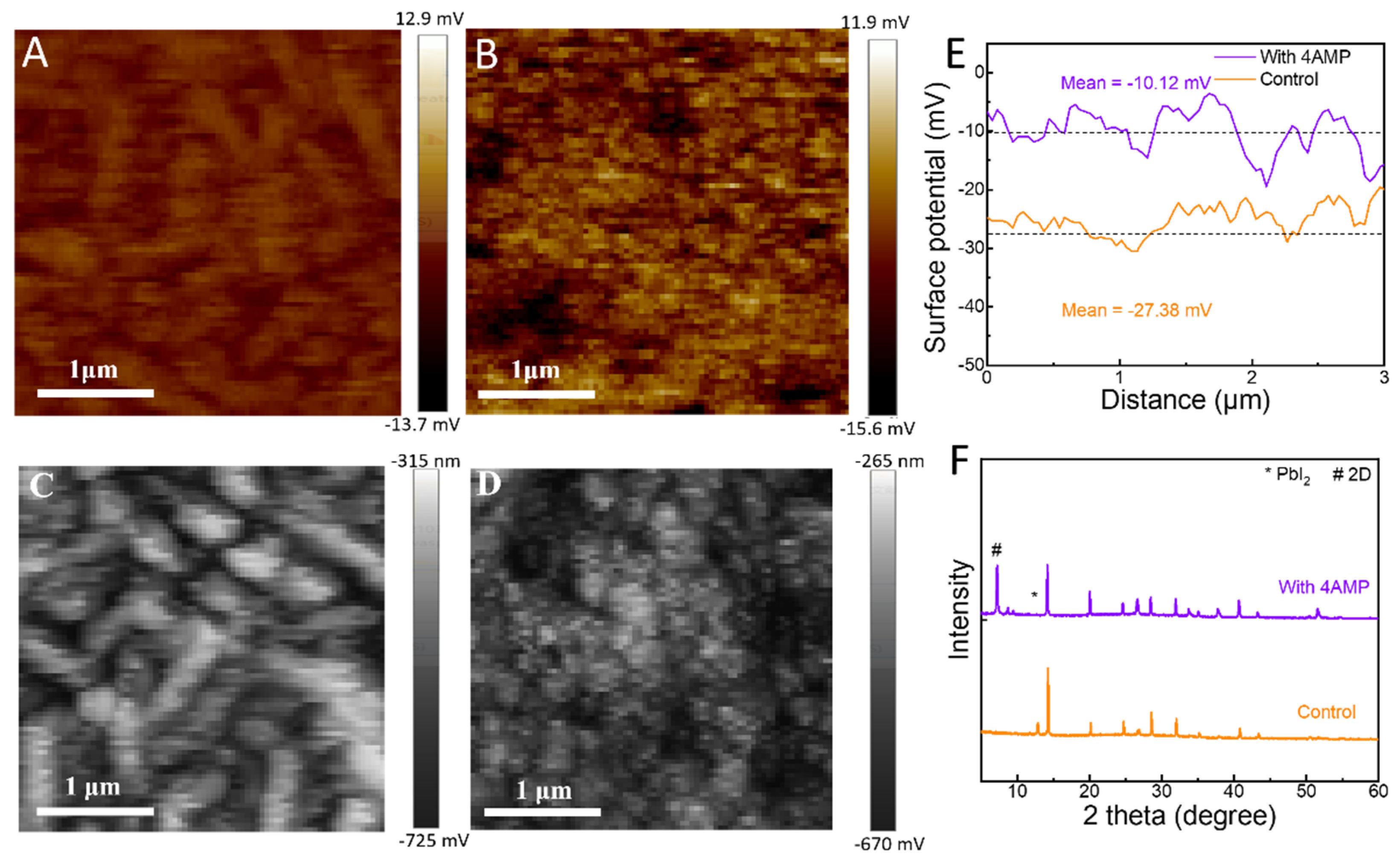
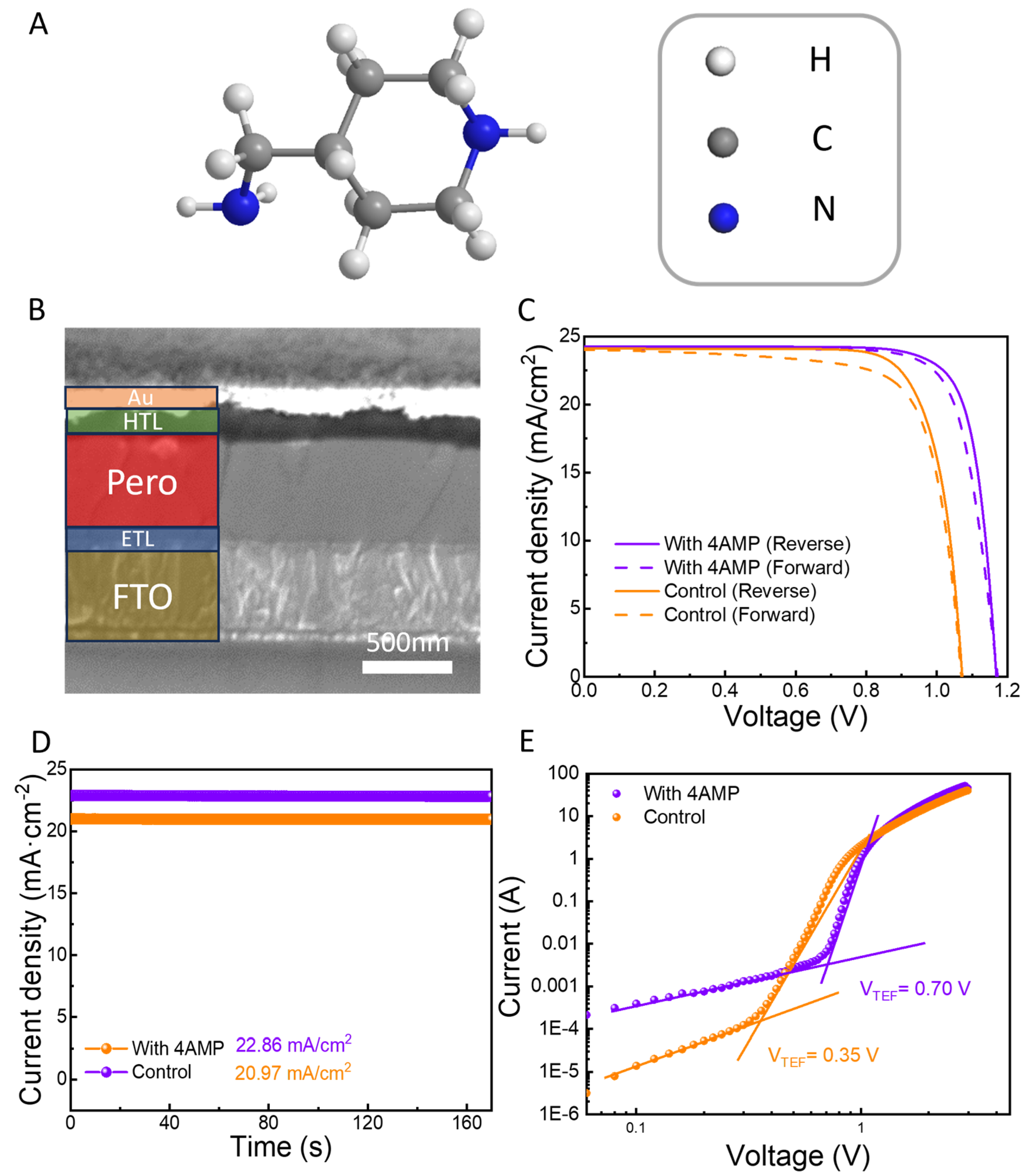
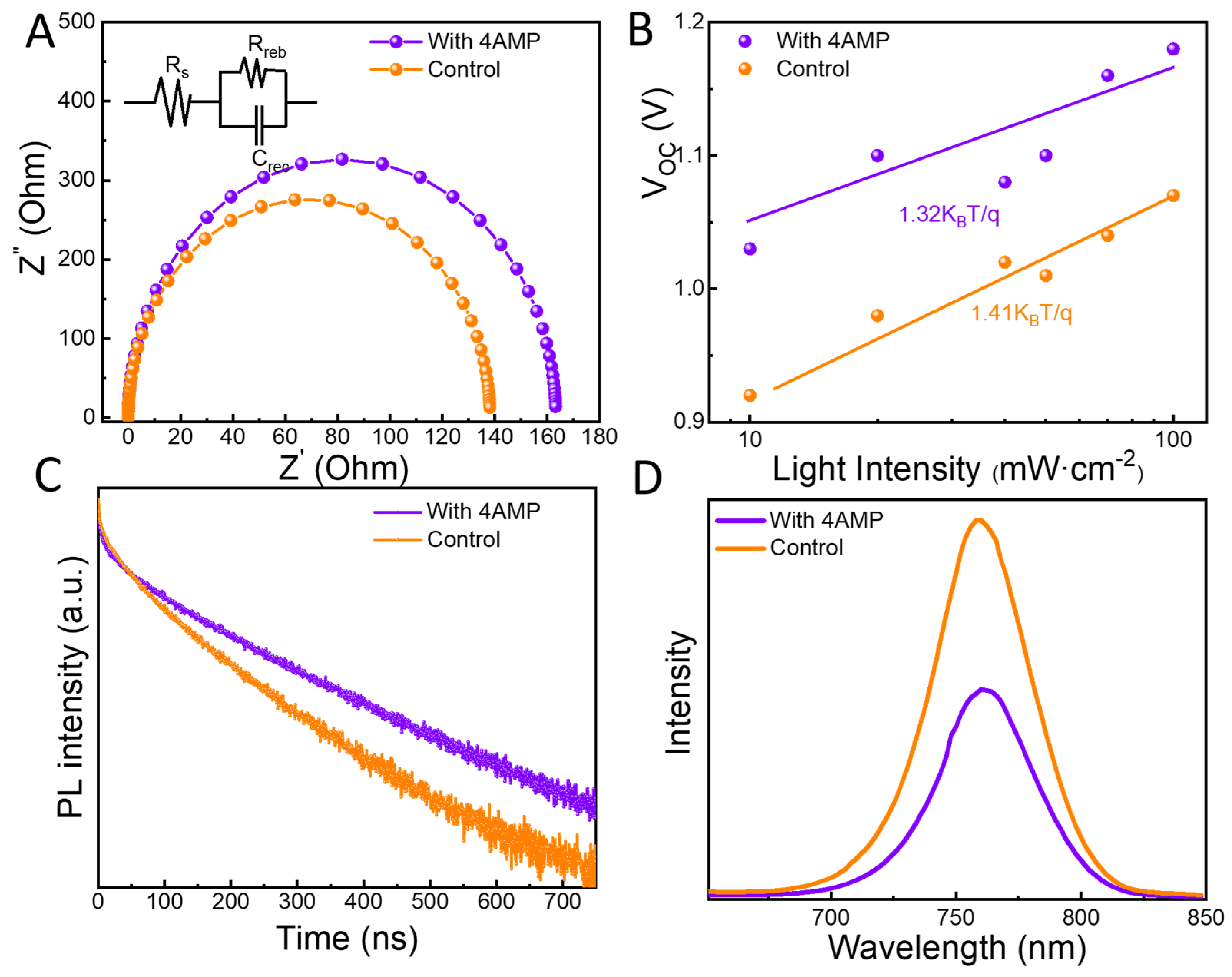
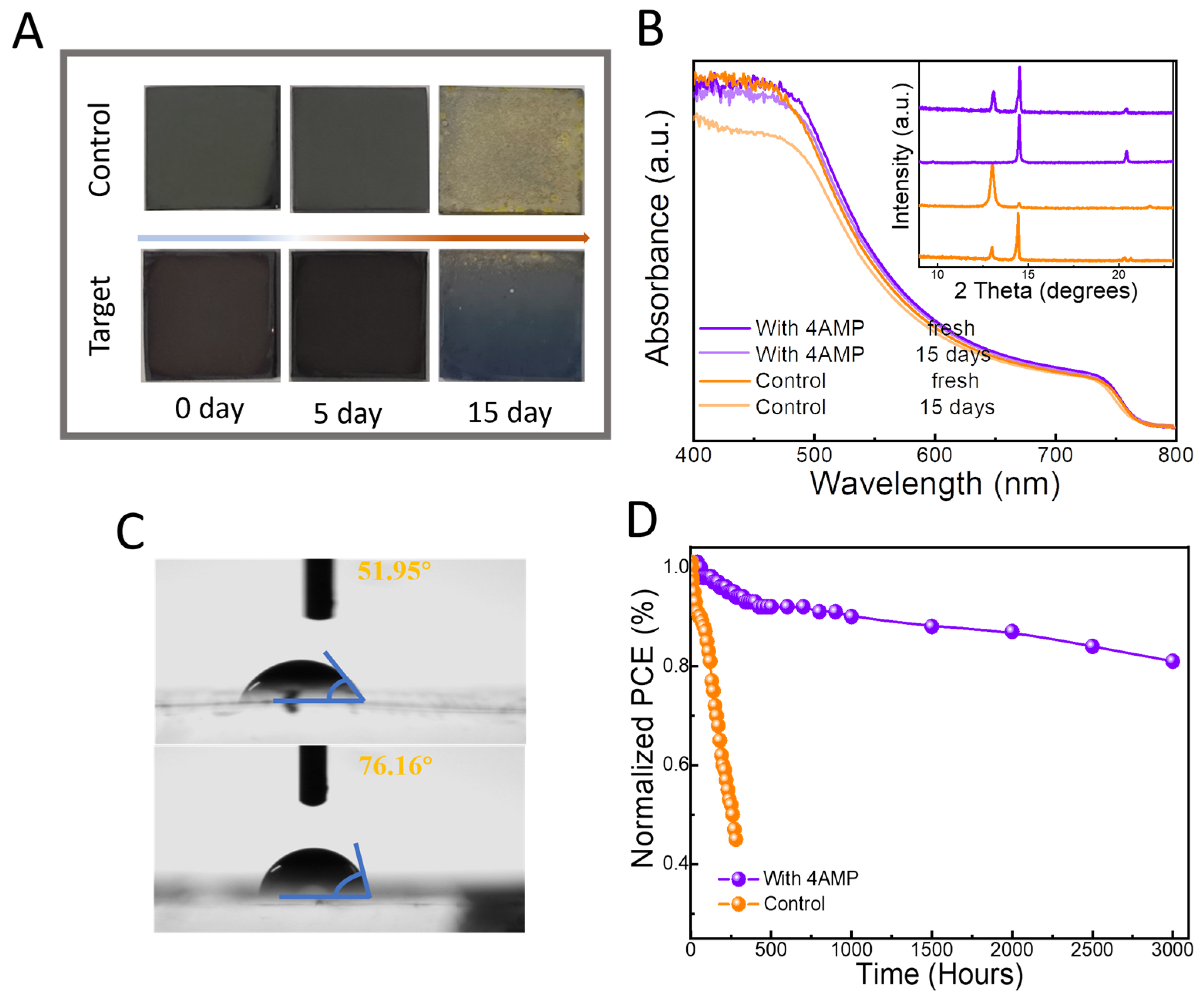
2.1. Morphology
2.2. Photovoltaic Performance of the PSC
3. Conclusions
4. Experiment Section
4.1. Materials
4.2. Device Fabrication
4.3. Device Characterizations
Supplementary Materials
Author Contributions
Funding
Data Availability Statement
Conflicts of Interest
References
- Ma, X.; Yang, L.; Shang, X.; Li, M.; Gao, D.; Wu, C.; Zheng, S.; Zhang, B.; Chen, J.; Chen, C.; et al. Grain boundary defect passivation by in situ formed wide-bandgap lead sulfate for efficient and stable perovskite solar cells. Chem. Eng. J. 2021, 426, 130685. [Google Scholar] [CrossRef]
- Chen, C.; Zheng, S.; Song, H. Photon management to reduce energy loss in perovskite solar cells. Chem. Soc. Rev. 2021, 50, 7250–7329. [Google Scholar] [CrossRef] [PubMed]
- Jeon, N.J.; Noh, J.H.; Yang, W.S.; Kim, Y.C.; Ryu, S.; Seo, J.; Seok, S.I. Compositional engineering of perovskite materials for high-performance solar cells. Nature 2015, 517, 476–480. [Google Scholar] [CrossRef] [PubMed]
- Liu, M.Z.; Johnston, M.B.; Snaith, H.J. Efficient planar heterojunction perovskite solar cells by vapour deposition. Nature 2013, 501, 395–398. [Google Scholar] [CrossRef]
- Ummadisingu, A.; Steier, L.; Seo, J.-Y.; Matsui, T.; Abate, A.; Tress, W.; Grätzel, M. The effect of illumination on the formation of metal halide perovskite films. Nature 2017, 545, 208–212. [Google Scholar] [CrossRef]
- Mei, A.; Li, X.; Liu, L.; Ku, Z.; Liu, T.; Rong, Y.; Xu, M.; Hu, M.; Chen, J.; Yang, Y.; et al. A hole-conductor–free, fully printable mesoscopic perovskite solar cell with high stability. Science 2014, 345, 295–298. [Google Scholar] [CrossRef]
- Nie, W.; Tsai, H.; Asadpour, R.; Blancon, J.-C.; Neukirch, A.J.; Gupta, G.; Crochet, J.J.; Chhowalla, M.; Tretiak, S.; Alam, M.A.; et al. High-efficiency solution-processed perovskite solar cells with millimeter-scale grains. Science 2015, 347, 522–525. [Google Scholar] [CrossRef]
- Samuel, D.; Stranks, G.E.E.; Grancini, G.; Menelaou, C.; Alcocer, M.J.P.; Leijtens, T.; Herz, L.M.; Petrozza, A.; Snaith, H.J. Electron-Hole Diffusion Lengths Exceeding 1 Micrometer in an Organometal Trihalide Perovskite Absorber. Science 2013, 342–343, 341–344. [Google Scholar] [CrossRef]
- Yang, W.S.; Park, B.-W.; Jung, E.H.; Jeon, N.J.; Kim, Y.C.; Lee, D.U.; Shin, S.S.; Seo, J.; Kim, E.K.; Noh, J.H.; et al. Iodide management in formamidinium-lead-halide–based perovskite layers for efficient solar cells. Science 2017, 356, 1376–1379. [Google Scholar] [CrossRef]
- Chen, C.; Li, H.; Jin, J.; Cheng, Y.; Liu, D.; Song, H.; Dai, Q. Highly enhanced long time stability of perovskite solar cells by involving a hydrophobic hole modification layer. Nano Energy 2017, 32, 165–173. [Google Scholar] [CrossRef]
- Chen, C.; Li, H.; Jin, J.; Chen, X.; Cheng, Y.; Zheng, Y.; Liu, D.; Xu, L.; Song, H.; Dai, Q. Long-Lasting Nanophosphors Applied to UV-Resistant and Energy Storage Perovskite Solar Cells. Adv. Energy Mater. 2017, 7, 1700758. [Google Scholar] [CrossRef]
- Chen, C.; Liu, D.; Zhang, B.; Bi, W.; Li, H.; Jin, J.; Chen, X.; Xu, L.; Song, H.; Dai, Q. Carrier Interfacial Engineering by Bismuth Modification for Efficient and Thermoresistant Perovskite Solar Cells. Adv. Energy. Mater. 2018, 8, 201703659. [Google Scholar] [CrossRef]
- Chen, J.; Zhao, X.; Kim, S.G.; Park, N.G. Multifunctional Chemical Linker Imidazoleacetic Acid Hydrochloride for 21% Efficient and Stable Planar Perovskite Solar Cells. Adv. Mater. 2019, 31, e1902902. [Google Scholar] [CrossRef] [PubMed]
- Kim, G.-W.; Kang, G.; Kim, J.; Lee, G.-Y.; Kim, H.I.; Pyeon, L.; Lee, J.; Park, T. Dopant-free polymeric hole transport materials for highly efficient and stable perovskite solar cells. Energy Environ. Sci. 2016, 9, 2326–2333. [Google Scholar] [CrossRef]
- Leijtens, T.; Eperon, G.E.; Pathak, S.; Abate, A.; Lee, M.M.; Snaith, H.J. Overcoming ultraviolet light instability of sensitized TiO2 with meso-superstructured organometal tri-halide perovskite solar cells. Nat. Commun. 2013, 4, 2885. [Google Scholar] [CrossRef] [PubMed]
- Li, M.; Zuo, C.; Hu, J.; Ding, L. Carrier management makes perovskite solar cells approaching Shockley-Queisser limit. Sci. Bull. 2021, 66, 1372–1374. [Google Scholar] [CrossRef] [PubMed]
- Chen, C.; Liu, D.; Wu, Y.; Bi, W.; Sun, X.; Chen, X.; Liu, W.; Xu, L.; Song, H.; Dai, Q. Dual interfacial modifications by conjugated small-molecules and lanthanides doping for full functional perovskite solar cells. Nano Energy 2018, 53, 849–862. [Google Scholar] [CrossRef]
- Chen, C.; Cheng, Y.; Dai, Q.; Song, H. Radio Frequency Magnetron Sputtering Deposition of TiO2 Thin Films and Their Perovskite Solar Cell Applications. Sci. Rep. 2015, 5, 17684. [Google Scholar] [CrossRef]
- Kim, H.; Lee, S.U.; Lee, D.Y.; Paik, M.J.; Na, H.; Lee, J.; Seok, S.I. Optimal Interfacial Engineering with Different Length of Alkylammonium Halide for Efficient and Stable Perovskite Solar Cells. Adv. Energy Mater. 2019, 9, 1902740. [Google Scholar] [CrossRef]
- Yoo, J.J.; Wieghold, S.; Sponseller, M.C.; Chua, M.R.; Bertram, S.N.; Hartono, N.T.P.; Tresback, J.S.; Hansen, E.C.; Correa-Baena, J.-P.; Bulović, V.; et al. An interface stabilized perovskite solar cell with high stabilized efficiency and low voltage loss. Energy Environ. Sci. 2019, 12, 2192–2199. [Google Scholar] [CrossRef]
- Liu, Z.; Qiu, L.; Ono, L.K.; He, S.; Hu, Z.; Jiang, M.; Tong, G.; Wu, Z.; Jiang, Y.; Son, D.-Y.; et al. A holistic approach to interface stabilization for efficient perovskite solar modules with over 2,000-hour operational stability. Nat. Energy 2020, 5, 596–604. [Google Scholar] [CrossRef]
- Yusoff, A.R.b.M.; Nazeeruddin, M.K. Low-Dimensional Perovskites: From Synthesis to Stability in Perovskite Solar Cells. Adv. Energy Mater. 2018, 8, 1702073. [Google Scholar] [CrossRef]
- Cheng, L.; Liu, Z.; Li, S.; Zhai, Y.; Wang, X.; Qiao, Z.; Xu, Q.; Meng, K.; Zhu, Z.; Chen, G. Highly Thermostable and Efficient Formamidinium-Based Low-Dimensional Perovskite Solar Cells. Angew. Chem. Int. Ed. Engl. 2021, 60, 856–864. [Google Scholar] [CrossRef] [PubMed]
- Chen, K.; Wu, P.; Yang, W.; Su, R.; Luo, D.; Yang, X.; Tu, Y.; Zhu, R.; Gong, Q. Low-dimensional perovskite interlayer for highly efficient lead-free formamidinium tin iodide perovskite solar cells. Nano Energy 2018, 49, 411–418. [Google Scholar] [CrossRef]
- Zhao, W.; Dong, Q.; Zhang, J.; Wang, S.; Chen, M.; Zhao, C.; Hu, M.; Jin, S.; Padture, N.P.; Shi, Y. Asymmetric alkyl diamine based Dion–Jacobson low-dimensional perovskite solar cells with efficiency exceeding 15%. J. Mater. Chem. A 2020, 8, 9919–9926. [Google Scholar] [CrossRef]
- Lee, H.B.; Kumar, N.; Devaraj, V.; Tyagi, B.; He, S.; Sahani, R.; Ko, K.-J.; Oh, J.-W.; Kang, J.-W. Trifluoromethyl-Group Bearing, Hydrophobic Bulky Cations as Defect Passivators for Highly Efficient, Stable Perovskite Solar Cells. Sol. RRL 2021, 5, 2100712. [Google Scholar] [CrossRef]
- Lee, H.B.; Kumar, N.; Tyagi, B.; He, S.; Sahani, R.; Kang, J.W. Bulky organic cations engineered lead-halide perovskites: A review on dimensionality and optoelectronic applications. Mater. Today Energy 2021, 21, 100759. [Google Scholar] [CrossRef]
- Zai, H.; Su, J.; Zhu, C.; Chen, Y.; Ma, Y.; Zhang, P.; Ma, S.; Zhang, X.; Xie, H.; Fan, R.; et al. Sandwiched electrode buffer for efficient and stable perovskite solar cells with dual back surface fields. Joule 2021, 5, 2148–2163. [Google Scholar] [CrossRef]
- Wei, N.; Chen, Y.; Miao, Y.; Zhang, T.; Wang, X.; Wei, H.; Zhao, Y. 5-Ammonium Valeric Acid Iodide to Stabilize MAPbI3 via a Mixed-Cation Perovskite with Reduced Dimension. J. Phys. Chem. Lett. 2020, 11, 8170–8176. [Google Scholar] [CrossRef]
- Wang, Y.; Zhang, T.; Kan, M.; Zhao, Y. Bifunctional Stabilization of All-Inorganic alpha-CsPbI3 Perovskite for 17% Efficiency Photovoltaics. J. Am. Chem. Soc. 2018, 140, 12345–12348. [Google Scholar] [CrossRef]
- Sutanto, A.A.; Drigo, N.; Queloz, V.I.E.; Garcia-Benito, I.; Kirmani, A.R.; Richter, L.J.; Schouwink, P.A.; Cho, K.T.; Paek, S.; Nazeeruddin, M.K.; et al. Dynamical evolution of the 2D/3D interface: A hidden driver behind perovskite solar cell instability. J. Mater. Chem. A 2020, 8, 2343–2348. [Google Scholar] [CrossRef]
- Proppe, A.H.; Johnston, A.; Teale, S.; Mahata, A.; Quintero-Bermudez, R.; Jung, E.H.; Grater, L.; Cui, T.; Filleter, T.; Kim, C.Y.; et al. Multication perovskite 2D/3D interfaces form via progressive dimensional reduction. Nat. Commun. 2021, 12, 3472. [Google Scholar] [CrossRef] [PubMed]
- Liu, Z.; Meng, K.; Wang, X.; Qiao, Z.; Xu, Q.; Li, S.; Cheng, L.; Li, Z.; Chen, G. In Situ Observation of Vapor-Assisted 2D-3D Heterostructure Formation for Stable and Efficient Perovskite Solar Cells. Nano Lett. 2020, 20, 1296–1304. [Google Scholar] [CrossRef] [PubMed]
- Lin, Y.; Bai, Y.; Fang, Y.; Chen, Z.; Yang, S.; Zheng, X.; Tang, S.; Liu, Y.; Zhao, J.; Huang, J. Enhanced Thermal Stability in Perovskite Solar Cells by Assembling 2D/3D Stacking Structures. J. Phys. Chem. Lett. 2018, 9, 654–658. [Google Scholar] [CrossRef] [PubMed]
- Ren, H.; Yu, S.; Chao, L.; Xia, Y.; Sun, Y.; Zuo, S.; Li, F.; Niu, T.; Yang, Y.; Ju, H.; et al. Efficient and stable Ruddlesden–Popper perovskite solar cell with tailored interlayer molecular interaction. Nat. Photonics 2020, 14, 154–163. [Google Scholar] [CrossRef]
- Zheng, X.; Chen, B.; Dai, J.; Fang, Y.; Bai, Y.; Lin, Y.; Wei, H.; Zeng, X.C.; Huang, J. Defect passivation in hybrid perovskite solar cells using quaternary ammonium halide anions and cations. Nat. Energy 2017, 2, 17102. [Google Scholar] [CrossRef]
- Ahmad, S.; Fu, P.; Yu, S.; Yang, Q.; Liu, X.; Wang, X.; Wang, X.; Guo, X.; Li, C. Dion-Jacobson Phase 2D Layered Perovskites for Solar Cells with Ultrahigh Stability. Joule 2019, 3, 794–806. [Google Scholar] [CrossRef]
- Ke, W.; Mao, L.; Stoumpos, C.C.; Hoffman, J.; Spanopoulos, I.; Mohite, A.D.; Kanatzidis, M.G. Compositional and Solvent Engineering in Dion–Jacobson 2D Perovskites Boosts Solar Cell Efficiency and Stability. Adv. Energy Mater. 2019, 9, 1803384s. [Google Scholar] [CrossRef]
- Gong, J.; Hao, M.; Zhang, Y.; Liu, M.; Zhou, Y. Layered 2D Halide Perovskites beyond the Ruddlesden-Popper Phase: Tailored Interlayer Chemistries for High-Performance Solar Cells. Angew. Chem. Int. Ed. Engl. 2022, 61, e202112022. [Google Scholar] [CrossRef]
- Mao, L.; Ke, W.; Pedesseau, L.; Wu, Y.; Katan, C.; Even, J.; Wasielewski, M.R.; Stoumpos, C.C.; Kanatzidis, M.G. Hybrid Dion–Jacobson 2D Lead Iodide Perovskites. J. Am. Chem. Soc. 2018, 140, 3775–3783. [Google Scholar] [CrossRef]

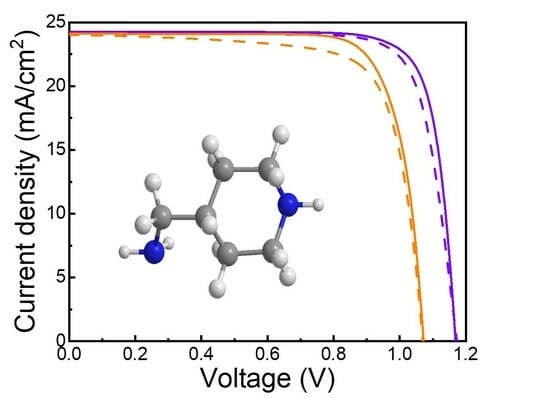
| Samples | Scanning Direction | VOC (V) | JSC (mA·cm−2) | FF (%) | PCE (%) |
| Control | RS | 1.06 | 24.13 | 79.48 | 20.33 |
| FS | 1.06 | 24.07 | 75.25 | 19.20 | |
| With 4AMP | RS | 1.17 | 24.24 | 81.37 | 23.08 |
| FS | 1.17 | 24.17 | 79.06 | 22.36 |
Disclaimer/Publisher’s Note: The statements, opinions and data contained in all publications are solely those of the individual author(s) and contributor(s) and not of MDPI and/or the editor(s). MDPI and/or the editor(s) disclaim responsibility for any injury to people or property resulting from any ideas, methods, instructions or products referred to in the content. |
© 2024 by the authors. Licensee MDPI, Basel, Switzerland. This article is an open access article distributed under the terms and conditions of the Creative Commons Attribution (CC BY) license (https://creativecommons.org/licenses/by/4.0/).
Share and Cite
Bian, J.; Zhang, Y.; Liu, Y.; Pan, X. Leveraging Dion–Jacobson Interface Hierarchies for Defect Alleviation in High-Efficiency and Durable Perovskite Solar Cells. Processes 2024, 12, 233. https://doi.org/10.3390/pr12010233
Bian J, Zhang Y, Liu Y, Pan X. Leveraging Dion–Jacobson Interface Hierarchies for Defect Alleviation in High-Efficiency and Durable Perovskite Solar Cells. Processes. 2024; 12(1):233. https://doi.org/10.3390/pr12010233
Chicago/Turabian StyleBian, Jianxiao, Yuncong Zhang, Yang Liu, and Xiaonan Pan. 2024. "Leveraging Dion–Jacobson Interface Hierarchies for Defect Alleviation in High-Efficiency and Durable Perovskite Solar Cells" Processes 12, no. 1: 233. https://doi.org/10.3390/pr12010233