Article

Synthesis, Characterization and Power Factor Estimation of SnSe Thin Film for Energy Harvesting Applications

1
Sustainable Energy Technologies Center, College of Engineering, King Saud University, Riyadh 11421, Saudi Arabia
2
Mechanical Engineering Department, College of Engineering, King Saud University, P.O. Box 800, Riyadh 11421, Saudi Arabia
3
Department of Physics and Astronomy, College of Science, King Saud University, P.O. Box 2455, Riyadh 11451, Saudi Arabia
4
State Key Laboratory of New Ceramics and Fine Processing, School of Materials Science and Engineering, Tsinghua University, Beijing 100084, China
*
Author to whom correspondence should be addressed.
Processes 2024, 12(4), 665; https://doi.org/10.3390/pr12040665
Submission received: 4 January 2024 / Revised: 31 January 2024 / Accepted: 12 February 2024 / Published: 26 March 2024
(This article belongs to the Section Materials Processes)

Abstract

:
In this work, a simple, cost-effective successive ionic layer adsorption and reaction (SILAR) deposition technique has been used to deposit a high-quality tin selenide (SnSe) thin film onto a glass substrate. Structural, morphologic, and thermoelectric properties have been characterized for the prepared thin film. X-ray diffraction (XRD) results of the SnSe thin film reveal an orthorhombic structure phase. The morphological properties of the prepared thin films have been studied using field emission scanning electron microscopy (FESEM). The stoichiometric composition of the deposited thin film and the elemental binding energies of the Sn and Se elements have been investigated with energy-dispersive spectroscopy (EDS) and X-ray photoelectron spectroscopy (XPS). The Fourier transformation infrared (FTIR) spectrum of the SnSe thin film displays vibrational modes of chalcogenides bonds. These results suggest that the developed thin film is crystalline, uniform, and without impurities and is appropriate for energy harvesting applications. The prepared thin film’s Seebeck coefficient and electrical resistivity were estimated through ZEM-3 from room temperature to 600 K. The power factor was evaluated. A substantially high electrical conductivity is observed, which decreases somewhat with temperature, suggesting a semimetal conducting transport—the absolute values of the Seebeck coefficient increase with temperature. The resulting power factor showed the highest values near room temperature and a somewhat decreasing trend as the temperature increased. Despite lower values of the Seebeck coefficient, the substantially enhanced power factor is due to the higher electrical conductivity of the thin film, superior to that reported previously. This precursor study demonstrates promising results for developing high-performance flexible thermoelectric devices via a simple and facile SILAR strategy.

1. Introduction

Thermoelectric energy harvesting technology provides solutions for sustainable energy challenges, which recycle low-grade waste heat into electricity with the added benefit of reducing greenhouse gas emissions [1,2]. The development of low-cost, high-performance thermoelectric devices is essential to the widespread adoption of this technology [3]. Recently, SnSe came into the limelight in research communities based on its exceptional thermoelectric properties, reported by Zhao and co-workers [2,4]. They proposed alternative strategies to nanostructuring for achieving an exceptionally high figure of merit [4]. In contrast to traditional thermoelectric materials, SnSe is composed of Earth-abundant nontoxic elements and is a simple and stable compound [5]. The crystal structure is layered orthorhombic (Pnma group) and highly anisotropic. At 773 K, the crystal experiences a structural transition from Pnma to Cmcm [4,6]. The maximum ZT~2.6 was observed in the thermoelectric characteristics of SnSe crystals at 923 K along the b-axis, which was attributed to ultralow thermal conductivity induced by gigantic phonon anharmonicity [4,6]. Apparently, this finding is tantamount to earlier innovations in superlattice or nanowire structures that resulted in higher values of ZT. However, industrial applications of SnSe through economically scaled-up processing are still considered a big milestone. Despite the inherent advantage (e.g., low thermal conductivity) of SnSe, which is accounted for by an exceptionally high ZT, SnSe still faces several challenges and requires substantial research activity for its early commercial deployment in the industry.
Several studies have been performed to improve the energy conversion efficiency of polycrystalline materials [7,8,9,10,11,12]. However, the reported ZT values in polycrystalline SnSe are substantially lower than the values observed in single crystals [13]. Some improvements were observed in polycrystalline SnSe by adopting different strategies such as alloying [14], doping [15], and microstructure modulation [16], but most of the ZT values are not larger than ~1 [5].
There are continued efforts for the fabrication of a polycrystalline SnSe thin film through facile and economical routes for applications in flexible thermoelectric materials and the Internet of Things (IoT). Moreover, the strong anisotropy in single-crystal SnSe diverted research toward fabricating textured SnSe thin film to achieve high-performance SnSe materials [17]. Less work has been reported for the development of a thin film based on SnSe materials. For instance, Feng et al. synthesized a SnSe thin film via the rapid microwave plasma chemical vapor deposition method [18]. The thermoelectric characterization showed an improved power factor at 600 K [18]. Similarly, Zhong et al. fabricated highly textured SnSe thin film through a one-step chemical vapor deposition technique and showed an improved power factor at higher temperatures [17]. Most recently, the thermoelectric characteristics of an epitaxially oriented SnSe thin film were investigated by Marjin et al., exhibiting an in-plane Seebeck coefficient similar to single-crystal values, thus leading to an increased power factor [19].
At present, numerous techniques have been used to synthesize SnSe thin films, such as chemical bath deposition [20], sputtering [21], thermal coating [22], hydrothermal deposition [23], pulse laser deposition [24], atomic layer electrochemical epitaxy [24], and electrochemical deposition [25]. Successive ionic layer adsorption and reaction (SILAR) is unique among these deposition methods since it has many advantages [26]. Primarily, it permits the preparation of thin films on a large scale. In addition, the thickness and stoichiometry of the thin films can be precise. Lastly, SILAR is generally an inexpensive technique in terms of application necessities. Klochko et al. [27] reported the deposition of Li-doped NiO films by the SILAR technique and revealed the effects on the structure’s optical, electrical, and thermoelectric characteristics. Kumar et al. synthesized SnSe-based quantum dots through the SILAR method for high-performance solar cells [28]. Farhad et al. [29] described the deposition of cuprous oxide (Cu2O) thin films by a modified SILAR method on both glass and FTO substrates by controlling the pH level of the cationic precursor and the concentration of the anionic precursor to explain their influence on the physical properties of the deposited films. In order to obtain good-quality films, Deshpande et al. [30] reported on the fabrication of a tin disulfide (SnS2) thin film utilizing the SILAR process by varying the cycles, immersion time, rinse time, and deposition temperature. In this study, the deposition, characterization, and power factor estimation of a SILAR-deposited SnSe thin film has been analytically examined. The primary motivation of this research is to deposit nanostructural, uniform, and crystalline SnSe thin films and investigate their thermoelectric properties for energy harvesting applications.

2. Experimental Details

2.1. Chemicals

SnCl2·2H2O (Sigma Aldrich, St. Louis, MO, USA, 99.99%), NaOH (Sigma Aldrich, 99.99%), Se powder (Sigma Aldrich, 99.99%), and Na2SO3 (Sigma Aldrich, 99.99%) were commercially procured.

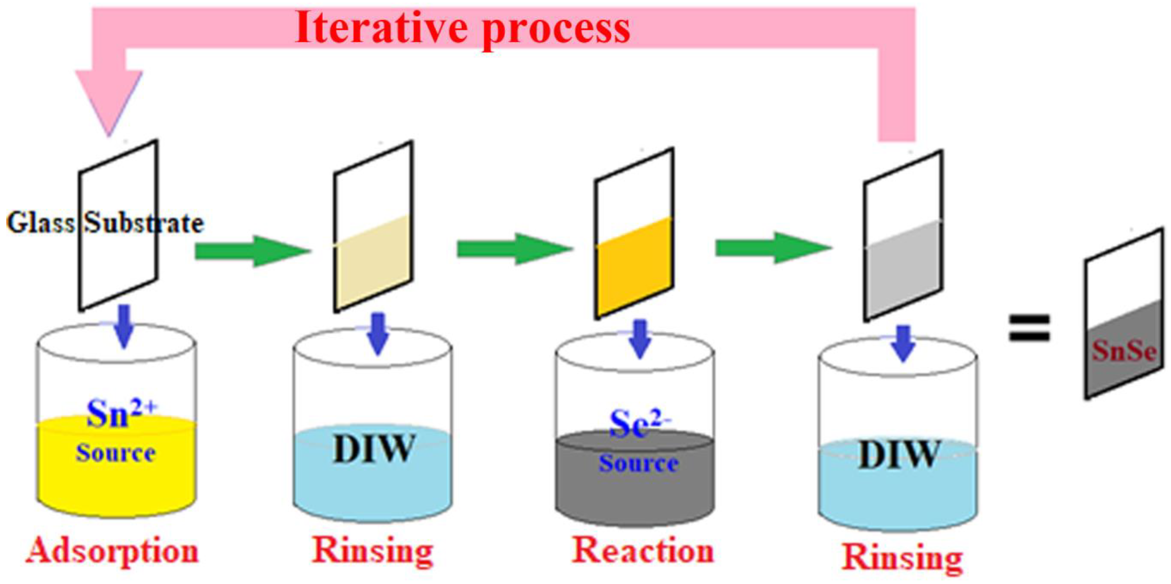
2.2. Preparation of SnSe Thin Film

To deposit the tin selenide (SnSe) thin film, 0.5 M tin chloride (SnCl2·2H2O) was prepared in deionized water. The pH of the solution was adjusted to approximately equal to 11 by the addition of 1 M NaOH, and the prepared solution was used as the cation (Sn2+) source. The other solution, used as the anion (Se2−) source, was sodium selenosulfate (Na2SeSO3), prepared by mixing 2.77 g of sodium sulfite (Na2SO3) with 0.107 g of selenium powder in 50 mL of deionized water (DIW) for 6 h at 80 °C. The clean soda–lime glass substrates were dipped in the cation source solution for 30 s to adsorb Sn2+ ions on the substrate surface. After that, the substrate was washed with deionized water for 10 s to eliminate loosely bound Sn2+ ions. Then, the pre-adsorbed substrate was immersed in the Se2− source solution for 30 s for the reaction of Se2− ions with Sn2+ ions to deposit the SnSe thin film. The unreacted ions were removed by rinsing in DIW for 10 s. Consequently, a SILAR progression cycle of SnSe deposition was accomplished. This deposition cycle was repeated to grow the SnSe thin film to the preferred thickness as shown in Figure 1.
The thickness of the prepared SnSe thin film was measured using the gravimetric method.
t = M ρ A
where ‘M’ is the deposited mass of SnSe in grams, ‘A’ is the area of the thin film in cm2, and ‘ρ’ is the mass density of SnSe (6.18 g/cm3). The measured thickness of the film is about 161.8 nm [31].

2.3. Thin Film Characterization

The structural phase identification of the deposited SnSe thin film was performed by monochromatic PANalytical X’Pert Pro diffractometer with a CuKα X-ray source (wavelength λ = 1.5418 Å). The XRD data were analyzed with highscore pluse software version 3.0e. The vibration modes of the prepared thin film were assessed by FTIR spectroscopy (Perkin Elmer 3 FT-NIR, Waltham, MA, USA). The morphology of the thin film was studied by the FESEM (JEOL JSM-7800F) microscope. The grain size of the thin film was estimated with Image–J software version 1.54. The composition of the prepared thin film was measured using the Oxford Instruments energy-dispersive X-ray analysis (EDAX) facility (Oxford xMax, Abingdon, Oxfordshire, UK) attached to the FE-SEM. The binding energy of the deposited materials was measured using X-ray photoelectron spectroscopy (JPS-9030).

2.4. Thermoelectric Characterization

ZEM-3 from ULVAC Rikco, Yokohama, Japan was employed to evaluate the Seebeck coefficient and electrical conductivity of the thin film using a thin film adapter provided by the company. The thin film samples were mounted on an alumina pillar and connected at both ends with the electrodes through nickel foil caps. Using the static DC method (ULVAC, ZEM-3) in a He environment, the Seebeck coefficient and electrical resistivity were measured from room temperature to ~600 K and at temperature gradients of 20, 30, and 40. All measurements were taken carefully after ensuring the thin film samples were chemically and thermally stable at higher temperatures. The thermoelectric parameters were evaluated using the ZEM series analysis software version 1.01.

3. Results and Discussion

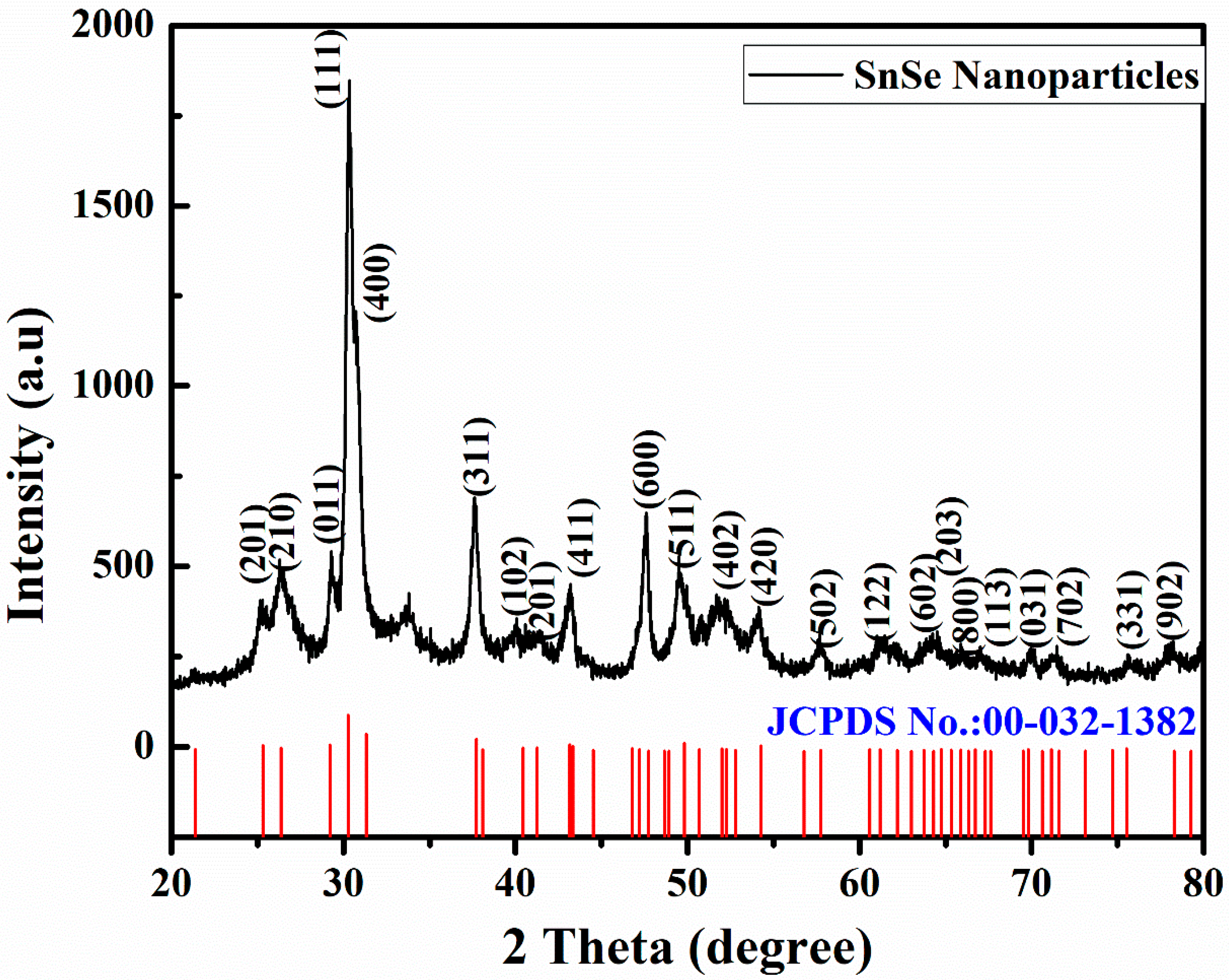
3.1. Structural Analysis

The XRD results of the deposited SnSe thin film and the powder spectra of SnSe described with analogous plans (hkl) are depicted in Figure 2. The indexed diffraction peaks in the XRD pattern correspond to the orthorhombic SnSe structural phase with space group Pnma (JCPDS No.: 00-032-1382) represented by the red lines in Figure 2. Similar structure phase studies by Zainal et al. using the SILAR technique have been reported [32]. The spectrum reveals that the primary dominant peak diffraction is (111), demonstrating a clear association with the consistency of the SnSe thin film.
The structural parameters of the deposited SnSe have been computed using the following equations [33,34]:
D = 0.94 λ β c o s θ
1 d 2 = h 2 a 2 + k 2 b 2 + l 2 c 2
ε = β 4 tan θ
δ = 1 D 2
where ‘D’ is the crystallite size, ‘λ’ is the wavelength of Cu-Kα = 1.5406 Å’ X-rays, ‘2θ’ is the peak position in radians, ‘d’ is the spacing between the plans, ‘β’ is full width at half maximum of the dominant peak, (h, k, l) are the indices of the planes, and (a, b, c) is the lattice constant. Table 1 provides the estimated nanostructure parameters obtained from XRD.
The prepared SnSe thin film was also examined by FTIR spectroscopy to support the pureness of the deposited SnSe and endorse the absorption modes. Figure 3 depicts the FTIR spectra of the deposited thin film at ambient temperature, which were obtained in the 500–4000 cm−1 range. The occurrence of an extensive peak at 3401.50 cm−1 is related to OH [35], and the absorption modes’ presence in the range of 818–1525 cm−1 corresponds to chalcogenide bonding [36]. The intense vibration peak at 604.75 cm−1 might be attributed to the Sn-Se bonding [37]. The water that was absorbed from the air may be the cause of the absorption peak at 1667.88 cm−1 [38].
XPS analysis has been accomplished to investigate the chemical stoichiometry of the SnSe thin film. The XPS spectra (Figure 4a) disclose the presence of both Sn and Se elements in the deposited thin film. The groups present at 54.3 and 56.5 eV are analogous to Se-3d3/2 and Se-3d5/2, corresponding to the occurrence of 2 valency of selenium, as depicted in Figure 4b. The existence of Sn-3d is revealed in Figure 4c, which can be allocated at about 485.7 eV and 494.4 eV, ascribed to Sn-3d5/2 and Sn-3d3/2, respectively. It describes that the tin has 2+ valency. According to the XPS data, Sn and Se showed 2+ and 2 valence locations, respectively.

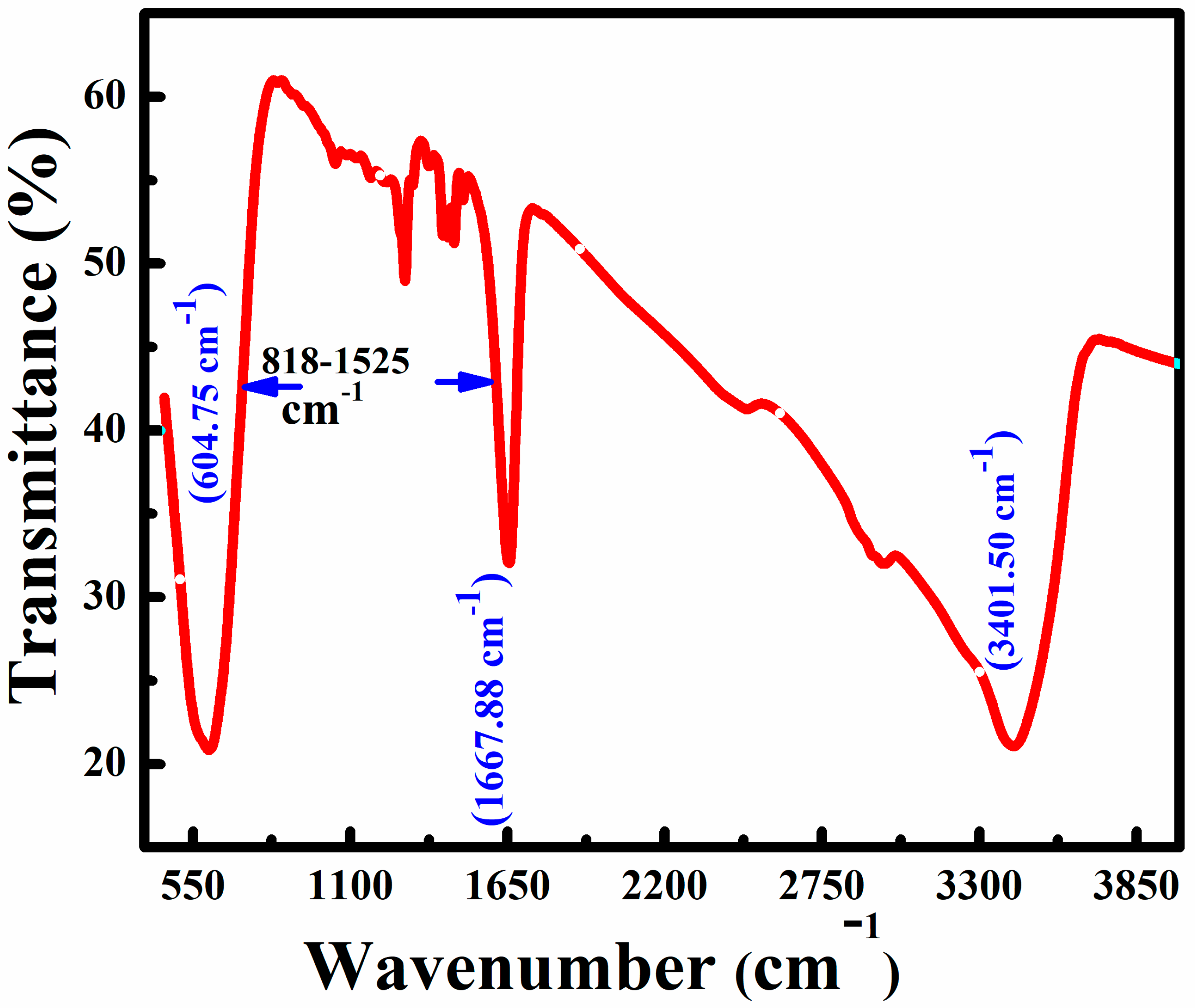
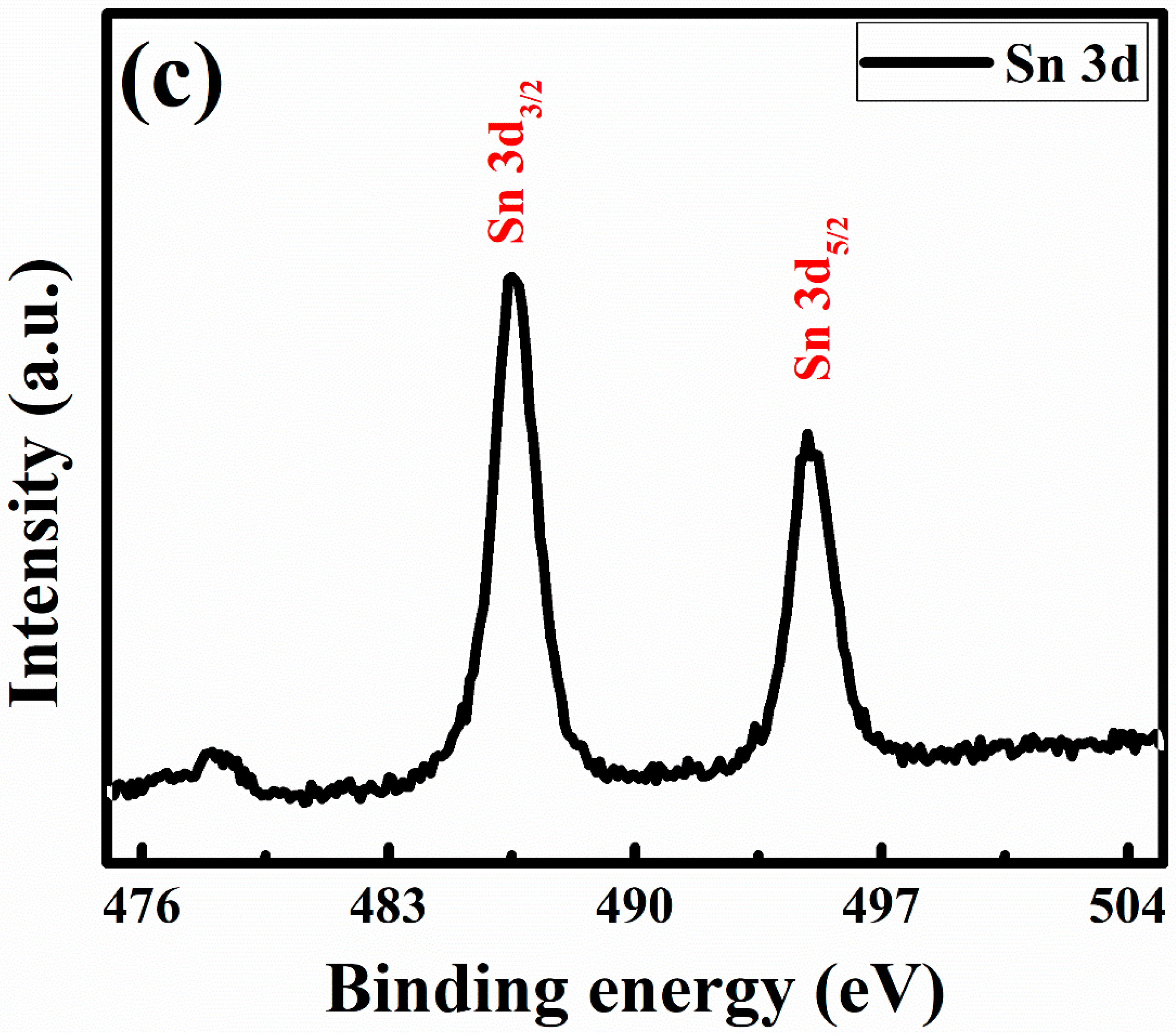
3.2. Surface and Composition Investigations

The peak centered at 495 eV is attributed to Sn-O bonding. It can be assumed that the O 1 s peak appeared because the grain surface of the SnSe thin film was exposed to oxygen in laboratory conditions. The XPS results agree with the conclusions reported for high-performance n-type SnSe synthesized by the arc-melting technique [39].
The morphological investigations of the prepared SnSe thin film were carried out using FESEM. From the FESEM image in Figure 5a, it is detected that the deposited thin film is uniformly deposited on the whole surface and is smooth without cracks. Furthermore, the micrographs of the thin films exposed almost regular nano-sized granular shape grains closely packed together to form bigger spherical structures. The grain size dispersion exposed that the average size is 132 nm, as measured with ImageJ software and shown in Figure 5b.
The elemental composition of the SnSe thin film was measured by EDX analysis, as shown in Figure 6a. Figure 6a establishes that the SnSe consisted of weight fractions of Sn and Se of 56.43 and 43.47%, respectively. The EDX result shows no impurities in the thin film deposited. The EDX mapping investigation (Figure 6b) also discloses a uniform distribution of Sn and Se.

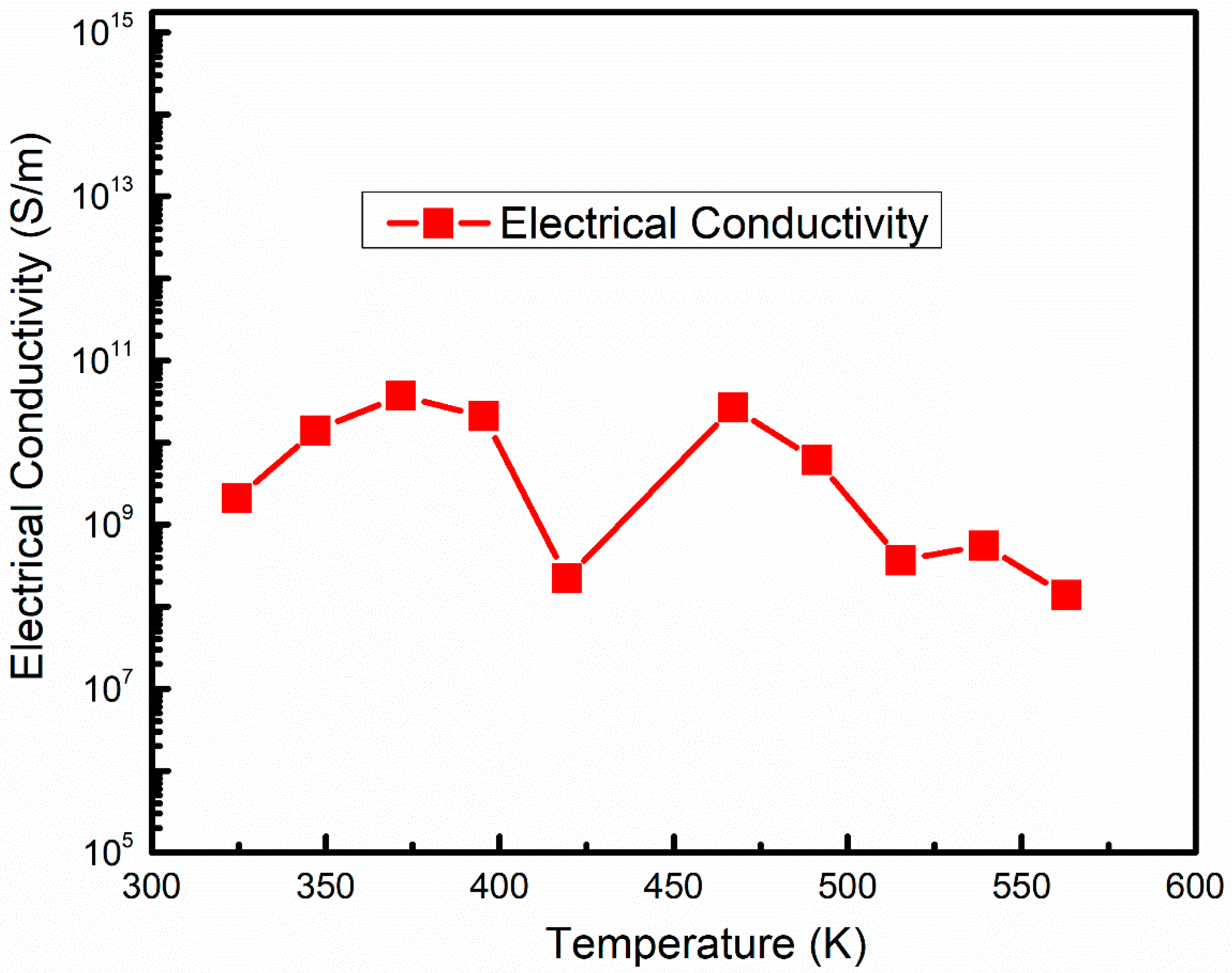
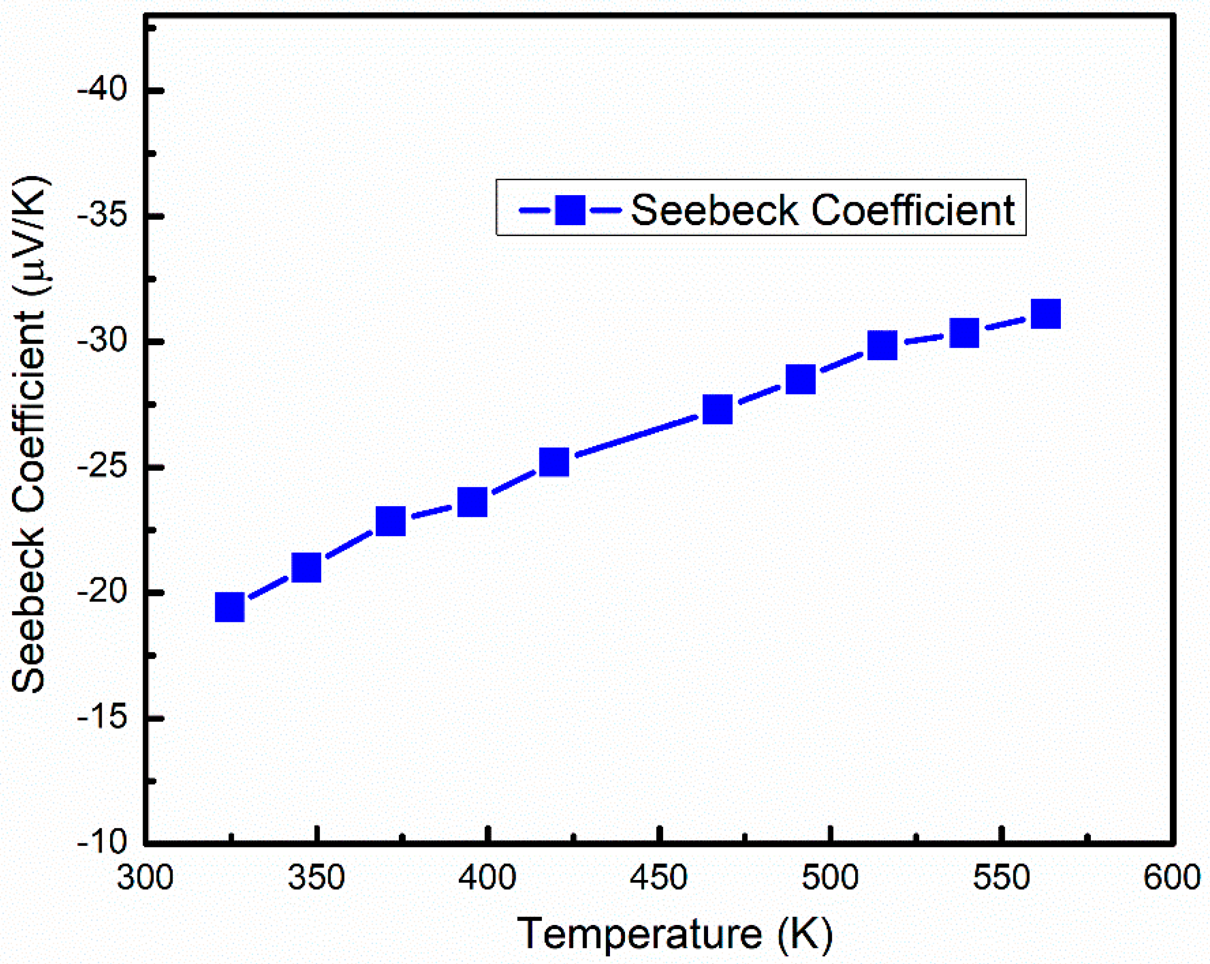
3.3. Thermoelectric Properties

The electrical resistivity and Seebeck coefficient were measured through ZEM-3 simultaneously from room temperature to ~600 K. The thin film demonstrates decreasing electrical conductivity values with the increase in temperature as shown in Figure 7. This behavior suggests the semimetal conducting behavior of the thin film.
The drop in electrical conductivity and subsequent rise with temperature has been reportedly previously in SnSe single crystals [40]. The decreasing and increasing electrical conductivity behavior with temperature is more significant in polycrystalline materials than in single crystals. It is highlighted that SnSe polycrystals exhibit this kind of behavior similar to hysteresis during heating and cooling due to some reversible processes, as observed in several studies [40]. This implies that there could be competing factors between semiconducting and metallic phases in the different temperature ranges, as described by Kuma et al. [41]. The electrical conductivity increases with temperature up to ~400 K, followed by a dip in the value at ~425, suggesting the dominance of semiconducting and metallic characteristics over different temperature regimes. This conductivity trend agrees well with several studies of SnSe-based materials exhibiting similar electrical conductivity behavior with temperature [40,41,42].
The electrical conductivity values are substantially higher than usually reported in the literature. The increase in electrical conductivity values is believed to be partly due to higher values of carrier concentration and partly due to the higher mobility of the charge carriers.
It is well established that electrical conductivity is closely related to carrier concentration and mobility through the relation σ = μ*e*n, where μ is the mobility of the charge carriers, q is the charge, and ‘n’ is the carrier concentration. It can be deduced that an increase in the value of n and/or mobility is the only way to impact the electrical conductivity values in the thin film directly. Duon et al. [43] conducted a similar study by preparing an n-type SnSe2 thin film on an alumina substrate. They attributed the higher electrical conductivity values to the higher carrier concentration. Moreover, Gu et al. [44] related the higher values of electrical conductivity to the higher values of carrier concentration in n-type SnSe polycrystals, which agrees with our results for electrical conductivity. It can be deduced that the higher electrical conductivity values could be primarily attributed to the higher carrier concentration values in this study in accordance with the literature [43,44].
A similar result of a dramatic increase in the electrical conductivity of an n-type SnSe polycrystalline material was reported by Guo et al. [44]. They attributed the substantial increase in the electrical conductivity values to higher concentrations of the charge carriers [44]. The substantial increase in the electrical conductivity values is similar to a previous report [45].
The temperature-dependent Seebeck coefficient of the thin film is shown in Figure 8. The negative sign of the values suggests that most of the charge carriers are composed of electrons. The absolute values of the Seebeck coefficient increase with temperature. The highest value of the Seebeck coefficient is ~30 µV/K. Our values of the Seebeck coefficients are substantially lower than the reported values in the literature for this thin film [46].
The Seebeck coefficient mainly depends on the carrier concentration, carrier effective mass, and temperature. The higher electrical conductivity values are generally considered to be the effect of an increase in carrier concentration, which is consistent with the lower values of the Seebeck coefficient in this study [19]. This suggests that the substantially lower values of Seebeck coefficients agree with the higher electrical conductivity values of the thin film, as both thermoelectric parameters have an inverse relationship with carrier concentration [47].
In a similar study for low-temperature applications, Urmila et al. fabricated a SnSe thin film on a glass substrate using the reactive evaporation method [48]. The group evaluated the Seebeck coefficient and electrical conductivity at lower temperatures up to 300 K. A dramatic increase in the Seebeck coefficient was observed below 84 K. This behavior was attributed to the effect of phonon drags on the charge carriers. In addition, this enhancement resulted from phonon interactions with the mobile charge carriers, and both carriers were combinedly responsible for the unprecedented increase in the Seebeck coefficient [48]. Consequently, an enhanced power factor of the SnSe thin film was achieved.
The resulting values of the power factors as a function of temperature are shown in Figure 9. The power factor has been improved substantially due to the huge electrical conductivity. Compared to the present study, Song et al. reported lower power factor values for a SnSe thin film fabricated by single-target magnetron sputtering [46]. The highest values of power factors are achieved at ~375 and ~470 K. The result suggests that the higher electrical conductivity values could result from the SILAR fabrication method, which formed a completely smooth surface of thin film without cracks, as shown in the SEM image in Figure 5a. Furthermore, the almost regular nano-sized granular-shaped grains closely packed together to form bigger spherical structures are also favorable for smooth carrier transport in the thin film, which could be responsible for the higher mobility of the charge carriers.
The carrier mobility and concentration in SnSe polycrystalline thin film are believed to be considerably higher than the reported results. In general, the counterpart studies show lower values of electrical conductivity due to the strong anisotropy and large number of defects generally observed in polycrystalline SnSe caused by the segregation of Sn [4,5,13]. In contrast, our study shows a considerably improved power factor due to the excellent formation of the thin film using the SILAR method.

4. Conclusions

A SnSe thin film was deposited by the SILAR method on glass substrates for evaluations of structural, morphological, and thermoelectric properties. Several investigative tools were used to evaluate the prepared thin film’s structural phase, chemical bonding, morphological details, and thermoelectric properties. XRD investigation reveals that the SnSe thin film shows an orthorhombic structure, and the crystallite size of the prepared film is about 108.54 nm. The scanning electron microscope image reveals that the SnSe is regularly dispersed on the glass substrate. The prepared materials have deliberately closely packed nanostructures of an average grain size of 132 nm. The elemental investigation and the structural bonding of the film were determined from XPS, EDS, and FTIR analysis. From the FTIR spectra, a broad peak at 818–1525 cm−1 is related to the absorption modes corresponding to chalcogenide bonding. The thermoelectric properties of the thin film were estimated using ZEM-3 from room temperature to ~600 K. The electrical conductivity, in general, decreases with temperature, suggesting a semimetallic conducting behavior. The substantially higher conductivity values suggest an increased concentration and mobility of charge carriers in the thin film.
In contrast, lower values of the Seebeck coefficient are observed in agreement with the literature, and its values increase with temperature increase. The results suggest that substantially improved carrier concentration and mobility could be the prime factors for a higher electrical conductivity of the thin film. Consequently, superior values of the power factor were observed.

Author Contributions

Conceptualization, K.A.; Methodology, K.A.; Software, A.S.; Formal analysis, K.A., S.M.A., R.A. and C.W.; Investigation, K.A. and S.M.A.; Resources, Z.A. and R.A.; Data curation, A.S.; Writing—original draft, S.M.A.; Writing—review & editing, K.A. and Z.A.; Supervision, C.W.; Project administration, Z.A.; Funding acquisition, K.A. All authors have read and agreed to the published version of the manuscript.

Funding

This research was funded by Deputyship for Research & Innovation, Ministry of Education in Saudi Arabia (IFKSUDR_E145).

Data Availability Statement

Data are contained within the article.

Acknowledgments

The authors extend their appreciation to the Deputyship for Research & Innovation, “Ministry of Education” in Saudi Arabia, for funding this research work through the project number (IFKSUDR_E145).

Conflicts of Interest

The authors declare no conflict of interest.

References

  1. Snyder, G.J.; Toberer, E.S. Complex thermoelectric materials. Nat. Mater. 2008, 7, 105–114. [Google Scholar] [CrossRef] [PubMed]
  2. Chen, Z.-G.; Shi, X.; Zhao, L.-D.; Zou, J. High-performance SnSe thermoelectric materials: Progress and future challenge. Prog. Mater. Sci. 2018, 97, 283–346. [Google Scholar] [CrossRef]
  3. Hao, F.; Qiu, P.; Tang, Y.; Bai, S.; Xing, T.; Chu, H.-S.; Zhang, Q.; Lu, P.; Zhang, T.; Ren, D.; et al. High efficiency Bi2Te3-based materials and devices for thermoelectric power generation between 100 and 300 °C. Energy Environ. Sci. 2016, 9, 3120–3127. [Google Scholar] [CrossRef]
  4. Zhao, L.-D.; Lo, S.-H.; Zhang, Y.; Sun, H.; Tan, G.; Uher, C.; Wolverton, C.; Dravid, V.P.; Kanatzidis, M.G. Ultralow thermal conductivity and high thermoelectric figure of merit in SnSe crystals. Nature 2014, 508, 373. [Google Scholar] [CrossRef] [PubMed]
  5. Zhao, L.-D.; Chang, C.; Tan, G.; Kanatzidis, M.G. SnSe: A remarkable new thermoelectric material. Energy Environ. Sci. 2016, 9, 3044–3060. [Google Scholar] [CrossRef]
  6. Zhao, L.-D.; Tan, G.; Hao, S.; He, J.; Pei, Y.; Chi, H.; Wang, H.; Gong, S.; Xu, H.; Dravid, V.P.; et al. Ultrahigh power factor and thermoelectric performance in hole-doped single-crystal SnSe. Science 2016, 351, 141–144. [Google Scholar] [CrossRef]
  7. Asfandiyar; Li, Z.L.; Sun, F.H.; Tang, H.C.; Dong, J.F.; Li, J.F. Enhanced thermoelectric properties of p-type SnS0.2Se0.8 solid solution doped with Ag. J. Alloys Compd. 2018, 745, 172–178. [Google Scholar] [CrossRef]
  8. Hamad, B. Electronic and Thermoelectric Properties of SnSe1-x S (x) (x=0, 0.25, 0.5, 0.75, and 1) Alloys: First-Principles Calculations. J. Electron. Mater. 2018, 47, 4047–4055. [Google Scholar] [CrossRef]
  9. Li, Q.Q.; Zhang, L.L.; Yin, J.Z.; Sheng, Z.H.; Chu, X.Z.; Wang, F.; Zhu, F.X. Study on the thermoelectric performance of polycrystal SnSe with Se vacancies. J. Alloys Compd. 2018, 745, 513–518. [Google Scholar] [CrossRef]
  10. Melendez, J.J.; Gonzalez-Romero, R.L. zT factors in Ag- and Na-doped SnSe: Chemical potentials, relaxation times and predictions for other dopant species. J. Alloys Compd. 2018, 757, 70–78. [Google Scholar] [CrossRef]
  11. Peng, Z.; He, D.Q.; Mu, X.; Zhou, H.Y.; Li, C.C.; Ma, S.F.; Ji, P.X.; Hou, W.K.; Wei, P.; Zhu, W.T.; et al. Preparation and Enhanced Thermoelectric Performance of Cu2Se-SnSe Composite Materials. J. Electron. Mater. 2018, 47, 3350–3357. [Google Scholar] [CrossRef]
  12. Shu, Y.J.; Su, X.L.; Xie, H.Y.; Zheng, G.; Liu, W.; Yan, Y.G.; Luo, T.T.; Yang, X.; Yang, D.W.; Uher, C.; et al. Modification of Bulk Heterojunction and CI Doping for High-Performance Thermoelectric SnSe2/SnSe Nanocomposites. ACS Appl. Mater. Interfaces 2018, 10, 15793–15802. [Google Scholar] [CrossRef]
  13. Li, S.; Li, X.; Ren, Z.; Zhang, Q. Recent progress towards high performance of tin chalcogenide thermoelectric materials. J. Mater. Chem. A 2018, 6, 2432–2448. [Google Scholar] [CrossRef]
  14. Wei, T.-R.; Tan, G.; Wu, C.-F.; Chang, C.; Zhao, L.-D.; Li, J.-F.; Snyder, G.J.; Kanatzidis, M.G. Thermoelectric transport properties of polycrystalline SnSe alloyed with PbSe. Appl. Phys. Lett. 2017, 110, 053901. [Google Scholar] [CrossRef]
  15. Tang, G.; Wei, W.; Zhang, J.; Li, Y.; Wang, X.; Xu, G.; Chang, C.; Wang, Z.; Du, Y.; Zhao, L.-D. Realizing High Figure of Merit in Phase-Separated Polycrystalline Sn1–xPbxSe. J. Am. Chem. Soc. 2016, 138, 13647–13654. [Google Scholar] [CrossRef] [PubMed]
  16. Fu, Y.; Xu, J.; Liu, G.-Q.; Yang, J.; Tan, X.; Liu, Z.; Qin, H.; Shao, H.; Jiang, H.; Liang, B.; et al. Enhanced thermoelectric performance in p-type polycrystalline SnSe benefiting from texture modulation. J. Mater. Chem. C 2016, 4, 1201–1207. [Google Scholar] [CrossRef]
  17. Zhong, Y.; Zhang, L.; Linseis, V.; Qin, B.; Chen, W.; Zhao, L.-D.; Zhu, H. High-quality textured SnSe thin films for self-powered, rapid-response photothermoelectric application. Nano Energy 2020, 72, 104742. [Google Scholar] [CrossRef]
  18. Feng, Y.; Zhang, X.; Lei, L.; Nie, Y.; Xiang, G. Rapid synthesis of thermoelectric SnSe thin films by MPCVD. RSC Adv. 2020, 10, 11990–11993. [Google Scholar] [CrossRef] [PubMed]
  19. van de Putte, M.W.; Huijben, M. Epitaxial tin selenide thin film thermoelectrics. Appl. Surf. Sci. 2023, 623, 157034. [Google Scholar] [CrossRef]
  20. Price, L.S.; Parkin, I.P.; Hardy, A.M.E.; Clark, R.J.H.; Hibbert, T.G.; Molloy, K.C. Atmospheric Pressure Chemical Vapor Deposition of Tin Sulfides (SnS, Sn2S3, and SnS2) on Glass. Chem. Mater. 1999, 11, 1792–1799. [Google Scholar] [CrossRef]
  21. Hartman, K.; Johnson, J.L.; Bertoni, M.I.; Recht, D.; Aziz, M.J.; Scarpulla, M.A.; Buonassisi, T. SnS thin-films by RF sputtering at room temperature. Thin Solid Films 2011, 519, 7421–7424. [Google Scholar] [CrossRef]
  22. Ogah, O.E.; Reddy, K.R.; Zoppi, G.; Forbes, I.; Miles, R.W. Annealing studies and electrical properties of SnS-based solar cells. Thin Solid Films 2011, 519, 7425–7428. [Google Scholar] [CrossRef]
  23. Zhu, H.; Yang, D.; Ji, Y.; Zhang, H.; Shen, X. Two-dimensional SnS nanosheets fabricated by a novel hydrothermal method. J. Mater. Sci. 2005, 40, 591–595. [Google Scholar] [CrossRef]
  24. Teghil, R.; Santagata, A.; Marotta, V.; Orlando, S.; Pizzella, G.; Giardini-Guidoni, A.; Mele, A. Characterization of the plasma plume and of thin film epitaxially produced during laser ablation of SnSe. Appl. Surf. Sci. 1995, 90, 505–514. [Google Scholar] [CrossRef]
  25. Gregory, B.W.; Stickney, J.L. Electrochemical atomic layer epitaxy (ECALE). J. Electroanal. Chem. Interfacial Electrochem. 1991, 300, 543–561. [Google Scholar] [CrossRef]
  26. Burton, M.R.; Boyle, C.A.; Liu, T.; McGettrick, J.; Nandhakumar, I.; Fenwick, O.; Carnie, M.J. Full Thermoelectric Characterization of Stoichiometric Electrodeposited Thin Film Tin Selenide (SnSe). ACS Appl. Mater. Interfaces 2020, 12, 28232–28238. [Google Scholar] [CrossRef] [PubMed]
  27. Klochko, N.P.; Klepikova, K.S.; Zhadan, D.O.; Petrushenko, S.I.; Kopach, V.R.; Khrypunov, G.S.; Lyubov, V.M.; Dukarov, S.V.; Nikitin, V.O.; Maslak, M.O.; et al. Structure, optical, electrical and thermoelectric properties of solution-processed Li-doped NiO films grown by SILAR. Mater. Sci. Semicond. Process. 2018, 83, 42–49. [Google Scholar] [CrossRef]
  28. Kishore Kumar, D.; Loskot, J.; Kříž, J.; Bennett, N.; Upadhyaya, H.M.; Sadhu, V.; Venkata Reddy, C.; Reddy, K.R. Synthesis of SnSe quantum dots by successive ionic layer adsorption and reaction (SILAR) method for efficient solar cells applications. Sol. Energy 2020, 199, 570–574. [Google Scholar] [CrossRef]
  29. Farhad, S.F.U.; Hossain, M.A.; Tanvir, N.I.; Akter, R.; Patwary, M.A.M.; Shahjahan, M.; Rahman, M.A. Structural, optical, electrical, and photoelectrochemical properties of cuprous oxide thin films grown by modified SILAR method. Mater. Sci. Semicond. Process. 2019, 95, 68–75. [Google Scholar] [CrossRef]
  30. Deshpande, N.G.; Sagade, A.A.; Gudage, Y.G.; Lokhande, C.D.; Sharma, R. Growth and characterization of tin disulfide (SnS2) thin film deposited by successive ionic layer adsorption and reaction (SILAR) technique. J. Alloys Compd. 2007, 436, 421–426. [Google Scholar] [CrossRef]
  31. Aldawood, S.; AlGamdi, S.; Salman, S.; Garawi, M.; Alkhuraiji, T.; Ali, S. Influence of γ-ray exposure and dose dependent characteristics of (n)PbS–(p)Si hetero-structure. J. Mater. Sci. Mater. Electron. 2021, 32, 11616–11627. [Google Scholar] [CrossRef]
  32. Zainal, Z.; Saravanan, N.; Anuar, K.; Hussein, M.Z.; Yunus, W.M.M. Chemical bath deposition of tin selenide thin films. Mater. Sci. Eng. B 2004, 107, 181–185. [Google Scholar] [CrossRef]
  33. Zhang, C.; Yin, H.; Han, M.; Dai, Z.; Pang, H.; Zheng, Y.; Lan, Y.Q.; Bao, J.; Zhu, J. Two-dimensional tin selenide nanostructures for flexible all-solid-state supercapacitors. ACS Nano 2014, 8, 3761–3770. [Google Scholar] [CrossRef] [PubMed]
  34. Choi, J.; Jin, J.; Jung, I.G.; Kim, J.M.; Kim, H.J.; Son, S.U. SnSe2 nanoplate–graphene composites as anode materials for lithium ion batteries. Chem. Commun. 2011, 47, 5241–5243. [Google Scholar] [CrossRef] [PubMed]
  35. Pejjai, B.; Minnam Reddy, V.R.; Seku, K.; Pallavolu, M.R.; Park, C. Eco-friendly synthesis of SnSe nanoparticles: Effect of reducing agents on the reactivity of a Se-precursor and phase formation of SnSe NPs. New J. Chem. 2018, 42, 4843–4853. [Google Scholar] [CrossRef]
  36. Rashad, M.M.; Shalan, A.E.; Lira-Cantú, M.; Abdel-Mottaleb, M.S.A. Enhancement of TiO2 nanoparticle properties and efficiency of dye-sensitized solar cells using modifiers. Appl. Nanosci. 2013, 3, 167–174. [Google Scholar] [CrossRef]
  37. Arokiya Mary, T.; Fernandez, A.C.; Sakthivel, P.; Jesudurai, J.G.M. A study on the role of surfactant on the layered growth of SnSe2 for electrical applications. J. Mater. Sci. Mater. Electron. 2016, 27, 11041–11048. [Google Scholar] [CrossRef]
  38. Tanhaei, M.; Mahjoub, A.R.; Safarifard, V. Energy-efficient sonochemical approach for the preparation of nanohybrid composites from graphene oxide and metal-organic framework. Inorg. Chem. Commun. 2019, 102, 185–191. [Google Scholar] [CrossRef]
  39. Gainza, J.; Serrano-Sánchez, F.; Rodrigues, J.E.F.S.; Huttel, Y.; Dura, O.J.; Koza, M.M.; Fernández-Díaz, M.T.; Meléndez, J.J.; Márkus, B.G.; Simon, F.; et al. High-Performance n-type SnSe Thermoelectric Polycrystal Prepared by Arc-Melting. Cell Rep. Phys. Sci. 2020, 1, 100263. [Google Scholar] [CrossRef]
  40. Shi, W.; Gao, M.; Wei, J.; Gao, J.; Fan, C.; Ashalley, E.; Li, H.; Wang, Z. Tin Selenide (SnSe): Growth, Properties, and Applications. Adv. Sci. 2018, 5, 1700602. [Google Scholar] [CrossRef]
  41. Kumar, M.; Rani, S.; Parmar, R.; Amati, M.; Gregoratti, L.; Ghosh, A.; Pathak, S.; Kumar, A.; Wang, X.; Singh, V.N. The ultra-high thermoelectric power factor in facile and scalable single-step thermal evaporation fabricated composite SnSe/Bi thin films. J. Mater. Chem. C 2022, 10, 18017–18024. [Google Scholar] [CrossRef]
  42. Wang, Y.; Qin, B.; Wang, D.-Y.; Hong, T.; Gao, X.; Zhao, L. Realizing high thermoelectric properties in p-type polycrystalline SnSe by inducing DOS distortion. Rare Met. 2021, 40, 2819–2828. [Google Scholar] [CrossRef]
  43. Duong, A.T.; Nguyen, D.L.; Nguyen, M.N.; Nguyen, T.M.H.; Nguyen, A.D.; Pham, A.T.; Ullah, F.; Tahir, Z.; Kim, Y.S.; Trung, D.Q.; et al. High thermoelectric power factor in SnSe2 thin film grown on Al2O3 substrate. Mater. Res. Express 2019, 6, 066420. [Google Scholar] [CrossRef]
  44. Gu, W.-H.; Zhang, Y.-X.; Guo, J.; Cai, J.-F.; Zhu, Y.-K.; Zheng, F.; Jin, L.; Xu, J.; Feng, J.; Ge, Z.-H. Realizing high thermoelectric performance in n-type SnSe polycrystals via (Pb, Br) co-doping and multi-nanoprecipitates synergy. J. Alloys Compd. 2021, 864, 158401. [Google Scholar] [CrossRef]
  45. Li, F.; Wang, W.; Qiu, X.; Zheng, Z.; Fan, P.; Luo, J.; Li, B. Optimization of thermoelectric properties of n-type Ti, Pb co-doped SnSe. Inorg. Chem. Front. 2017, 4, 1721–1729. [Google Scholar] [CrossRef]
  46. Song, L.; Zhang, J.; Iversen, B.B. Enhanced thermoelectric properties of SnSe thin films grown by single-target magnetron sputtering. J. Mater. Chem. A 2019, 7, 17981–17986. [Google Scholar] [CrossRef]
  47. Marfoua, B.; Hong, J. Graphene Induced High Thermoelectric Performance in ZnO/Graphene Heterostructure. Adv. Mater. Interfaces 2023, 10, 2202387. [Google Scholar] [CrossRef]
  48. Urmila, K.S.; Namitha, T.A.; Rajani, J.; Philip, R.R.; Pradeep, B. Optoelectronic properties and Seebeck coefficient in SnSe thin films. J. Semicond. 2016, 37, 093002. [Google Scholar] [CrossRef]
Figure 1. The scheme of SILAR technique for the deposition of SnSe thin film.
Processes 12 00665 g001
Figure 2. XRD result of deposited SnSe thin film.
Processes 12 00665 g002
Figure 3. FTIR spectra of SnSe thin film.
Processes 12 00665 g003
Figure 4. The XPS results: (a) full-range spectrum, (b) Se-3d, and (c) Sn-3d.
Processes 12 00665 g004aProcesses 12 00665 g004b
Figure 5. FESEM micrograph: (a) SnSe thin film and (b) particle distribution of the SnSe thin film.
Processes 12 00665 g005
Figure 6. EDX analysis of (a) SnSe thin film and (b) elemental mappings of SnSe thin film with elements of Sn and Se.
Processes 12 00665 g006
Figure 7. Electrical conductivities of the thin film with temperature.
Processes 12 00665 g007
Figure 8. Seebeck coefficient of the thin film with temperature.
Processes 12 00665 g008
Figure 9. Power factor of the thin film with temperature.
Processes 12 00665 g009
Table 1. Nanostructural parameters of deposited SnSe thin film.
SampleCrystallite Dimension
(nm)
Microstrain
(ε × 10−2)
Deformation Density
(δ) (m−2 × 10¹⁵)
Lattice Constants
a (Å)b (Å)c (Å)
SnSe108.5411.838.484.1734.78611.239
Disclaimer/Publisher’s Note: The statements, opinions and data contained in all publications are solely those of the individual author(s) and contributor(s) and not of MDPI and/or the editor(s). MDPI and/or the editor(s) disclaim responsibility for any injury to people or property resulting from any ideas, methods, instructions or products referred to in the content.

