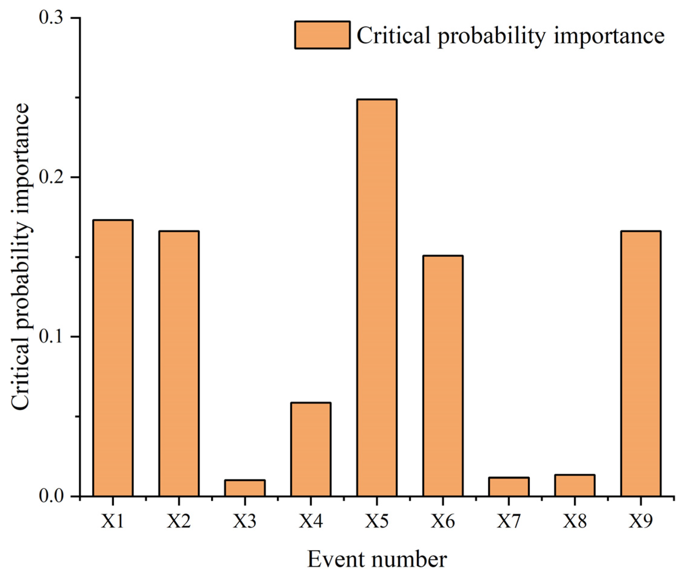
Abstract
As the core component of electronic equipment, vibration load has an important effect on the reliability of circuit boards. However, construction machinery has high requirements for construction efficiency and safety performance, and also has high maintenance costs. In this paper, a vibration reliability analysis and structural optimization of the control circuit board of a drilling rig are conducted. First, Failure Mode, Effects and Criticality Analysis (FMECA) and Fault Tree Analysis (FTA) qualitative and quantitative analysis were used to find the weak links in the circuit board. The quantitative and qualitative analysis results of FMECA and FTA show that the critical probability importance values of the chip inductor and TVS diode short circuit are the highest, at 0.249 and 0.173, respectively. They are up to 0.239 higher than those of the other components. Then, according to the analysis results, a precise simplified model is established for the core components, including the weak links, and modal simulations and modal tests are carried out. The key influencing parameters are obtained through comparative analysis and research on natural frequency and frequency response curves. Finally, the position of the stress–strain sensitive source in the real working environment is determined by a dynamic simulation analysis of the random vibration performance of the finite element model. The results can provide an optimization basis for an anti-vibration design of circuit boards.
1. Introduction
With the gradual development of electronic devices to a modular, high-performance and multi-functional state, their packaging technology also shows a trend of being high-density [1]. During the operational phase, circuit boards are frequently subjected to environmental stresses such as mechanical stress (vibration, impact, etc.) [2], thermal stress (high temperature, low temperature, temperature fluctuations, etc.) [3], electrical stress (over-voltage, over-current, etc.), and chemical corrosion (humidity, salt spray, etc.), which can lead to the failure of the circuit board. Additionally, improper processing and material defects [4] can also contribute to the malfunctioning of circuit boards.
Vibration as a complex load has been the subject of research for a long time [5]. Therefore, it is very important to understand the failure mechanism of components under vibration conditions. Printed Circuit Boards (PCBs) are important components of electronic equipment, and their sensitivity to vibration directly affects the reliability and environmental adaptability of electronic equipment [6].
On a PCB, the solder joint is a key part of signal transmission, mechanical connection and electrical conduction, so solder joint failure is closely related to PCB failure. In order to strengthen the reliability of solder joints, some scholars chose to optimize the solder. Yomamoto et al. [7] investigated the effects of Ni addition on the microstructure, tensile, and fatigue properties of Sn-6.4Sb-3.9Ag (mass%). Li et al. [8] prepared SN-25SB-X Ag (x = 0, 2.5, 3.0, and 3.5, where x is the mass percentage) solder alloys by adding Ag to Sn-25Sb solder. The mechanical properties of the solder joints were improved.
The above research only improved the mechanical properties of solder joints by optimizing the solder. In order to improve the vibration reliability of the whole PCB, it is necessary to design and optimize the key components, solder joint distribution, and substrate structure. Some scholars employed scanning imaging techniques to detect defects in circuit boards. For instance, Wang et al. [9] proposed laser-induced ultrasound scanning imaging, which offers the advantage of high-resolution imaging for small-diameter defects when compared to traditional infrared thermography. With this technology, faults can be detected at an early stage, so repairing the fault area before mass production can prevent damage to the entire board. Some scholars conducted vibration analysis of PCBs through finite element analysis to study its dynamic response characteristics after vibration excitation, or to predict its fatigue life under random vibration load, which can provide a basis for the optimization of PCB design. Muhammad et al. [2] estimated the remaining useful life (RUL) of electronic modules by means of vibration testing and finite element analysis techniques. Karthiheyan et al. [10] used JEDEC standards for an experimental verification of their results, verified the finite element design used for their study, and conducted random vibration experiments through finite element analysis. The fatigue life of PCB under different random vibration environments was predicted and compared.
To sum up, finite element analysis plays an important role in vibration reliability analysis [11,12,13,14,15], but the following problems need to be solved in practical applications: (1) A lack of qualitative and quantitative analysis of fault sample data in specific industries, resulting in an oversimplification of finite element models. (2) The failure mechanisms of actual engineering machinery control systems have not been deeply studied. Aging tests require a long time and high cost, and it is difficult to locate weak links accurately.
In this paper, by comparing the results of the effects and criticality analysis (FMECA), modal experiment, and modal simulation, a finite element model of a rig control circuit board is established. Then, the finite element model is analyzed by random vibration simulation, and its weak links under random vibration loads are obtained, which provide an optimization basis for a vibration reduction design of the PCB. Finally, based on the analysis results, optimization suggestions are put forward. The main novelties and contributions of this study are summarized as follows:
- Through the mutual verification and comparison of the modal experiment, modal simulation, and FMECA, the finite element model is closer to reality.
- The vibration reliability of the rig control circuit board under actual working conditions is analyzed in depth and feasible optimization suggestions are put forward. It is expected to provide fast, accurate, and efficient technical support for the reliability improvement of similar mechanical and electrical products at the use stage.
The rest of this paper is organized as follows: Section 2 introduces the basic theories of FMCEA, FTA, and modal analysis. Section 3 introduces the establishment of the finite element model. In Section 4, the analysis results of the modal and random vibration simulations are given and the optimization suggestions for the rig control circuit board are put forward. Section 5 summarizes the full paper.
2. Theory
2.1. FMECA
Failure Mode, Effects and Criticality Analysis (FMECA) is one of the most effective methods of risk assessment and maintenance management [16]. FMECA has been used to identify critical risk events and predict system failures to avoid or reduce potential failure modes and their effects on operations. FMECA is composed of two separate analyses: Failure Mode and Effects Analysis (FMEA) and Criticality Analysis (CA). FMECA includes a list of possible device failure modes, failure causes, and local and final effects that refer to the impact of each failure on the system element and the whole system, respectively [17]. In this paper, based on the controller circuit board fault records provided by Quzhou Hixee Electronic Technology Co., Ltd. (Quzhou, China), FMECA was used to identify the key components that led to faults in the circuit board system, and these key components were retained when the finite element model was established.
When performing CA, it is necessary to calculate the criticality. The calculation formula is as follows: [18]
where a represents the frequency ratio of the j-th failure mode, represents the impact probability of the j-th failure mode, represents the failure frequency (1/h), and t represents the system working time.
2.2. FTA
FTA uses the deductive principle for analysis, lists the logical relationship of each event, finds the cause of system failure, finds potential problems and reveals weak links, and finally draws a fault tree to determine the occurrence probability of each bottom event. Referring to the analysis results of FMECA, the top events and key bottom events are determined for FTA, which can reduce the analysis time while ensuring accuracy.
When using a fault tree for quantitative analysis, it is necessary to calculate the occurrence probability, structural importance, and probability importance of the top event. When calculating the occurrence probability of the fault tree’s top event accurately, it should be developed according to the probability formula of logical union in the Boolean singular, that is, the exclusion theorem. The formula is [19]:
where represents the probability of occurrence of the i smallest cut set, and indicates the minimum number of cut sets.
After calculating the probability of the top event, it is necessary to analyze the importance of the fault tree. Importance is an index used to evaluate the importance of a single component or function on the whole; especially in Fault Tree Analysis, evaluating the impact of an event on the top event is very important. In this paper, the probabilistic importance and critical probabilistic importance of the fault tree of the circuit board system are studied.
- (1)
- Probability importance
This refers to the rate of change in the probability of occurrence of the top event when only the I-th component changes from the normal state to the fault state, which is defined as follows [19]:
- (2)
- Critical probability importance
This refers to the ratio of the change rate of the failure probability of the bottom event to the change rate of the occurrence probability of the top event caused by it. Its definition is as follows [20]:
2.3. Theory of Modal Analysis
Modal analysis is a method of calculating the vibration characteristics of structures, in which the natural frequency and mode are the focus of the dynamic analysis of harmonic response, response spectrum, random vibration, etc. [21,22]. In the process of designing reliable PCB structures, it is necessary to consider the staggered degree of natural frequency and main excitation frequency, which can effectively prevent mechanical resonance; in addition, the mode shape can be used to describe the movement form of the structure in each mode and reflect the movement of nodes in each mode, which can provide a basis for distinguishing the weak parts of the product.
The process of modal analysis involves building differential equations of displacement and vibration with mass, damping, and stiffness as parameters. Based on the coordinate transformation, the independent equations of modal coordinates and modal parameters are established. Finally, the eigenvalues and eigenvectors of the system are decoupled, where the eigenvalues correspond to modal frequencies and the eigenvectors correspond to mode shapes. The specific process is as follows [23]:
The PCB is regarded as a vibration system with multiple degrees of freedom, and the general motion differential equation of the system is constructed as follows:
where [M] is the mass matrix of the system; [C] is the system damping matrix; [K] is the stiffness matrix; , , and are the displacement matrix, velocity matrix, and acceleration matrix of the system in the physical coordinate system, respectively, and the dimensions are equal to the degrees of freedom of the mechanism; and F(t) represents the load on the system.
Laplace transform is applied to Equation (1), and then Equation (2) is obtained.
The displacement of each response point can be represented by the linear combination of modes of each order. The r-order mode shape of the l-th response point can be expressed as follows:
where , , …, are the modal space coordinates corresponding to the l-th response point.
By replacing the physical space quantity in Equation (2) with the modal space quantity, the r-th modal space coordinate can be obtained, whose expression is as follows:
The mathematical expression of the excitation applied at point p is as follows:
Combined with Equations (3)–(5), it can be determined that under p excitation, the r-order mode shape response of the l response point is
The expression of the frequency response function between the l-th response point and the excitation point p is as follows:
In this paper, by comparing the analysis results of FMECA and FTA, the key sub-components of the system are accurately identified, thus providing a theoretical basis for the simplification of the finite element model.
3. Finite Element Model Building
3.1. FMECA Analysis Results
In order to enhance the accuracy of the finite element model, this study utilized the fault records of controller circuit boards provided by Quzhou Hixee Electronic Technology Co., Ltd. as data samples, and employed FMECA and FTA for a qualitative and quantitative analysis of faults in the company’s rig circuit board. This analysis aimed to identify weak points in the circuit board, providing a theoretical foundation for simplifying the finite element model. Table 1 presents the partial failure records provided by the company for the KS3003C circuit board model, with an annual average sample size of approximately 6800.

Table 1.
Fault record.
The circuit board is composed of four sub-modules: the power voltage drop module, switch control module, main control module, and status display module. The convention hierarchy should be divided before FMECA. The agreed levels of the division were the power supply voltage drop circuit, main control circuit, status display circuit, and switch control circuit. Then, a Criticality Analysis was carried out for each module.
After analyzing the fault information list, we calculated the , , and of each component. Then, we output the FMECA report as shown in Table 2.
Table 2.
FMECA report.
3.2. FTA Results
This paper takes the high severity failure mode of control system failure as the top event, and divides the first level of failures into input signal failure and output failure. The fault tree construction diagram is shown in Figure 1.
Figure 1.
Fault tree.
Table 3.
Incidents.
In many practical engineering problems, accurate calculation is unnecessary, because the basic data obtained by statistics are often not very accurate, so it is meaningless to calculate the probability value of the occurrence of the top event using the data of the bottom event, and so the approximate algorithm is often used in practical applications. The probability of each bottom event occurring is shown in Table 4 below (10−3/h).
Table 4.
Probability of the occurrence of each bottom event.
By subtracting the first-order approximation result from the second-order approximation result, the probability of the top event occurring is:
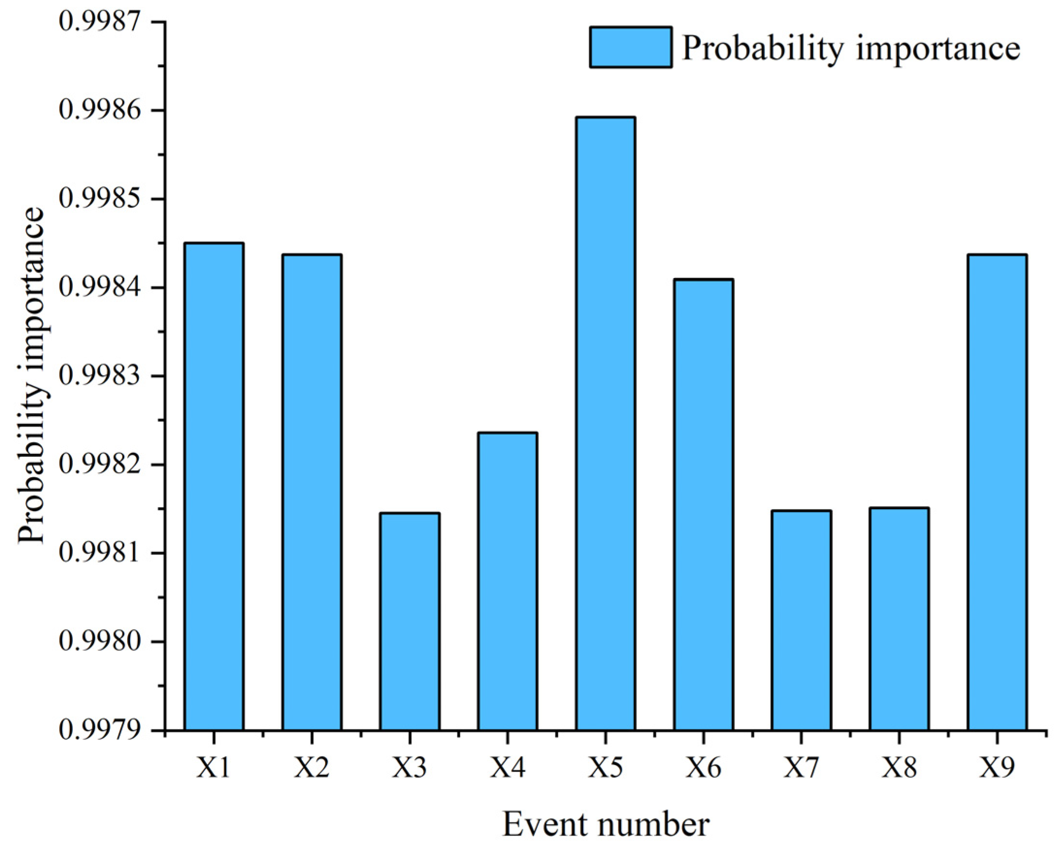
According to the formula and definition, the probability importance and critical probability importance of each bottom event can be calculated as shown in Figure 2 and Figure 3.

Figure 2.
Probability importance of bottom event.
Figure 3.
Bottom event critical probability importance.
3.3. 3D Model Simplification and Construction
The complex structure of a PCB not only includes the substrate, solder pads, solder joints, and electronic components, but also includes the copper foil layer, solder resistance layer, and solder paste layer. If the finite element modeling is carried out blindly according to the actual structure, the workload will be huge and the efficiency of simulation calculation will be reduced. Therefore, it is necessary to simplify the model from the angles of size, function, structure, and material. PCB dual panels are made of spatially isotropic materials with equivalent properties in each layer, such as Young’s modulus, Poisson’s ratio, mass density, etc. [24]. The model can be simplified from the following aspects.
- Size: The substrate and important components are retained, and the influence of the copper foil layer internal wiring, solder resistance layer, and solder paste layer on the model’s structure is ignored.
- Function: The solder joints and solder pads of the important components are retained, and the components are connected to the substrate by pins.
- Structure: Simplify complex structures. The solder joints on the PCB are assumed to be spherical solder joints, and the size of the solder pads is the same as that of the solder joints. There are no defects in this treatment.
- Material: The substrate is made of epoxy resin and glass fiber.
After the structural simplification is complete, a “contact connection” operation is required to build the complete finite element physical models of key substructures and important components. There are several contact connection types available in ANSYS Workbench (https://www.ansys.com/products/ansys-workbench, accessed on 7 June 2024). Considering that the solder joint and pads can be slightly separated, but the stress near the contact surface needs to be obtained, the “rough contact connection” type was considered.
The substrate of the control circuit boards is large in weight and volume, so it is identified as the key substructure. The sensitive weak element diode, control chip, and thin film chip inductance near the chip obtained by FMECA and FTA methods were retained, and the finite element model was established by “coarse contact connection”. The remaining components were simplified according to their importance and impact on the overall quality. The size of the model was 80.6 × 100 × 1 mm, and the diameter of the welding ball was 3.4 mm. The specific material parameters are shown in Table 5 below, and the three-dimensional model of the core components of the PCB is simplified in Figure 4.
Table 5.
Material parameters in engineering data.
Figure 4.
Three-dimensional simplified model of PCB.
In the “Hypermesh” module of Ansys Workbench, “Hide All Other Bodies” wass used to hide models other than the solder joints and pins. Next, the sensitive area with precision requirements (rough contact area) was refined: the mesh size was set to 1 mm, and the meshes were divided into hexahedral meshes. In order to improve the efficiency of mesh optimization, the rest were divided into tetrahedral meshes.
4. Modal Analysis and Random Vibration Analysis
4.1. Modal Calculation
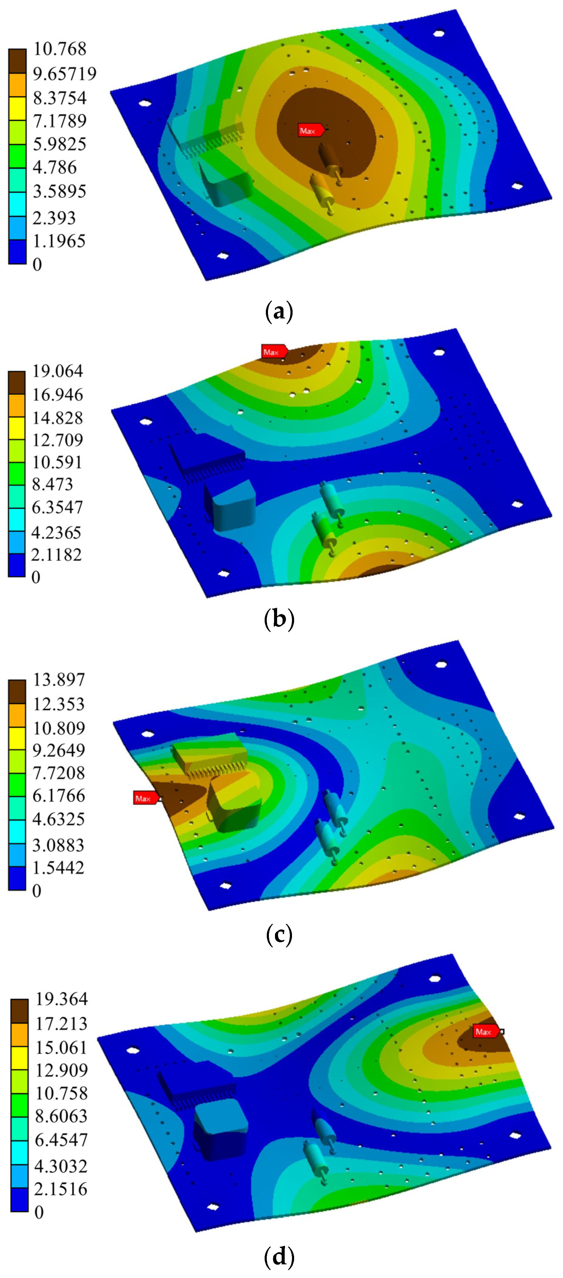
In this paper, the structural characteristics of the system were obtained via modal analysis, and its natural frequency and mode were obtained. The modal optimization was realized by changing the natural frequency of the product. The default Block Lanczos method of ANSYS was used to analyze the mode of the PCB with constraints, which provided accurate modal solutions for the following random vibration analysis and optimization. The frequency range of this analysis was set to be 0~1000 Hz, and the first four mode shapes were analyzed. According to the actual constraints, fixed constraints were added to the four positions A, B, C, and D in Figure 4. The first four mode shapes are shown in Figure 5, and the first four vibration frequencies are shown in Table 6.

Figure 5.
Diagram of the first four mode shapes. (a) The center of the substrate is transverse bent; (b) Both sides of the substrate are transverse bent; (c) Lateral substrate bending twist; (d) The other side of the substrate is bent and twisted.
Table 6.
Calculation mode results of the board.
According to the mode shape diagram, the first two orders of mode shapes are dominated by single bending deformation. As the order increases, the combined deformation of bending and torsion begins to appear. Under different order modes, it can be seen that the maximum deformation occurs at different locations, which indicates that there are multiple structural weaknesses in the substrate and important components. In the first mode response, the substrate was in a center-symmetric bending state, and the capacitor near the midline is most affected and prone to failure. The maximum amplitude (marked Max in Figure 5) is near the pin and solder joint. In the high-order modal response, the four corners of the substrate gradually warped, and the maximum stress was more concentrated on each side of the substrate. Since the maximum stress point is close to the chip inductor and chip component, this can lead to chip inductor and chip failure. In the reliability optimization of the PCB, the performance and position of the core components that are susceptible to interference should be considered, such as diodes, chip inductors, and chips, as well as the welding quality of the solder joints. The following methods can avoid the occurrence of mechanical resonance when the PCB is working.
Method 1: The staggered degree between the natural vibration frequency and vibration source frequency is greater than 20%, which can avoid resonance [25]. The equation for calculating the staggered degree of each mode frequency is as follows:
In order to avoid a Stagger degree of less than 20%, the frequency isolation device can be used to reduce the influence of the PCB by the external excitation frequency.
Method 2: Change the method of fixing the supports, or increase the number of fixed supports to improve the natural frequency of the PCB and avoid mechanical resonance.
4.2. Modal Test
There are multiple sources of errors in the simulation process, including model error, material attribute error, mesh density error, etc. [26]. If there is a big difference between the modal test results and the simulation results, the simplified model needs to be modified to ensure the reliability and accuracy of the simulation results. The natural frequency of the modal test object is high in this paper, so the influence of gravity can be ignored.
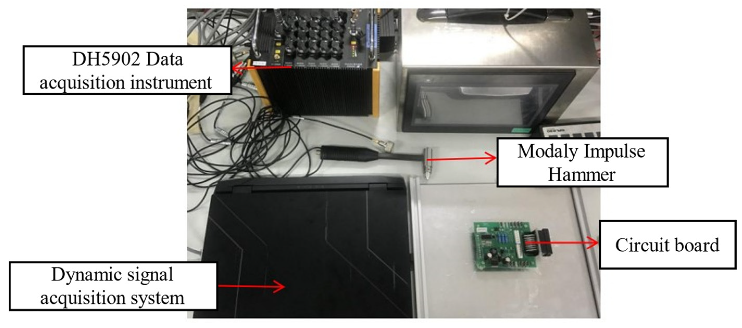
The modal test equipment included a DHDAS dynamic signal acquisition and analysis system, force hammer, ICP-type acceleration sensor, and DH5902N data acquisition instrument. The test method was a single-point vibration pickup force measurement. Firstly, a force hammer was used to strike the excitation points near the measuring points to generate pulse excitation, and the response of the excitation points was measured by the acceleration sensors. After the frequency response function between the force measurement point and the response point was obtained, the modal frequency and modal mode of the experimental object were analyzed and calculated. The experimental data obtained through the MAC modal test were compared with the simulation data to verify the accuracy of simulation modeling. The test equipment is shown in Figure 6.
Figure 6.
Test equipment.
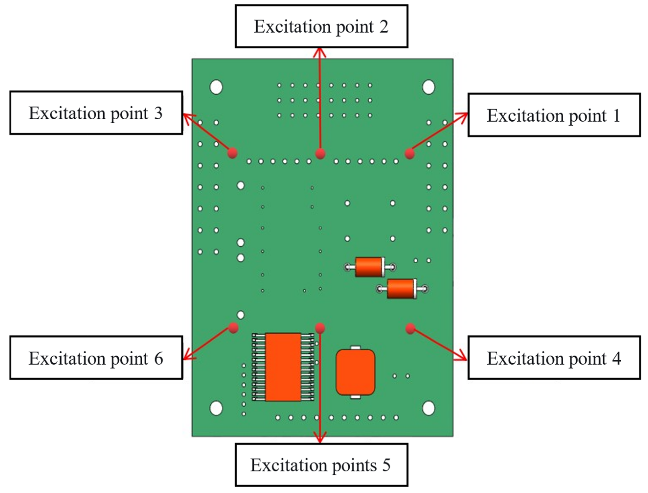
The force hammer and the acceleration sensor were connected to the data acquisition instrument, and the storage mode and basic parameters of the signal were set. The analysis bandwidth was set to 391 Hz; each excitation point was tapped five times to take the average value; and the trigger level of the force hammer channel was set to 10%. After each trigger, you can choose whether to retain it or not to avoid a change in the average times of the counter caused by slight miscontact. The positive direction of the sensor and the force hammer was the Z direction (vertical upward). Because the substrate deformation of the low-order mode was symmetrical at the middle line, the excitation points were set above and below the middle line, close to the position where the vibration was more obvious. The arrangement of the excitation points is shown in Figure 7. The modal test results are shown in Table 7.
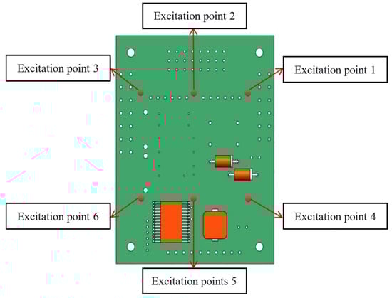
Figure 7.
Incentive point location map.
Table 7.
Test modal results.
It can be seen from Table 3 that the error between the results of the modal test and modal simulation is within 5%, so it can be verified that the reliability of the results of the modal simulation is high. The PCB is likely to be damaged by mechanical resonance when the natural frequency is close to the working excitation frequency in a low-order-mode operating environment. In order to further obtain the weak part of the PCB under the actual working conditions, it was necessary to conduct a random vibration simulation analysis of the model.
4.3. Random Vibration Analysis
The failure of electronic equipment is mostly due to the vibration fatigue caused by broadband random vibrations. With damage caused to the components or solder joints of the equipment, the stability and reliability of the PCB will be affected. Researchers have proposed many optimization schemes in PCB structure distribution, solder joint quality reliability, and constraint arrangement, but most of them are based on simulation analysis results [27,28,29]. In this paper, combined with the qualitative analysis results of FMECA, random vibration simulation analysis and modal analysis were used to verify weak parts, which provides a theoretical basis for reliability optimization design.
Using the frequency response function and modal superposition technique, the absolute value of the mean square response of the i-order free displacement under a weakly damped condition can be obtained as [30,31]:
where is the dynamic range of the self-spectral density function, is the quasi-static part of the self-spectral density function, and is the cross-spectral density function of the static and dynamic degrees of freedom. represents the real part of the entry.
Through random vibration analysis, the corresponding displacement solution and stress solution under a certain power spectral density can be obtained. These solutions can be expressed as probability solutions under the category of statistics, which can be divided into 1σ, 2σ and 3σ.
The module of random vibration in ANSYS was used to simulate the random vibration of the PCB, and its constraint was consistent with the modal analysis. The frequency range of the acceleration power spectral density was set from 1 to 350 Hz, and the excitation direction was perpendicular to the surface of the substrate. In this paper, the first mode frequency and 1σ were used for calculation. The equation is as follows:
where γ is the first-order mode participation coefficient, and is the 1σ unilateral upward displacement response. φ is the maximum mode amplitude of the first-order mode shapes. M represents the generalized mass, PSD represents the power spectral density, and f represents the first-order natural frequency.
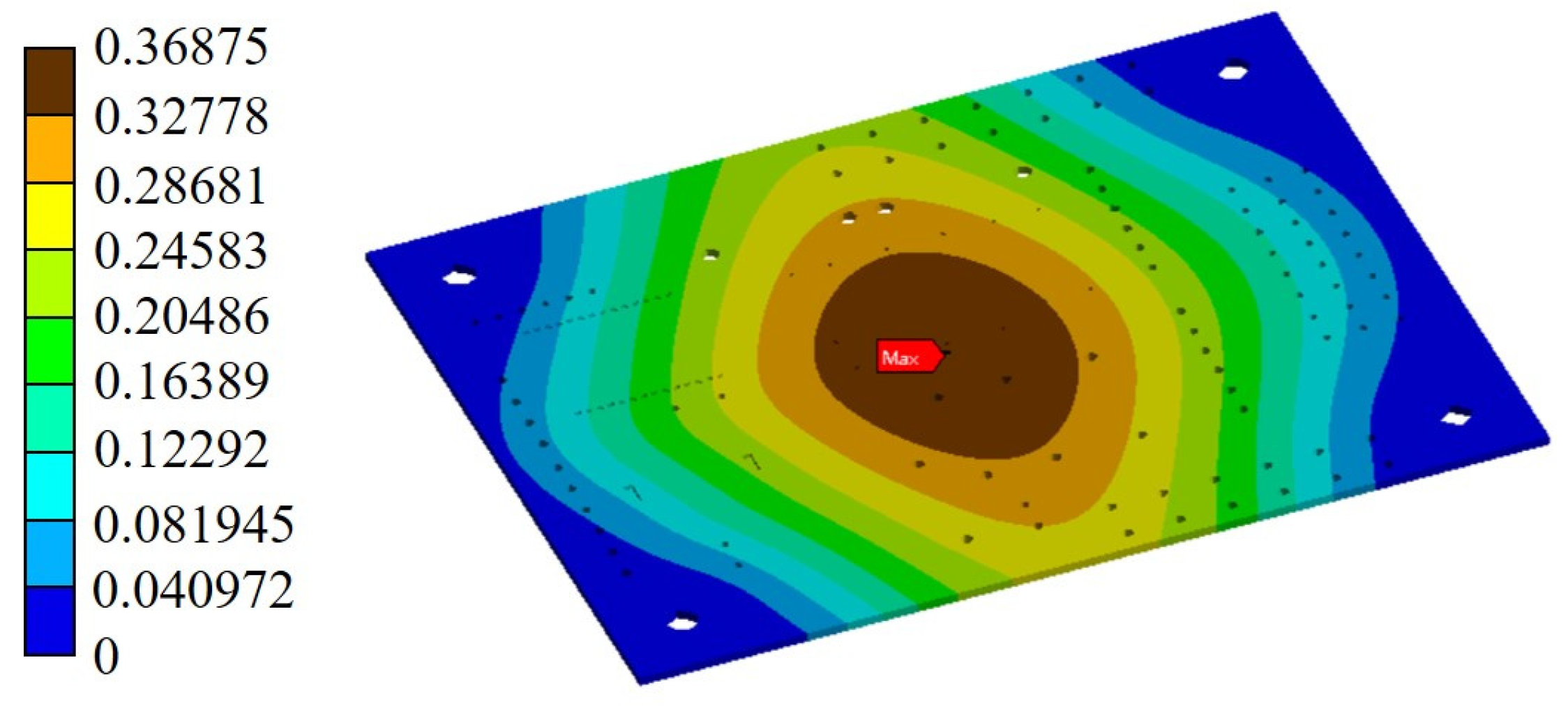
It can be seen from Figure 8 that the response value of the PCB in the first-order mode y direction is 0.36875 mm. The theoretical response value obtained by referring to Equation (15) is 0.313 mm, and the two results are close. Furthermore, Figure 9 shows that at the 1σ solution, the stress is minimal near the center line of the circuit board, and the stress is concentrated near the rigid support points, pins, and through-holes. The maximum stress was found at the second pin solder joint of the main control chip, reaching 2.79 × 10⁷ Pa, and the probability of a 1σ solution was 68.269%. In summary, the random vibration simulation process is reasonable and reliable.
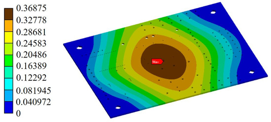
Figure 8.
Response diagram of substrate displacement in the y direction.
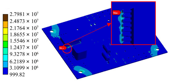
Figure 9.
Stress response graph of PCB under 1σ.
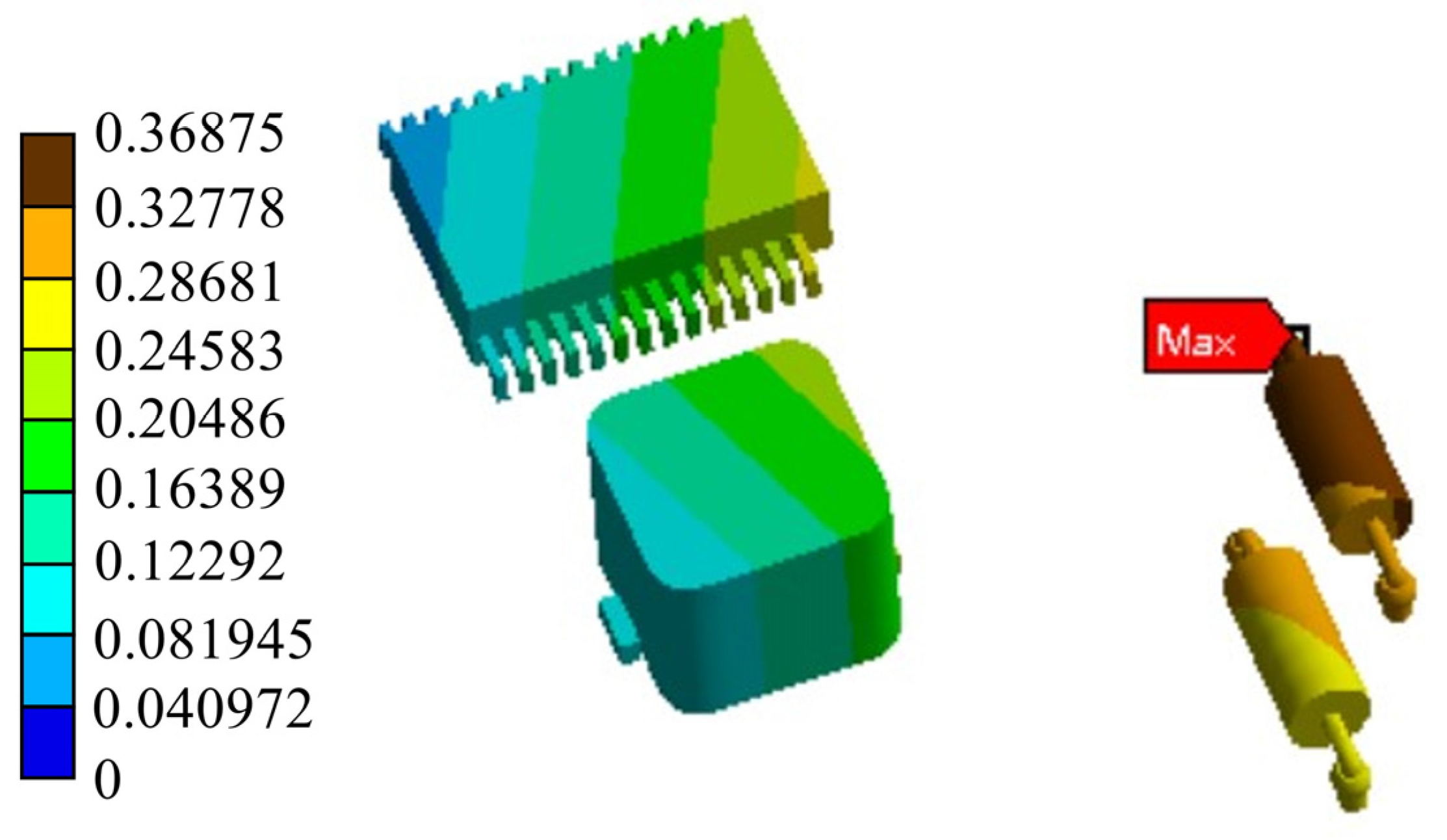
As can be seen from the component vibration response in Figure 10, the maximum vibration response of the diode is located at the joint of the welding ball and the pad. In the actual work process, it is easy for this to be affected by external vibration excitations, resulting in the fatigue damage of materials and structures gradually increasing until failure. The displacement at the center line of the substrate is the largest, and the deformation decreases to both sides, which is consistent with the first-order modal response results obtained from the modal analysis. The capacitive electronic components near the center line are most affected by vibration, so they need to be optimized for solder joints or pins. In addition, materials with higher natural frequencies should also be given priority for the substrate.

Figure 10.
Vibration response diagram of components in the y direction.
4.4. Optimization
In summary, the structural design optimization methods of a drilling rig PCB based on random vibration simulation dynamic analysis are as follows:
- 1.
- Reliability optimization in packaging.
Increase the PCB with a fastening point between components to increase the resistance of the solder joint performance of vibration;
An EC-2216 epoxy adhesive is used to reinforce the device body, which can disperse most of the stress generated by random vibrations of the PCB;
In the actual processing, the height and diameter of the chip welding post can be appropriately increased within the allowable range of process conditions to improve the vibration fatigue reliability of the structure;
The vibration stress response between the pins, solder joints, and pads can be reduced by reasonably controlling the side-length shape parameters.
- 2.
- Reliability optimization of the substrate.
As the key substructure of the PCB, the substrate should have high reliability. The use of a high-frequency plate instead of a low-frequency plate can improve the performance parameters of the material, increasing the low-order-mode frequency. In this way, the occurrence of mechanical vibration fatigue damage can be reduced.
After replacing the low-frequency plate with the FR-4 high-frequency plate, the modal analysis was re-performed. The frequencies of each mode obtained are shown in Table 8. The low mode order of the optimized PCB is much higher than the excitation frequency in the working state, and the resonance phenomenon can be avoided well. In addition, adding an anti-vibration seat or reinforcing bar can also reduce the response of PCB caused by vibration load [32,33].
Table 8.
Calculation modal results.
5. Conclusions
This paper uses ANSYS Workbench to conduct a modal test and a simulation of the control circuit boards in a full hydraulic power head drill; the weak part of the PCB is found, and optimization suggestions are provided for the actual production.
- 1.
- The first four mode frequencies of the PCB are obtained via modal simulation. It is found that in the low-order mode power frequency, the center line of the PCB is easy to bend, and the diodes of nearby important components are most susceptible to failure; at high-order power frequency, the substrate has multiple side stress concentrations, and the chip inductance and chip are prone to failure.
- 2.
- In the simulation of random vibration under actual conditions, the stress displacement cloud and random vibration response diagram can be observed: the diode amplitude is obvious, while the chip inductance and the chip internal stress are large. These results are all consistent with the FMECA.
- 3.
- In the design of the reliability optimization scheme of the PCB, the optimization methods of the core components susceptible to interference in the package and the selection criteria of substrate materials are put forward. These methods can effectively reduce the influence of random vibration stress on the PCB, eliminate the vibration fatigue fracture, improve the vibration reliability of the PCB, and reduce the occurrence of vibration failures.
Author Contributions
J.T.: writing—reviewing and editing; E.S.: validation, writing—original draft; J.Z.: software; X.D. and Y.C.: conceptualization; G.L.: resources. All authors have read and agreed to the published version of the manuscript.
Funding
This research was financially supported by the National Natural Science Foundation of China (52175472; 62302263), the Zhejiang Provincial Natural Science Foundation of China (LD24E050011; LGG22E050031; ZCLTGS24E0601), the Natural Science Foundation of Zhejiang Province for Distin-guished Young Scholars (LR22E050002), the Science and Technology Plan Project of Quzhou (2021F010; 2022K90; 2021K41), and the National College Students’ Innovation and Entrepreneurship Training Program of China (202311488011).
Data Availability Statement
The data that support the findings of this study are openly available at https://github.com/EnyuShi759/MODAL.git (accessed on 5 June 2024).
Conflicts of Interest
Author Guohua Li was employed by the Quzhou Hixee Electronic Technology Co., Ltd. The remaining authors declare that the research was conducted in the absence of any commercial or financial relationships that could be construed as a potential conflict of interest. The Quzhou Hixee Electronic Technology Co., Ltd. had no role in the design of the study; in the collection, analyses, or interpretation of data; in the writing of the manuscript, or in the decision to publish the results.
References
- Jung, D.; Sharma, A.; Jung, J. A review of soft errors and the low α-solder bumping process in 3-D packaging technology. J. Mater. Sci. 2018, 53, 47–65. [Google Scholar] [CrossRef]
- Muhammad, N.; Fang, Z.; Shoaib, M. Remaining useful life (RUL) estimation of electronic solder joints in rugged environment under random vibration. Microelectron. Reliab. 2020, 107, 113614. [Google Scholar] [CrossRef]
- Tian, R.; Wang, C.; Tian, Y.; Zhao, L. Life prediction of CBGA soldered joints under extreme temperature thermal shock. Trans. China Weld. Inst. 2017, 38, 93–97. [Google Scholar]
- Kaya, G. A Novel Hybrid Optical Imaging Sensor for Early Stage Short-Circuit Fault Diagnosis in Printed Circuit Boards. Trait. Signal 2024, 41, 531–542. [Google Scholar] [CrossRef]
- Doranga, S.; Schuldt, M.; Khanal, M. Effect of Stiffening the Printed Circuit Board in the Fatigue Life of the Solder Joint. Materials 2022, 15, 6208. [Google Scholar] [CrossRef]
- Li, L.; Jing, B.; Hu, J. Study on Establishing Degradation Model of Chip Solder Joint Material under Coupled Stress. Materials 2020, 13, 1813. [Google Scholar] [CrossRef] [PubMed]
- Yamamoto, M.; Shohji, I.; Kobayashi, T.; Mitsui, K.; Watanabe, H. Effect of Small Amount of Ni Addition on Microstructure and Fatigue Properties of Sn-Sb-Ag Lead-Free Solder. Materials 2021, 14, 3799. [Google Scholar] [CrossRef]
- Li, C.; Yan, Y.; Gao, T.; Xu, G. The influence of Ag on the microstructure, thermal properties and mechanical behavior of Sn–25Sb-xAg high temperature lead-free solder. Vacuum 2021, 185, 110015. [Google Scholar] [CrossRef]
- Wang, F.; Yue, Z.; Liu, J.; Qi, H.; Sun, W.; Chen, M.; Wang, Y.; Yue, H. Quantitative imaging of printed circuit board (PCB) delamination defects using laser-induced ultrasound scanning imaging. J. Appl. Phys. 2022, 131, 053101. [Google Scholar] [CrossRef]
- Karthiheyan, S.; Verma, V.; Saravanan, S.; Ayyappan, V.P.; Sathiyaseelan, K.; Gopinath, U. Dynamic Response Characteristics and Fatigue Life Prediction of Printed Circuit Boards for Random Vibration Environments. J. Fail. Anal. Prev. 2020, 20, 920–929. [Google Scholar] [CrossRef]
- Sa, Z.; Wang, S.; Fen, Y.; Ma, J.; Zhang, N.; Yu, G.; Liang, J.; Tian, Y. Simulation of SiP Solder Joint Geometry and Random Vibration Reliability Prediction. J. Mech. Eng. 2022, 58, 276–283. [Google Scholar]
- Longteng, L.; Bo, J.; Jiaxing, H. The degradation study for QFP interconnection structure based on PCMD health index and Darveaux model. Microelectron. Reliab. 2020, 109, 113662. [Google Scholar] [CrossRef]
- Chu, L.; Zhou, P.; Shi, J.; Braun, R. Sensitivity analysis for geometrical parameters of BGA in flip-chip packaging under random shear stress and thermal temperature. IEEE Trans. Compon. Packag. Manuf. Technol. 2021, 11, 765–777. [Google Scholar] [CrossRef]
- Yu, S.; Dai, J.; Li, J. Research on the Reliability of Interconnected Solder Joints of Copper Pillars under Random Vibration. J. Electron. Test. 2024, 40, 107–116. [Google Scholar] [CrossRef]
- Samavatian, V.; Masoumian, A.; Mafi, M.; Lakzaei, M.; Ghaderi, D. Influence of directional random vibration on the fatigue life of solder joints in a power module. IEEE Trans. Compon. Packag. Manuf. Technol. 2018, 9, 262–268. [Google Scholar] [CrossRef]
- Catelani, M.; Ciani, L.; Venzi, M. Failure modes, mechanisms and effect analysis on temperature redundant sensor stage. Reliab. Eng. Syst. Saf. 2018, 180, 425–433. [Google Scholar] [CrossRef]
- Ciani, L.; Guidi, G.; Patrizi, G. A critical comparison of alternative risk priority numbers in failure modes, effects, and criticality analysis. IEEE Access 2019, 7, 92398–92409. [Google Scholar] [CrossRef]
- Fan, J.; Zhang, L.; Liu, H.; Pan, R. Reliability Analysis for Numerical Control System of Numerical Control Grinder Based on FMECA and FTA. Mach. Tool Hydraul. 2022, 50, 188–191. [Google Scholar]
- Gao, G.; Zhou, L. Fault Tree Analysis on Reliability of Electronic Control System of Adaptive Optics. Laser Optoelectron. Prog. 2016, 53, 010102. [Google Scholar]
- Lambert, H. Fault Trees for Decision Making in Systems Analysis; University of California: Livermore, CA, USA, 1975. [Google Scholar]
- Rossing, T.D. Modal Analysis; Springer Handbook of Acoustics; Springer: New York, NY, USA, 2007; pp. 1165–1177. [Google Scholar]
- Feng, Y.; He, B.; Rui, X.; Cui, J.; Li, S. Analysis of Vibration Characteristics of Periodic Structure Based on Modal Synthesis Transfer Matrix Method. In International Conference on Mechanical System Dynamics; Springer Nature Singapore: Singapore, 2023; pp. 1355–1367. [Google Scholar]
- Khoo, L.; Mantena, P.; Jadhav, P. Structural damage assessment using vibration modal analysis. Struct. Health Monit. 2004, 3, 177–194. [Google Scholar] [CrossRef]
- Somashekar, V.; Harikrishnan, S.; Ahmed, P.; Ahmed, P.S.A.; Kamesh, D. Vibration response prediction of the printed circuit boards using experimentally validated finite element model. Procedia Eng. 2016, 144, 576–583. [Google Scholar] [CrossRef]
- Fu, D.; Wang, F.; Zhou, P.; Xiao, R.-F.; Yao, Z.-F. Impact of impeller stagger angles on pressure fluctuation for a double-suction centrifugal pump. Chin. J. Mech. Eng. 2018, 31, 10. [Google Scholar] [CrossRef]
- Anderson, A.; Ellis, B.; Weiss, J. Verification, validation and sensitivity studies in computational biomechanics. Comput. Methods Biomech. Biomed. Eng. 2007, 10, 171–184. [Google Scholar] [CrossRef]
- Yang, Y.; Ye, S.; You, S.; Xu, G. Plug-in PCB built-in Vibration reduction Design Method and its PSD Dynamic Simulation. Vib. Shock 2007, 26, 39–42. [Google Scholar]
- Luo, D.; Zhao, Y.; Wang, Z.; Li, G. Thermal Layout Optimization of Power Devices on PCB. In International Conference on Wireless Power Transfer; Springer Nature Singapore: Singapore, 2023; pp. 181–188. [Google Scholar]
- Fahri Berk, B.; Erhan, A.; Barış, E.; Çakır, M.C. Investigation of the effect and optimization of material properties on the printed circuit board. Compos. Adv. Mater. 2023, 32, 26349833231209336. [Google Scholar] [CrossRef]
- Sofiane, S.; Sampathkumar, G.; Renan, L. Simulation assessment of solder joint reliability for fully assembled printed circuit boards. Microelectron. Reliab. 2024, 153, 115320. [Google Scholar]
- Xie, C.; Tao, G.; Wen, Z. Dynamic Stress Analysis and Structural Optimization of Braking Pipeline of Metro Vehicle. J. Mech. Eng. 2021, 57, 118–125. [Google Scholar]
- Wang, H.; Peng, X.; Guo, F.; Ding, Y.; Chen, Q. Research on reliability of CCGA reinforcement process for aerospace electronic products. Trans. China Weld. Inst. 2022, 43, 102–107. [Google Scholar]
- Prashanth, M. Vibration analysis of printed circuit boards: Effect of boundary condition. AIP Conf. Proc. 2018, 1943, 020018. [Google Scholar]


Disclaimer/Publisher’s Note: The statements, opinions and data contained in all publications are solely those of the individual author(s) and contributor(s) and not of MDPI and/or the editor(s). MDPI and/or the editor(s) disclaim responsibility for any injury to people or property resulting from any ideas, methods, instructions or products referred to in the content. |
© 2024 by the authors. Licensee MDPI, Basel, Switzerland. This article is an open access article distributed under the terms and conditions of the Creative Commons Attribution (CC BY) license (https://creativecommons.org/licenses/by/4.0/).