Abstract
With the rapid development of the electronic information industry, more and more attention has been paid to piezoelectric ceramic materials, but the electrical properties and characteristics of piezoelectric ceramic materials have problems such as high cost and inconvenient measurement. In this paper, a new method of electroinduced strain measurement of piezoelectric ceramics is proposed, and an innovative measuring device is constructed based on the working mode and testing principle of an optical displacement sensor and piezoelectric ceramics. An optical displacement measuring device with a simple structure, convenient operation, high measurement accuracy, and good cost benefit was designed and manufactured, and the electroinduced strain performance of piezoelectric ceramics was effectively measured. It is verified by experimental analysis that the device can accurately measure the axial displacement of various piezoelectric ceramics, the measurement accuracy is comparable to the existing equipment, the error is less than 10%, and has good stability and repeatability, which provides a reliable technical means for the performance measurement of piezoelectric ceramics.
1. Introduction
In today’s scientific and technological research field, the current situation of piezoelectric ceramic electroinduced strain measuring instruments restricts the in-depth development of related research and teaching work to a certain extent [1,2,3]. Existing such measuring instruments generally have high cost problems, and their complex manufacturing processes, high-precision components, and advanced technology integration make their prices high [4,5]. Not only that, they also tend to have a large size, both in terms of space occupation in the laboratory, and in the transportation and installation of equipment, which has brought a lot of inconvenience. The characteristics of high cost and large size for educational institutions greatly limit its popularization in teaching practice. Educational institutions are usually faced with a limited budget, and it is difficult to bear the cost of purchasing these expensive instruments, so that they can not provide students with enough practical operation opportunities, which is not conducive to students’ in-depth understanding and mastery of piezoelectric ceramics-related knowledge. In terms of research facilities, although the research work has high requirements for measurement accuracy and performance, the high cost also makes many research institutions have to weigh carefully in equipment procurement. Limited funds may be used in the purchase of these measuring instruments, which affects the development of other research projects and the reasonable allocation of research resources. Moreover, large instruments may require dedicated space to house them, which is a practical problem for some research facilities with limited space, limiting their flexible application in different research scenarios. Therefore, there is an urgent need for an innovative solution to break this status quo, in order to meet the needs of educational institutions and research facilities for low-cost, small size, and high precision piezoelectric ceramic electrostrain measurement instruments, and to promote the continuous development of research and teaching in piezoelectric ceramics-related fields. Over the last decade, advancements in high-precision measurement technology, real-time measurement techniques, laser interferometry, grating measurement, and related technologies have led to increased attention on optical measurement technology and its interference characteristics [6,7,8,9].
Optical measurement technology, a high-precision and non-contact measurement method widely used for small displacement measurements, has gained prominence in scientific research, industrial production, medical diagnosis, and other fields [10,11,12]. According to different optical principles, optical measurement technology can be divided into laser triangulation [13], optical lever method [14], grating ruler measurement method [15], fiber displacement measurement method [16], and laser interferometry [17], etc.; the measurement resolution is between tens of picometers to a few nanometers. In addition, X-ray interferometry, which uses the X-ray diffraction effect to measure displacement, has attracted much attention in recent years [18,19]. Its biggest feature is that the atomic spacing in the lattice structure is used as the traceability standard, which can achieve high resolution of picometer order and avoid various nonlinear errors of optical interferometers [20,21]. Additionally, optical measurement techniques are also applied in various research fields. For instance, Wang et al. provided a systematic review of surface contour measurement techniques using optical interference measurement and classified them in detail according to their working principles [22]. Joo et al. introduced several optical techniques and their latest advancements used in film metrology, reflecting the technological trends in thin film metrology [23]. In the automotive sector, Winter et al. proposed a comprehensive approach for achieving high-precision determination of the relative permittivity of multilayer automotive coatings for radar operating frequency determination [24]. Of course, optical measurement techniques are predominantly applied in surface measurement [25,26] and displacement measurement fields [27]. In addition, there are many presentations of optical measurement in other real-time applications. For example, in the field of marine surveying, the off-axis four-reflection optical structure proposed by Zhou et al. was used in light single-band sounding lidar, demonstrating the application of optical surveying in marine terrain detection [28]. In the field of materials science, Xue et al. printed BT/HA nanocomposite ceramic scaffolders using digital light processing (DLP) in 2024, demonstrating the role of optical technology in the preparation of advanced materials [29]. In terms of material property prediction, Sun et al. used machine learning to predict the high-temperature ablative resistance of ceramic coatings, which also involved the process of obtaining data by optical measurement technology [30]. These examples demonstrate the diversity and importance of optical measurement techniques in different fields, and provide a broader technical background for the application of optical displacement measurement devices in piezoelectric ceramics strain detection in this study.
At present, the measurement of electrical properties and characteristics of piezoelectric ceramic materials faces many challenges, such as high cost and inconvenient measurement. Traditional measurement methods have some limitations in accuracy, non-contact, equipment cost, and operational complexity. For example, some methods may require a complex sample preparation process, or the measurement environment is demanding, resulting in the accuracy and repeatability of the measurement results. Although the optical measurement technology has the advantages of high precision and non-contact, it still needs to solve problems such as the adaptability of the sensor to the sample and the stability of the measurement system when applied to the strain detection of piezoelectric ceramics. In this study, a new method based on optical displacement measurement is proposed to overcome these problems and improve the efficiency and accuracy of strain detection of piezoelectric ceramics.
The optical displacement measuring device, designed based on optical measurement principles, is a micro-displacement measuring instrument. A micro-displacement device amplifies minute movements either directly or indirectly through micro-structural levers under external influences such as forces, electric fields, or magnetic fields to achieve precise positioning. For instance, micro-displacement creep arises from the inverse piezoelectric effect of piezoelectric ceramics and is controlled via voltage [31]. Utilizing electrostriction or magnetostriction principles, an external electromagnetic field induces micron and nano displacement positioning, characterized by linear and stable expansion under specific loads. Such micro-displacement devices find applications in various fields including cell injection, optical precision focusing, fiber coupling, precision computer numerical control (CNC) machine tools, large-scale integrated circuit manufacturing, precise optical measurements, among others, demonstrating wide-ranging needs and practical utility. Advancements in optical measurement devices continue to evolve. Gao et al. provide a comprehensive summary of precision measurement technologies, outlining the current status of key technologies within precision displacement measurement systems based on gratings, and conducting a comparative analysis of several leading measurement methodologies [15]. Yu et al. devised a real-time three-axis micro-vibration measurement system for assessing micro-vibrations in vibration-sensitive environments, addressing the challenges faced by semiconductor production and testing equipment significantly affected by environmental micro-vibrations [32]. The endeavors of these researchers have significantly contributed to the advancement of optical measurement instrumentation.
Simultaneously, spurred by advancements in materials science, piezoelectric ceramics have emerged as a prominent research focus in recent years. Various performance testing instruments such as ferroelectric analyzers have been developed to evaluate the electrical properties of piezoelectric materials. In the 1950s, American scientist Thomas Davidson’s invention of the laser interferometer marked a significant milestone in the evolution of modern optical measuring devices. Subsequently, a range of precision instruments including laser rangefinders, laser interferometers, and optical projectors have been introduced, finding widespread applications in engineering, manufacturing, scientific research, and other domains. Within scientific investigations, optical measurement techniques are employed in disciplines such as materials science, biomedicine, and astronomy [33,34,35]. Driven by the continuous enhancements in optical instruments and technology, optical measurement technology is increasingly integrated into engineering, scientific, and medical practices. It is anticipated that optical measurement technology will assume an even greater role in future developments, making substantial contributions to human progress and advancements. However, the high cost and large size of instruments used in electroinduced strain measurement of piezoelectric ceramic materials pose challenges by escalating testing expenses for educational institutions and research facilities. Based on the principle of optical measurement, the optical displacement measuring device has the advantages of high precision and non-contact, etc. Through careful design and optimization of various components, such as selecting specific optical fiber displacement sensors, high voltage amplifiers, and data acquisition cards, the accurate measurement of electroinduced strain properties of piezoelectric ceramics is realized, which provides an effective technical way for the performance measurement of intelligent piezoelectric ceramics.
Therefore, this paper proposes a low-cost nano-scale optical displacement measurement method. Building upon this method, an optical displacement measurement device is designed and manufactured. The device offers a simple and reliable structure, ease of operation, high measurement accuracy, and cost-effectiveness. Experimental results reveal that the measuring accuracy of this device aligns with that of existing mature equipment, fully meeting the requirements of electroinduced strain measurement in piezoelectric ceramics.
2. Principle of Optical Displacement Measuring Device
2.1. Piezoelectric Effect
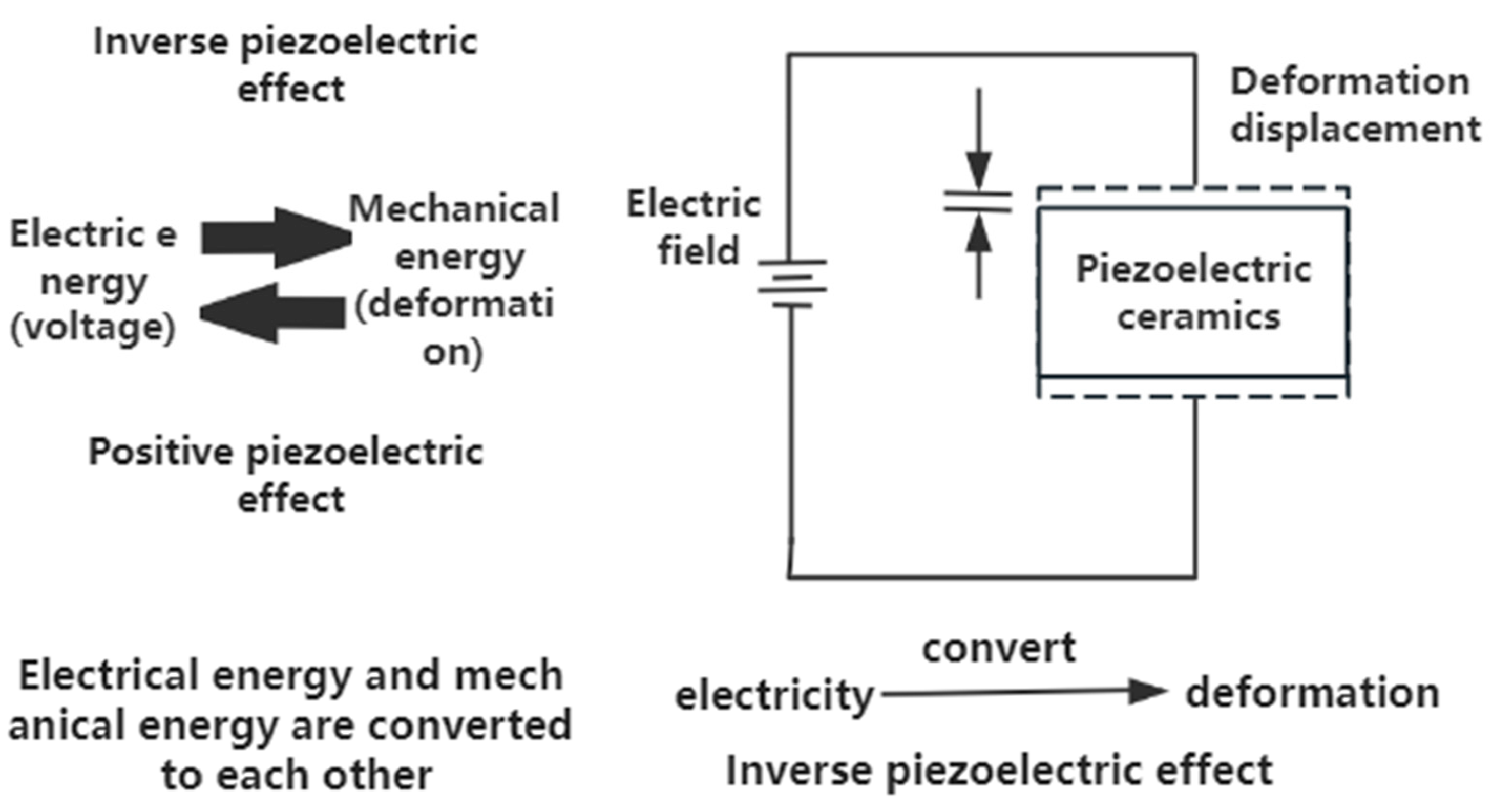
When a dielectric material is subjected to external forces in a specific direction, it exhibits an internal phenomenon of polarization, resulting in the generation of positive and negative charges on its opposing surfaces. Upon removal of the external forces, the material reverts to an uncharged state, a phenomenon known as the positive piezoelectric effect [36]. The polarity of the charges varies accordingly with changes in the direction of the applied force. Conversely, when an electric field is applied in the polarization direction of the dielectric material, it undergoes deformation. Subsequent to the removal of the electric field, the dielectric material returns to its original state, with the deformation dissipating—this phenomenon is termed the inverse piezoelectric effect. The optical displacement measuring device uses the inverse piezoelectric effect of piezoelectric material. This effect occurs when the material, exhibiting piezoelectric properties, deforms proportionally under a specific electric field. Upon removal of the external electric field, the material’s deformation reverts. The positive piezoelectric effect and inverse piezoelectric effect, inversely correlated, collectively characterize the piezoelectric materials’ capability for mutual conversion of mechanical and electrical energy, as depicted in Figure 1.

Figure 1.
Principle of piezoelectric effect.
2.2. Working Principle of Optical Fiber Displacement Sensor
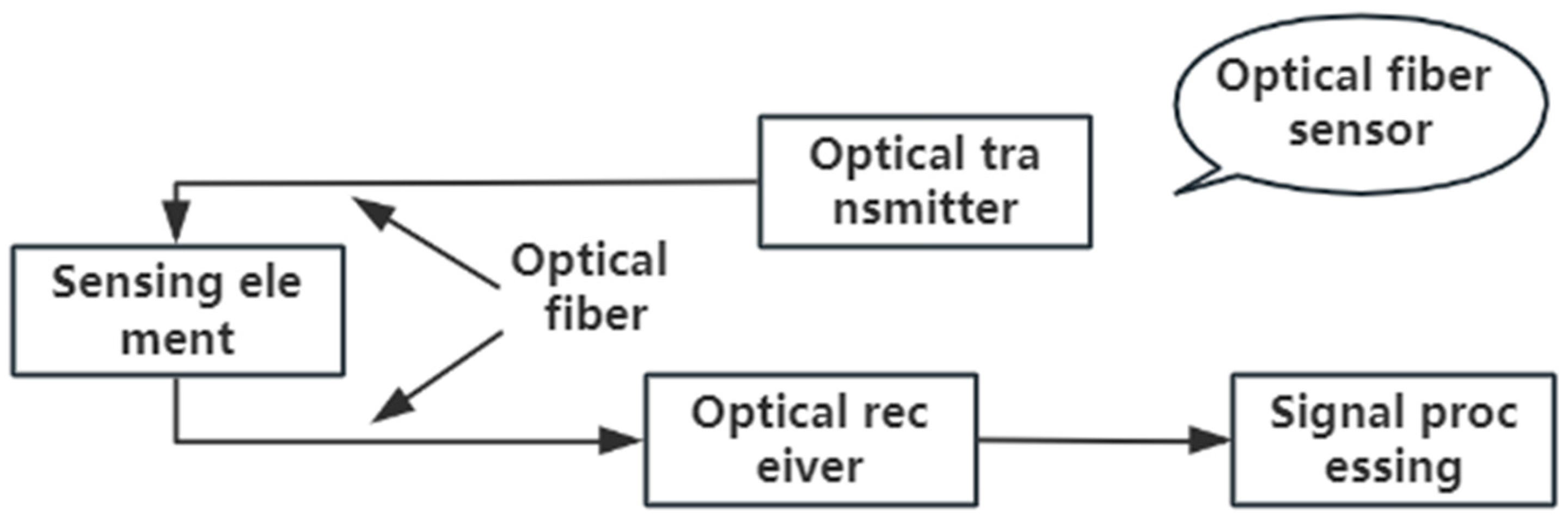
An optical fiber detection system typically comprises an optical fiber waveguide, a laser source, a photodetector, and devices for signal processing, display, and recording, among others. It exhibits a range of characteristics: the dry fiber is small in size, light in weight, and highly pliable, enabling detection in confined areas such as small holes and cracks, with minimal disturbance to the measured field; its excellent insulation and heat resistance render it immune to electromagnetic interference, making it suitable for use in high-temperature, high-voltage environments and various challenging industrial conditions. The fiber optic sensor is highly sensitive, has a broad dynamic range, facilitates remote measurement and control, and can be integrated with computers for intelligent operation.
When the object being measured undergoes a slight displacement, the optical fiber bends slightly, altering the propagation path of the optical signal, and, consequently, the intensity of the optical signal. The photodetector converts these optical changes into electrical signals, which are then processed and analyzed by the signal processing circuit to obtain displacement information of the object. The working principle of the optical fiber displacement sensor is illustrated in Figure 2.
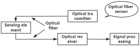
Figure 2.
Working principle of optical fiber sensor.
When the measurement object of the optical fiber displacement sensor is displaced, the optical fiber bending causes the propagation path of the optical signal to change, and the optical signal intensity to change. This process can be explained by the propagation theory of light. According to the law of refraction of light, there is a specific relationship between the angle of incidence and the angle of refraction when light passes from one medium to another. In the fiber, the light propagates along the fiber core, and when the fiber is bent, the incidence angle of the light at the bend changes, resulting in a corresponding change in the refraction angle, and some light may leak from the fiber core to the cladding, thus weakening the intensity of the light signal propagated to the detector. From the perspective of energy conservation of light, the total energy of the optical signal remains unchanged during propagation, but due to the change of the propagation path, the distribution of light in the fiber changes, resulting in a decrease in the light intensity received by the detector. We can use a simple formula to approximate this relationship: if the initial optical signal strength is , the loss coefficient caused by fiber bending is ( related to the degree of fiber bending, fiber material characteristics, and other factors), then the changed optical signal strength can be expressed as , where is the optical path change caused by fiber bending. This formula shows that with the increase in optical path variation (that is, the degree of fiber bending increases), the optical signal intensity decreases exponentially, which intuitively reflects the quantitative relationship between the change in the optical signal propagation path caused by fiber bending and the change in optical signal intensity, providing a strong theoretical support for the relevant statements in this paper.
2.3. Working Principle of Optical Displacement Measuring Device
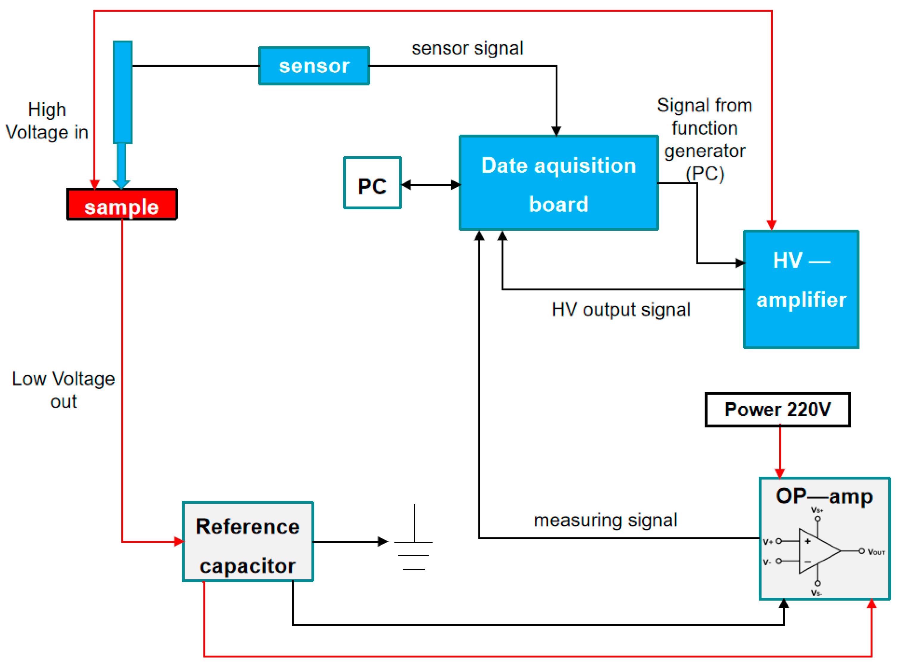
The optical displacement measuring device primarily consists of an optical displacement tester, high voltage amplifier, temperature control device, and a signal acquisition and processing system. The main equipment includes a high voltage amplifier, optical displacement tester, reference capacitor, operational amplifier, temperature controller, optical fiber displacement sensor, thermocouple, data acquisition card, and a computer.
The test method flow is illustrated in Figure 3. The sample is placed on the sample table, and the high-voltage amplifier applies an electric field to the sample via the high-voltage input of the sample table and the low-voltage output of the thimble. The thimble is connected to the optical fiber displacement sensor, which is then connected to the acquisition card, facilitating the transmission of the sensor signal to the computer for processing. The reference capacitor is connected to the operational amplifier, which in turn is connected to the acquisition card, enabling the transmission of the polarization measurement signal to the computer for processing. The high voltage amplifier sends the high voltage output signal to the computer, which then feeds back to the high voltage amplifier through the signal generator to adjust frequency, electric field, and other parameters.

Figure 3.
Test method flow chart.
3. Device Design and Manufacture
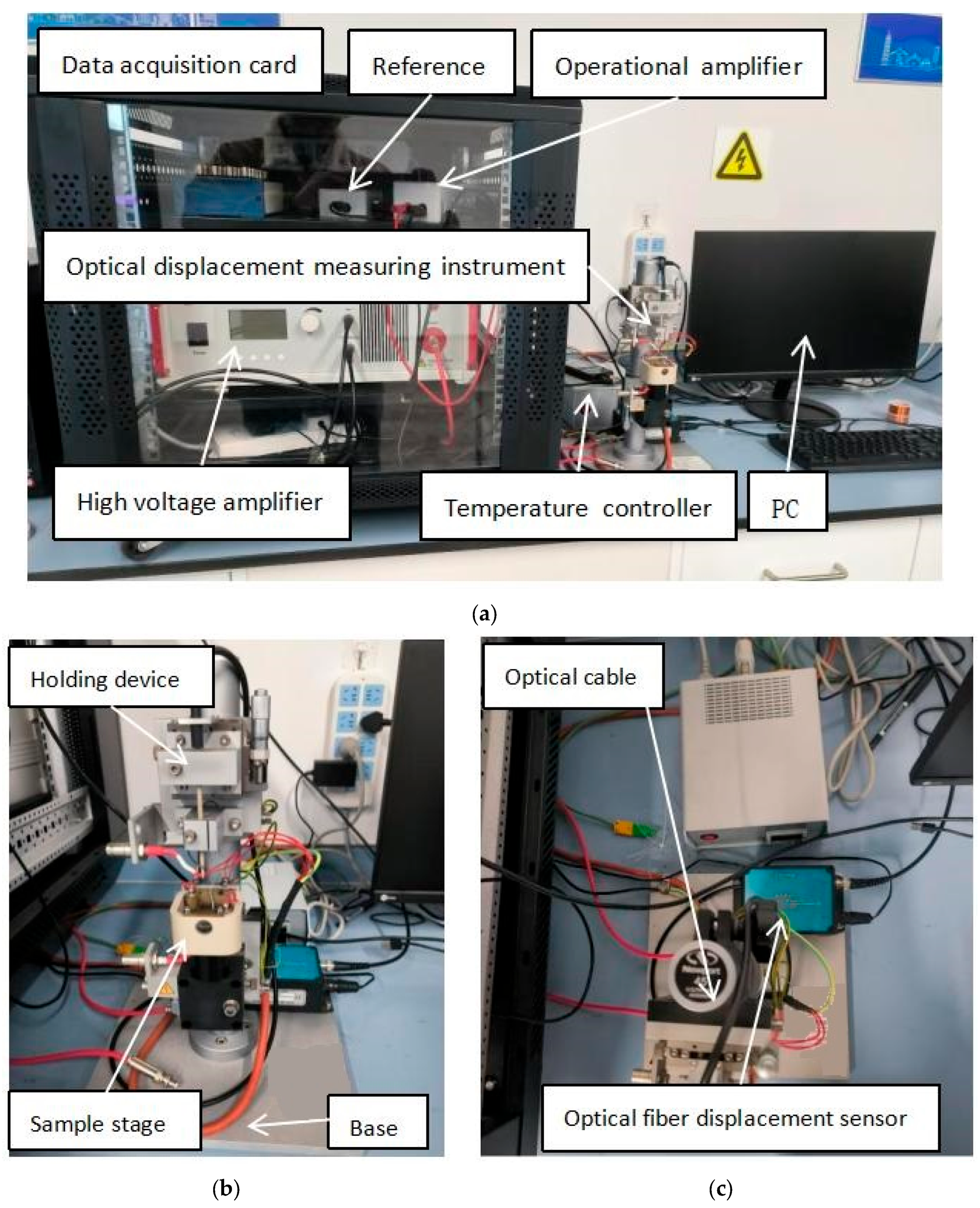
Figure 4a is the overall drawings of the optical displacement measuring instrument, Figure 4b is the main view, and Figure 4c is the top view. The design of the device primarily focuses on the optical displacement measuring instrument, the selection of the optical fiber displacement sensor, high-voltage amplifier, and data acquisition card.

Figure 4.
Optical displacement measuring instrument: (a) overall drawings; (b) main view; (c) top view.
3.1. Optical Displacement Measuring Instrument
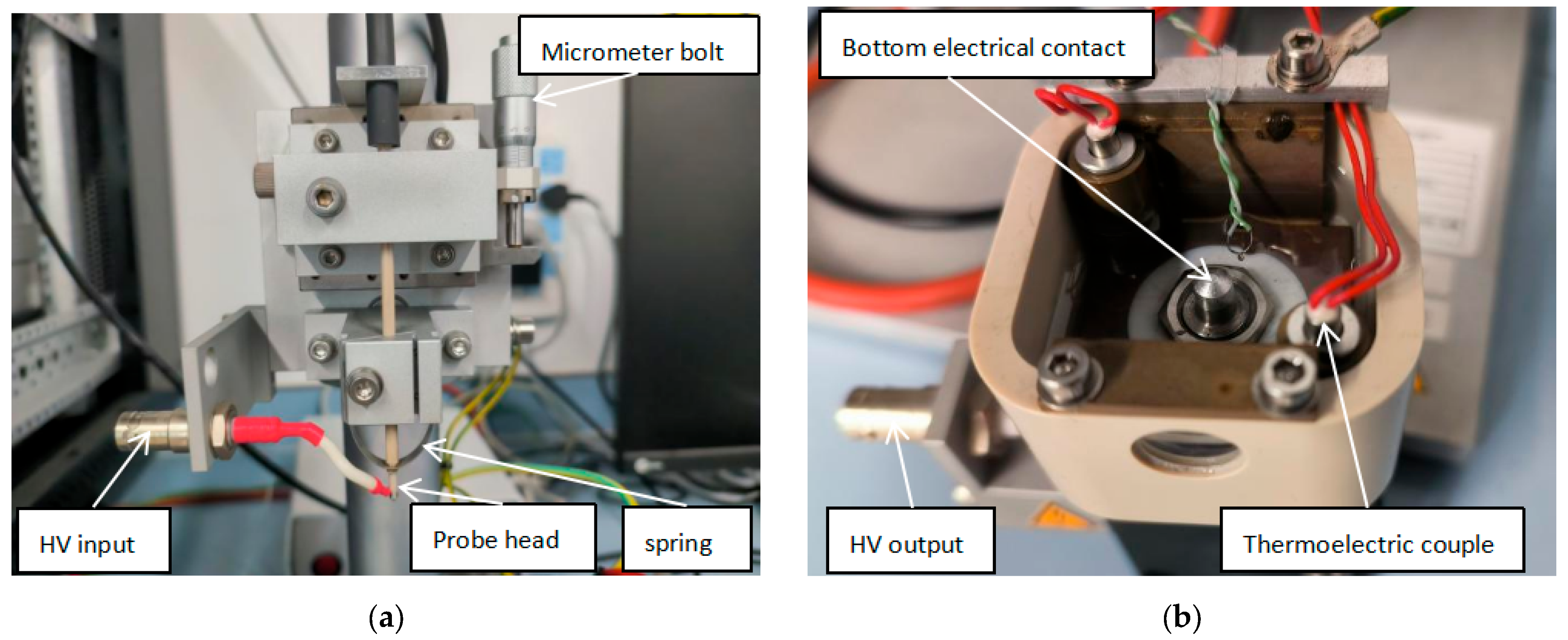
When the optical fiber displacement sensor is used for measuring electroinduced strain via the piezoelectric effect, it is essential to align the sensor’s probe head and the sample’s center on the same straight line. This alignment necessitates specific coaxiality and parallelism between the probe head and the sample center, and also requires maintaining the stability of the clamping force when the sample is secured. The clamping device and sample table designed in this study are adequate for the measurement needs of piezoelectric ceramic materials. Additionally, a spring is incorporated into the clamping device design, providing the probe head with necessary flexibility and ensuring stable clamping force, as shown in Figure 5a. A heating element is included in the sample table design, accommodating the requirements of variable temperature testing for piezoelectric ceramic materials. A high-voltage output connection line is integrated at the bottom of the sample table, enabling the application of an electric field to the sample, as shown in Figure 5b. The optical displacement measuring instrument is entirely made of metal. Compared to acrylic materials, metal offers superior electrical conductivity and greater strength, thus ensuring improved performance while improving the device’s overall weight.
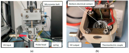
Figure 5.
Optical displacement measuring instrument: (a) physical drawing of the clamping device; (b) physical drawing of the sample table.
3.2. Optical Fiber Displacement Sensor
The optical fiber displacement sensor plays a crucial role in the measurement, enabling the accuracy of piezoelectric ceramic materials to reach the targeted nanometer level. To achieve non-contact, nanoscale accuracy in the measurement process for samples with diameters of 6–15 mm and thicknesses of 0.5–5 mm, the optical fiber displacement sensor is selected as the key component. The device uses the high-precision optical fiber displacement sensor from PHILTEC Company in the United States, Model D63, and its parameters are presented in Table 1. This sensor is a non-contact optical fiber displacement sensor, offering high precision, and resistance to high temperatures and pressures. Additionally, its standard probe structure enables vertical measurements, meeting the requirements for measuring the axial displacement of piezoelectric ceramics.

Table 1.
Parameters of Model D63 optical fiber displacement sensor.
3.3. High Voltage Amplifier and Data Acquisition Card
The high voltage amplifier in the device functions to amplify the input voltage step by step, provide required amplification, establish a high voltage environment for measurement, and offer protection and safety features to prevent unexpected situations such as electric shock and short circuits. The high voltage amplifier model, Aigtek ATA-7030 (Aigtek Electronic Technology Co., Ltd., Xi’an, China), accurately controls voltage gain multiples, drives high voltage loads, and possesses a high single-ended output voltage, making it widely applicable in dielectric field research. For data acquisition, the selected NI USB-6212 BNC (National Instruments Co., Ltd., Austin, TX, USA) data acquisition card maintains high accuracy under a high sampling rate, reducing costs and simplifying signal connections. The device primarily utilizes the high sampling rate and data acquisition functions of this card. Figure 6 illustrates the interface circuit connecting the high voltage amplifier and the data acquisition card.
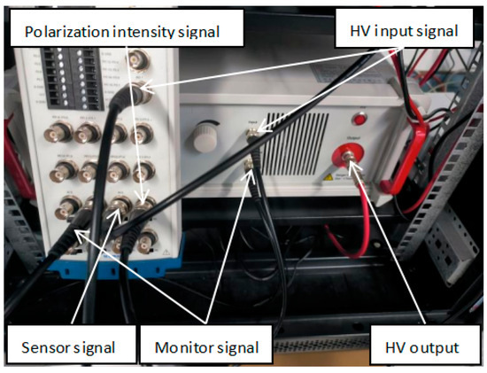
Figure 6.
Schematic diagram of interface circuit.
3.4. Other Components
To monitor the ambient temperature of the sample bench accurately, the Weber temperature controller (Okaylight Electronic Co., Ltd., Dongguan, China) paired with Eurotherm 3216 (Eurotherm Co., Ltd., Worthing, England) is selected. This choice is based on its precise temperature control capabilities and the availability of optional auxiliary functions. The controller is user-friendly, offering various definable input types, as well as features for heater current monitoring and load detection. The selection of reference capacitance is determined by the capacitance of the piezoelectric ceramics. Additionally, the LF356N/NOPB operational amplifier (Xinsihui Technology Co., Ltd., Shenzhen, China) model is employed to handle large capacitive loads without encountering stability issues. This amplifier also provides a wide gain bandwidth, low input noise voltage, internal compensation, and significant differential input voltage capabilities.
3.5. Device Calibration
First, the optical fiber displacement sensor and sample table are precisely adjusted using micrometer bolts. For the sensor, ensure that the probe and the sample center are in the same straight line to achieve the required coaxiality and parallelism requirements to ensure the accuracy of the measurement. For the sample table, its flatness and stability are adjusted so that the sample can be tested on a stable platform. Secondly, the output voltage of the high voltage amplifier is calibrated, and the gain multiple of the amplifier is adjusted by comparison with the standard voltage source to ensure the accuracy of the output voltage. At the same time, the sampling rate, resolution, and other parameters of the data acquisition card are set and calibrated to match the measurement requirements. Throughout the calibration process, tests and adjustments are repeated until the measurement system reaches a stable and accurate state, thus providing a reliable basis for subsequent experimental measurements.
4. Experimental Analysis
4.1. Experimental Setup
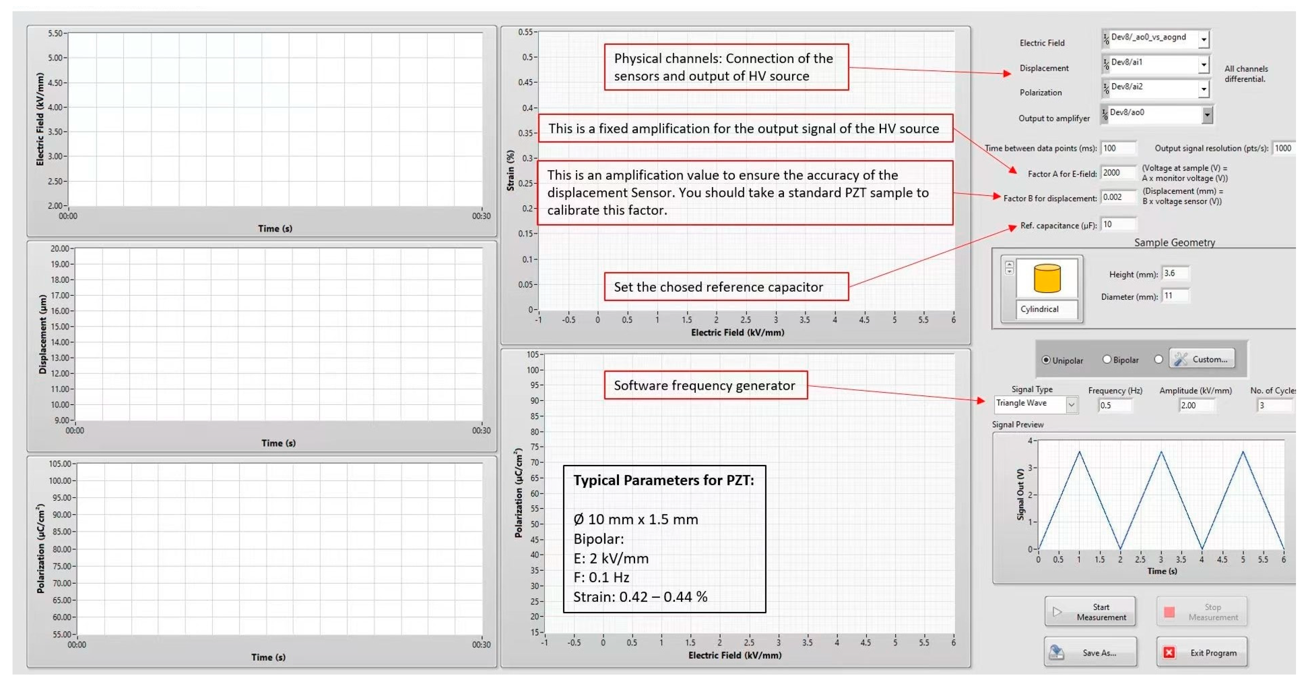
A commercial PIC151 piezoelectric ceramic sample (Yuhai Electronic Ceramics Co., Ltd., Zibo, China) (10 mm in diameter and 1 mm in thickness) was chosen for testing. Prior to conducting measurements with the Axiacct TF 2000 (aixACCT Systems GmbH, Aachen, Germany), the laser was preheated for approximately 20 min. The optical sensor was switched on 15 min before commencing optical displacement measurements. Then, the testing sample was posited at the fixture’s center to measure the electroinduced strain and polarization intensity. The test data panel is illustrated in Figure 7. Several parameters, such as resolution, voltage amplification, and displacement coefficients, were adjusted to ensure the accuracy of displacement measurements.
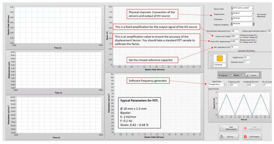
Figure 7.
Test data panel.
Based on the data available, the maximum (or saturation) polarization should be around 36 ± 0.3 C/cm2 at 2 kV/mm in the positive direction and −36 ± 0.3 C/cm2 at −2 kV/mm. The total strain between the maximum and minimum points should be approximately 0.42 ± 0.01%. The second part of the loop should be utilized in the negative electric field. As indicated in Figure 7, the optical displacement measuring device meets the necessary measurement criteria.
4.2. Comparison of Test Accuracy
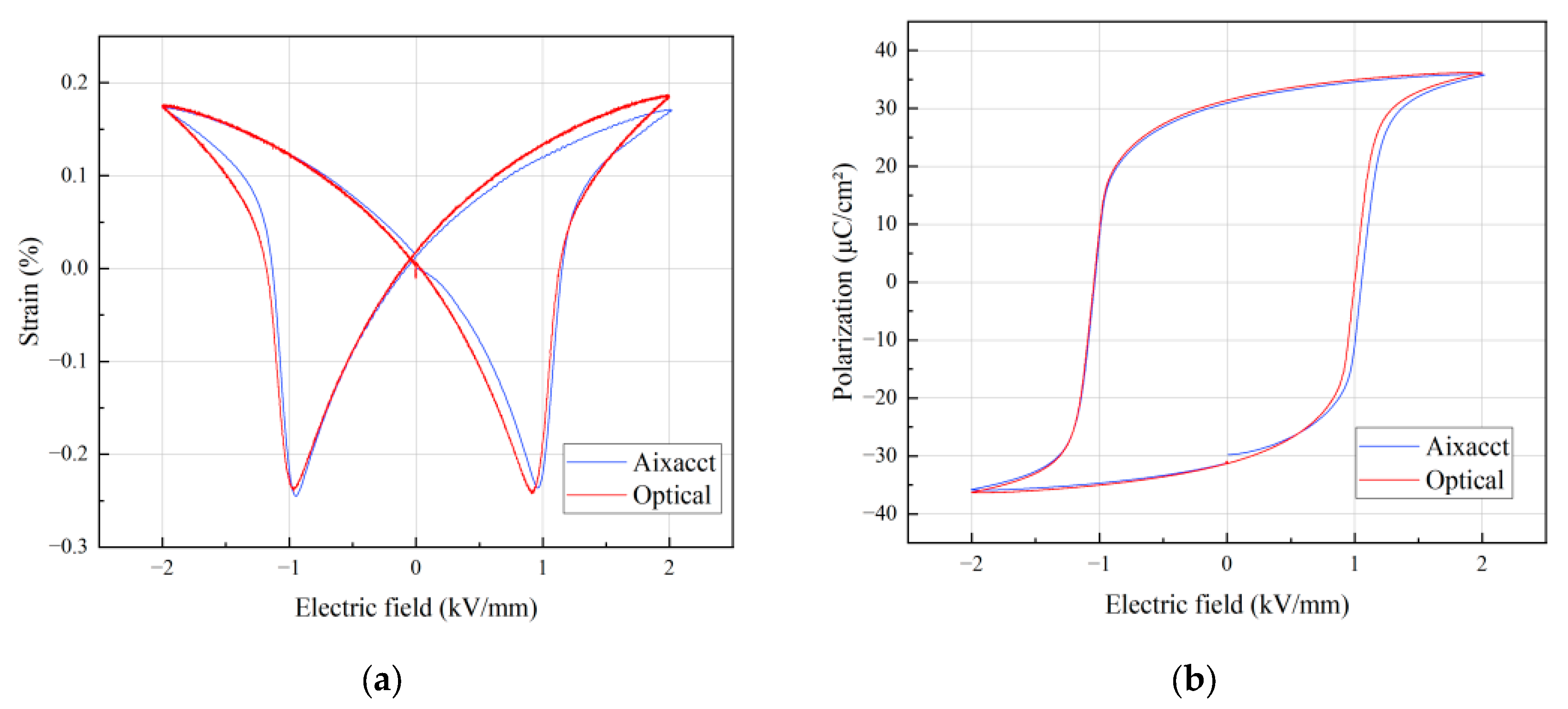
Currently, the laser measuring device in the ferroelectric analyzer is primarily used for assessing the electroinduced strain of piezoelectric ceramics, which in turn reflects the reliability of the optical measurement method from one aspect. Therefore, the optical displacement measuring device developed in this study is used to compare its measuring accuracy with the existing devices in the laboratory. A commercial PIC151 piezoceramic sample with a diameter of 10 mm and a thickness of 1 mm was selected and subjected to five measurement cycles, using both an optical displacement measuring device and a ferroelectric analyzer, under a test electric field of 2 kV/mm. The sensor and sample table were calibrated with a micrometer bolt before the measurements; the measurement results are shown in Table 2 and Figure 8. The maximum positive electroinduced strain and negative electroinduced strain are 0.1732% and 0.2449%, with corresponding polarization values of 36.1385 µC/cm2 and 36.2960 µC/cm2 respectively. The ferroelectric analyzer recorded the maximum positive electroinduced strain of piezoelectric ceramics at 0.1869% and the maximum negative electroinduced strain at 0.2424%, along with the maximum positive polarization of 35.8486 µC/cm2 and the maximum negative polarization of 35.7974 µC/cm2. The maximum positive electroinduced strain error between the two measurement devices is 7.3%, the maximum negative electroinduced strain error is 3.6%, the maximum positive polarization intensity error is 0.8%, and the maximum negative polarization intensity error is 1.39%, all falling within 10%, thus meeting the measurement requirements.
Table 2.
Test accuracy comparison results.
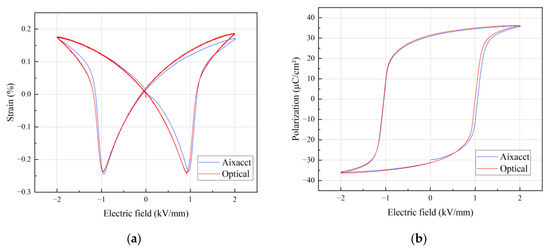
Figure 8.
Measurement results of different devices: (a) result of strain performance; (b) result of polarization performance.
4.3. Repeatability Measurement Experiment
In the repeatability experiment, a new commercial PIC151 piezoelectric ceramic sample, with the same dimensions as the sample tested in the above section (10 mm in diameter and 1 mm in thickness), was selected for testing. The optical displacement measuring device conducted five repeated measurements on the same sample, capturing various positions on its surface to minimize the potential impact of errors on the experimental outcomes. The results, presented in Table 3 and Figure 9, reveal that, through variance analysis, the average maximum positive strain is 0.1627% with a standard deviation of 0.0033. The average maximum negative strain is 0.2197% with a standard deviation of 0.0018. The standard deviation of the device’s measurement results is approximately 0.002, indicating minimal influence of random errors on the measurement outcomes. This suggests that the testing device exhibits good stability and repeatability in the experimental setting.
Table 3.
Repeatability measurement results.
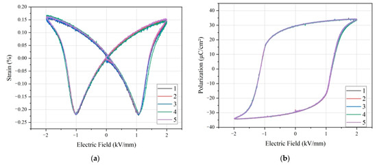
Figure 9.
Repeatability measurement results of the device: (a) result of strain performance; (b) result of polarization performance.
4.4. Brief Summary
Although this study focuses on the strain measurement of piezoelectric ceramics, the method is theoretically scalable and can be applied to some other advanced materials or similar measurement scenarios. For example, the optical displacement measurement method may also be suitable for some materials with piezoelectric characteristics or small displacement changes under the action of an electric field, such as some smart materials, thin film materials, etc. In other application fields, such as the displacement measurement of micro-structures in micro-electro-mechanical systems (MEMS), the detection of tiny deformation of cells or tissues in the biomedical field, etc., as long as the size and displacement change range of the measured object is within the measurement capability of the device, and the measurement principle is consistent, it is possible to use similar measurement methods for research. However, it is important to note that for different materials or application scenarios, the measuring device may need to be properly adjusted and optimized to suit its specific material characteristics and measurement requirements.
It has certain potential to integrate this measurement method with a machine learning algorithm. Machine learning algorithms can analyze and process a large number of measurement data and find the hidden rules and relationships behind the data. For example, by learning the electroinduced strain data of piezoelectric ceramics under different electric field strength, temperature, and other conditions, a prediction model is established to achieve more accurate prediction and optimization of piezoelectric ceramics properties. In addition, machine learning algorithms can also be used for automatic classification of data, anomaly detection, and error correction. For example, by training algorithms to identify different types of measurement error patterns, real-time monitoring and correction of measurement results can improve the accuracy and reliability of measurement. In future studies, we plan to explore combining this measurement method with suitable machine learning algorithms to further improve the research level of piezoelectric ceramic material properties.
In addition, with the continuous development of fiber optic technology, in the future it is expected to have a positive impact on the performance and scalability of this low-cost measurement device. For example, the emergence of new optical fiber materials may further improve the sensitivity and stability of optical fiber displacement sensors, reduce the cost of sensors, and thus improve the performance of the entire measurement device. In optical fiber communication technology, faster data transmission rate and lower signal loss will help achieve more real-time and efficient data acquisition and processing, and enhance the application capability of measurement devices in large-scale data measurement and analysis scenarios. In addition, improvements in optical fiber manufacturing processes may make the structure of optical fiber sensors more miniaturized and integrated, which can be easily deployed in more complex measurement environments, improving the flexibility and scalability of measurement devices. These technological advances will provide a broader development space for the application of fiber-based measurement devices in piezoelectric ceramics strain detection and other related fields.
5. Conclusions
In this experiment, in order to realize the nonlinear contact between the optical fiber displacement sensor and the piezoelectric ceramic sample, we adopted a special sample fixation and sensor installation method. The sample is fixed on the sample table, and the surface of the sample table is specially treated to have a certain roughness to simulate the non-ideal contact conditions that may be encountered in practical applications. The probe of the fiber-optic displacement sensor is mounted above the sample via a fine-tuned bracket that precisely adjusts the distance and angle between the probe and the sample surface. During the initial installation, the probe is adjusted to a position close to the surface of the sample but not in contact, and then the piezoelectric ceramic sample is generated by applying a small electric field. At this time, the sensor output signal is observed, and the fine-tuning bracket enables the sensor to accurately detect the displacement change of the sample, thus establishing a nonlinear contact relationship. Axial displacement refers to the change of displacement of the sample in the direction parallel to the electric field. In the experimental setting, the piezoelectric ceramic sample is placed vertically on the sample table, and the electric field direction is perpendicular to the sample surface, so the displacement along the electric field direction generated by the sample under the action of the electric field is called the axial displacement. In order to accurately measure the axial displacement signal, we arranged a number of optical fiber displacement sensors around the sample table to detect the displacement change of the sample from different angles. Through the comprehensive analysis of the measurement data of multiple sensors, the axial displacement information of the sample can be obtained more accurately. During the experiment, the relevant key parameters that needed to be adjusted include electric field intensity, measurement frequency, and sensor sensitivity. The electric field intensity is precisely controlled by the high voltage amplifier. According to the different measurement requirements, the electric field intensity can be adjusted within a certain range to observe the electroinduced strain characteristics of the piezoelectric ceramics under different electric fields. The measurement frequency determines the time interval of data acquisition. By adjusting the measurement frequency, the measurement accuracy and data acquisition speed can be balanced. For example, the measurement frequency can be increased when the dynamic response characteristics of the sample need to be obtained quickly; when the measurement accuracy is high, the measurement frequency should be appropriately reduced. Sensor sensitivity can be optimized by adjusting the operating parameters of the sensor (such as light source intensity, detector gain, etc.) to ensure that small displacement changes in the sample can be accurately detected. Through reasonable adjustment of these key parameters, more accurate and reliable axial displacement measurement results can be obtained, and the relationship between electroinduced strain properties and electric field of piezoelectric ceramics can be deeply studied.
In this paper, the shortcomings of existing instruments are introduced, and an optical displacement measurement method is proposed. On this basis, an optical displacement measurement device based on the working principle of optical fiber is designed and manufactured. Experimental analysis show that the device is capable of measuring the axial displacement of various PZT (Lead Zirconate Titanate) and KNN (Potassium Sodium Niobate)-based piezoelectric ceramics. Through adjustment of different parameters, the axial displacement of the samples can be measured within the range of 6–15 mm in diameter and 0.5–5 mm in thickness. An analysis of the nonlinear contact between the optical fiber displacement sensor and the piezoelectric ceramic sample is conducted, elucidating the relationship between the axial displacement and the electric field. A comparison of the device’s accuracy with that of the existing measuring device in the laboratory is performed. The results reveal that the measuring error of the device is comparable to that of the laboratory’s measuring device, with errors under 10%. Additionally, the results demonstrate that the test’s standard deviation registers at approximately 0.002, signifying minimal influence of random errors and meeting the requirements of piezoelectric ceramic electroinduced strain measurement. The device has been applied to the measurement of electroinduced strain of piezoelectric ceramics in the laboratory. The results of this study provide a new and effective measurement method for the study of the properties of piezoelectric ceramics. In scientific research, it can help researchers more accurately obtain the electroinduced strain characteristics of piezoelectric ceramics, gain an in-depth understanding of its performance changes under different electric fields, temperatures, and other conditions, and provide data support for further optimization of the performance of piezoelectric ceramics materials. For example, in the development of new piezoelectric ceramic materials, this measurement method can be used to quickly and accurately evaluate the properties of the material and accelerate the development process. In industrial production, piezoelectric ceramics are widely used in sensors, actuators, and other fields. The measurement method can be used for product quality inspection to ensure the consistency and stability of piezoelectric ceramic components in the production process. Through the rapid and accurate performance measurement of products, problems in the production process can be found in time, improve product quality and production efficiency, and reduce production costs.
Author Contributions
Conceptualization and methodology, Y.L., X.H. and Y.Z.; software, J.M. and Z.F.; validation and investigation, J.M. and F.Z.; resources, M.Z. and X.H.; data curation, J.M., Z.F. and F.Z.; writing—original draft preparation, Y.L., J.M. and X.H.; writing—review and editing, M.Z. and Y.Z.; visualization, Z.F. and F.Z.; supervision and project administration, X.H. and Y.Z. All authors have read and agreed to the published version of the manuscript.
Funding
This project and the APC were funded by the Key Science and Technology Plan Project of Jiaxing in China under Grant number 2024BZ20018 and the Research Project of Zhejiang Provincial Department of Education in China (No. Y202454555).
Data Availability Statement
The data will be available by the authors on request.
Conflicts of Interest
Author Zhenhai Fan and Feng Zhang were employed by the company TDG Intelligent Equipment Co., Ltd. The remaining authors declare that the research was conducted in the absence of any commercial or financial relationships that could be construed as a potential conflict of interest.
References
- Tao, C.Y.; Chen, B.J.; Lin, T.; Ma, J.; Dou, Z.S.; Zhang, M.H.; Zhong, M.P.; Gong, W.; Zhou, Y.Q.; Yao, F.Z.; et al. Simultaneously enhanced electrical properties and high-power characteristics of (K,Na)NbO3 lead-free piezoceramics by hot-pressing. Ceram. Int. 2024, 50, 28047–28053. [Google Scholar] [CrossRef]
- Pai, F.S.; Hu, H.L. Driving Circuit Design for Piezo Ceramics Considering Transformer Leakage Inductance. Processes 2023, 11, 247. [Google Scholar] [CrossRef]
- Naldi, C.; Martino, G.; Dongellini, M.; Biserni, C.; Morini, G.L. Experimental analysis of a thermal storage with a PCM-loaded finned heat exchanger. Int. J. Hydromechatron. 2024, 7, 250–263. [Google Scholar] [CrossRef]
- Tao, C.Y.; Xiong, Y.S.; Zhong, M.P.; Wang, G.H.; Zhou, Y.Q. Development of a High-Power Testing System for Piezoelectric Ceramic Material. Meas. Sci. Technol. 2024, 35, 126003. [Google Scholar] [CrossRef]
- Lin, T.; Zhong, M.P.; Wang, G.H.; Zhou, Y.Q. A simple measurement method for in-situ temperature-dependent piezoelectric coefficient d33 of piezoelectric materials. Eng. Res. Express 2024, 6, 025561. [Google Scholar] [CrossRef]
- Dai, Y.L.; Li, D.Q.; Wang, D. Review on the Nonlinear Modeling of Hysteresis in Piezoelectric Ceramic Actuators. Actuators 2023, 12, 442. [Google Scholar] [CrossRef]
- Wang, Z.X.; Ji, C.; Wang, J.; Yang, G.; Wang, X.L.; Lin, Q. Precision Displacement Measurement with Nanometer Resolution Based on Transmissive Laser Air-Wedge Interference. Chin. J. Lasers 2019, 46, 904–911. [Google Scholar]
- Yang, Q.; Chen, L.; Guo, D.M.; Wang, J.; Xia, W.; Hao, H.; Wang, M. Laser Feedback Interferometer for Two-Dimensional Dynamic Displacement Measurement Based on Frequency Division Multiplexing Technique. Acta Opt. Sin. 2022, 42, 1012–1023. [Google Scholar]
- Samad, M.N.B.; Lum, L.Y.X.; Ho, J.Y.; Wong, T.N.; Leong, K.C. Metal additively manufactured air-cooled condenser for enhanced thermohydraulic performance. Int. J. Hydromechatron. 2024, 7, 264–277. [Google Scholar] [CrossRef]
- Park, J.; Lee, D.G.; Hur, S.; Baik, J.M.; Kim, H.M.; Song, H.C. A Review on Recent Advances in Piezoelectric Ceramic 3D Printing. Actuators 2023, 12, 177. [Google Scholar] [CrossRef]
- Wang, H.C.; Sun, W.; Sun, W.F.; Ren, Y.; Zhou, Y.Q.; Qian, Q.J.; Kumar, A. A novel tool condition monitoring based on Gramian angular field and comparative learning. Int. J. Hydromechatron. 2023, 6, 93–107. [Google Scholar] [CrossRef]
- Čeponis, A.; Jurėnas, V.; Mažeika, D.; Bakanauskas, V.; Deltuvienė, D. Rod-shaped linear inertial type piezoelectric actuator. Actuators 2023, 12, 379. [Google Scholar] [CrossRef]
- Liu, K.M.; Tao, W.; Chen, X.; Li, Z.; Zhao, H. Laser Triangulation Method for Glass Thickness by Automatically Adapting to Displacement Change. Chin. J. Lasers 2020, 47, 0104003. [Google Scholar]
- McGovern, F.R.; Hernik, A.; Grogan, C.; Amarandei, G.; Naydenova, I. The Development of Optomechanical Sensors—Integrating Diffractive Optical Structures for Enhanced Sensitivity. Sensors 2023, 23, 5711. [Google Scholar] [CrossRef]
- Gao, X.; Li, S.H.; Ma, Q.L.; Chen, W. Development of grating-based precise displacement measurement technology. Chin. Opt. 2019, 12, 741–752. [Google Scholar] [CrossRef]
- Xu, Y.L.; Ni, Y.; Yu, T.; Guo, Y. Fiber Bragg Grating Displacement Sensor Based on Beat Frequency Demodulation. Laser Optoelectron. Prog. 2019, 56, 170622. [Google Scholar]
- Zhang, Z.P.; Yang, X.F. Application of Laser Heterodyne Interference Technology in Lithography. Laser Optoelectron. Prog. 2022, 23, 5711. [Google Scholar]
- Barth, S.; Schreiber, T.; Cornelius, S.; Zywitzki, O.; Modes, T.; Bartzsch, H. High Rate Deposition of Piezoelectric AlScN Films by Reactive Magnetron Sputtering from AlSc Alloy Targets on Large Area. Micromachines 2022, 13, 1561. [Google Scholar] [CrossRef]
- Sasso, C.P.; Mana, G.; Massa, E. Crystal bending in triple-Laue X-ray interferometry. Part I. Theory. J. Appl. Crystallogr. 2019, 56, 707–715. [Google Scholar] [CrossRef]
- Deng, T.; Liu, F.W.; Qin, D.; Xu, Y.; Wu, Y.Q.; Chen, Q. Non-Null Interferometric Test of X-Ray Cylindrical Reflect Mirror. Acta Opt. Sin. 2022, 42, 0434001. [Google Scholar]
- Hovell, T.; Petzing, J.; Guo, W.; Gill, C.; Justham, L.; Lohse, N.; Kinnell, P. Measurement Techniques for Three-Dimensional Metrology of High Aspect Ratio Internal Features—A Review. Metrology 2023, 3, 139–168. [Google Scholar] [CrossRef]
- Wang, Y.Z.; Xie, F.; Ma, S.; Dong, L.L. Review of surface profile measurement techniques based on optical interferometry. Opt. Lasers Eng. 2017, 93, 164–170. [Google Scholar] [CrossRef]
- Joo, K.N.; Park, H.M. Recent progress on optical tomographic technology for measurements and inspections of film structures. Micromachines 2022, 13, 1074. [Google Scholar] [CrossRef]
- Winter, C.; Korff, M.; Fabbri, T.; Holzknecht, S.; Weber, I.; Biebl, E.M. Permittivity determination method for multilayer automotive coatings for radar applications at 77 GHz. IEEE Trans. Microw. Theory Tech. 2022, 70, 2380–2388. [Google Scholar] [CrossRef]
- Chai, C.C.; Chen, C.; Huang, J.K.; You, W.; Wang, S.; Yang, W.J.; Liu, X.J.; Lei, Z.L. Parallel multi-slit modulation and decoding technique for high-resolution surface measurement in structured illumination microscopy. Opt. Lasers Eng. 2023, 168, 107670. [Google Scholar] [CrossRef]
- Ma, X.X.; Wang, J.L.; Wang, B.; Liu, X.Y. Measurement of Small-Slope Free-Form Optical Surfaces with the Modified Phase Retrieval. Micromachines 2022, 13, 82. [Google Scholar] [CrossRef]
- Cardoso, V.H.R.; Caldas, P.; Giraldi, M.T.R.; Frazo, O.; Costa, J.C.; Santos, J.L. Optical Strain Gauge Prototype Based on a High Sensitivity Balloon-like Interferometer and Additive Manufacturing. Sensors 2022, 22, 7652. [Google Scholar] [CrossRef]
- Zhou, G.Q.; Xu, J.S.; Hu, H.C.; Liu, Z.X.; Zhang, H.T.; Xu, C.; Zhou, X.; Yang, J.Z.; Nong, X.Q.; Song, B.; et al. Off-Axis Four-Reflection Optical Structure for Lightweight Single-Band Bathymetric LiDAR. IEEE Trans.Geosci. 2023, 61, 1–17. [Google Scholar] [CrossRef]
- Xue, R.; Yuan, P.; Zhao, B.; Jing, F.; Kou, X.; Yue, W.; Wang, Y.; Wang, D.; Sewvandi, G.A.; Hu, D. DLP printing of BT/HA nanocomposite ceramic scaffolds using low refractive index BT crystals. J. Mater. 2024, 10, 1036–1048. [Google Scholar] [CrossRef]
- Sun, J.; Zhang, Z.X.; Zhang, Y.J.; Zhang, X.M.; Guo, J.J.; Fu, Q.G.; Wu, L.W. High-temperature ablation resistance prediction of ceramic coatings using machine learning. J. Am. Ceram 2025, 108, e20136. [Google Scholar] [CrossRef]
- Zhang, Y.B. Some Applications of Piezoelectric Ceramic in Non-Contact Detection Using Laser Shearography. Rare Met. Mater. Eng. 2011, 40, 447–450. [Google Scholar]
- Yu, C.Z.; Li, Y.; Wang, P.; Sun, C.K. Research on real-time measurement technology of triaxial microvibration. Chin. J. Sens. Actuators 2022, 35, 1635–1642. [Google Scholar]
- Liu, Y.; Zeng, L.L.; Lu, Y.L.; Liu, S.; Huang, Z.J. Intensity-modulatedbending sensors based on rare-earth-doped fibers. Acta Phys. Sin. 2011, 60, 104218. [Google Scholar] [CrossRef]
- Gvozdev, A.N.; Kozachenko, M.L. Equipment and technique for measurements of the optical characteristics of materials and coatings under the action of intensive laser radiation. Optophysical Meas. 2006, 49, 1198–1205. [Google Scholar] [CrossRef]
- Cheng, X.L.; Zhang, X.J. Image processing techniques for dynamic surface velocity measurement in rivers. Trait. Du Signal 2024, 41, 363–372. [Google Scholar] [CrossRef]
- Liu, W.F.; Ren, X.B. Large Piezoelectric Effect in Pb-Free Ceramics. Phys. Rev. Lett. 2009, 103, 257602. [Google Scholar] [CrossRef]


Disclaimer/Publisher’s Note: The statements, opinions and data contained in all publications are solely those of the individual author(s) and contributor(s) and not of MDPI and/or the editor(s). MDPI and/or the editor(s) disclaim responsibility for any injury to people or property resulting from any ideas, methods, instructions or products referred to in the content. |
© 2025 by the authors. Licensee MDPI, Basel, Switzerland. This article is an open access article distributed under the terms and conditions of the Creative Commons Attribution (CC BY) license (https://creativecommons.org/licenses/by/4.0/).