Abstract
Molecular electronics studies have advanced from early, simple single-molecule experiments at cryogenic temperatures to complex and multifunctional molecules under ambient conditions. However, room-temperature environments increase the risk of contamination, making it essential to identify and quantify clean and contaminated rupture traces (i.e., conductance versus relative electrode displacement) within large datasets. Given the high throughput of measurements, manual analysis becomes unfeasible. Clustering algorithms offer an effective solution by enabling the automatic classification and quantification of contamination levels. Despite the rapid development of machine learning, its application in molecular electronics remains limited. In this work, we present a methodology based on the DBSCAN (Density-Based Spatial Clustering of Applications with Noise) algorithm to extract representative traces from both clean and contaminated regimes, providing a scalable and objective tool to evaluate environmental contamination in molecular junction experiments.
1. Introduction
The core idea behind molecular electronics [1,2,3] is to use the smallest possible components—individual atoms or molecules—as active elements in electronic devices. A common strategy involves connecting a single atom or molecule between two electrodes. Break-junction (BJ) techniques offer an excellent platform to achieve this level of control. The most widely used methods to measure electronic transport in such junctions are scanning tunneling microscopy break junctions (STM-BJ) [4] and mechanically controllable break junctions (MCBJ) [5,6,7]. These techniques allow the measurement of the electrical conductance G (defined as ). Where I is the current that follows the junctions and is the bias voltage applied to the junction. According to Landauer’s formalism [8], the conductance of atomic and molecular junctions is quantized and can be expressed as , where is the transmission probability of the i-th conduction channel, and is the quantum of conductance [9]. Here, e is the elementary charge, h is Planck’s constant, and the factor of 2 accounts for spin degeneracy.
In the case of single-atom metallic contacts—such as gold—the transmission probability is typically close to one, resulting in a conductance near ) [10]. However, when the gold contact is further stretched, the junction breaks and the conductance abruptly drops to the tunneling regime, where the current decreases exponentially with the distance that separates the electrodes. When a molecule bridges the electrodes, the transmission is usually significantly reduced compared to metallic contacts (if the molecule is a poor conductor). The specific value depends on the molecular structure and its electronic coupling to the electrodes. In general, molecular junctions exhibit conductance values lower than , often several orders of magnitude smaller [11].
The field of molecular electronics has undergone remarkable progress in recent decades [1,2,3], evolving from early demonstrations of single-molecule junctions at cryogenic temperatures [12,13,14] to room-temperature molecular bridges with various functional properties [15,16,17,18,19,20]. When measuring electronic transport in atomic-scale contacts under ambient conditions using BJ techniques, one of the main risks is sample degradation due to environmental exposure. Even brief contact with the laboratory atmosphere can lead to the contamination of the junctions. Contamination in unknown molecules is captured between the leads when they are stretched or compressed.
In parallel with advancements in molecular electronics, the past decade has seen a transformative rise in machine learning and artificial intelligence. While these tools have revolutionized numerous scientific fields, their application in molecular electronics started to grow in the last six years [21,22,23,24,25]. Our manuscript is also contributing to facilitating new utilities for molecular electronics using the DBSCAN [26,27,28] clustering algorithm. This approach enables the automatic extraction of representative conductance versus displacement that correspond to both clean and contaminated regimes in atomic-sized gold contacts measured under ambient conditions. By providing a robust statistical framework, our method allows for the distinction between pure metallic junctions and those compromised by environmental contamination, enhancing both the reproducibility and interpretability of room-temperature molecular electronics experiments.
Given the known challenges of obtaining ultra-clean atomic-scale junctions, one strategy to mitigate contamination is the in situ cleaning of samples, for example, through plasma treatment protocols. However, such cleaning techniques typically require disassembling the setup and removing the sample from the experimental chamber, which is not always feasible, especially during high-throughput or time-sensitive measurements.
In this article, we propose an alternative approach. Rather than physically cleaning the samples, we leverage a clustering algorithm to automatically classify conductance versus displacement traces—commonly referred to as conductance traces—according to whether they are clean (i.e., characteristic of pure metallic junctions) or contaminated (i.e., altered by molecular adsorption or ambient impurities). Our manuscript presents both the clustering protocol employed and its successful application to experimental data, clearly revealing the presence of two distinct classes of traces as follows: those corresponding to clean gold junctions and those affected by contamination. This offers a powerful tool for assessing the cleanliness of the junctions during measurements, enabling the estimation of the proportion of clean traces in a dataset. In turn, this allows researchers to define thresholds for initiating sample cleaning or discarding data segments.
2. Materials and Methods
2.1. Molecular Electronics Based on BJ Experiments
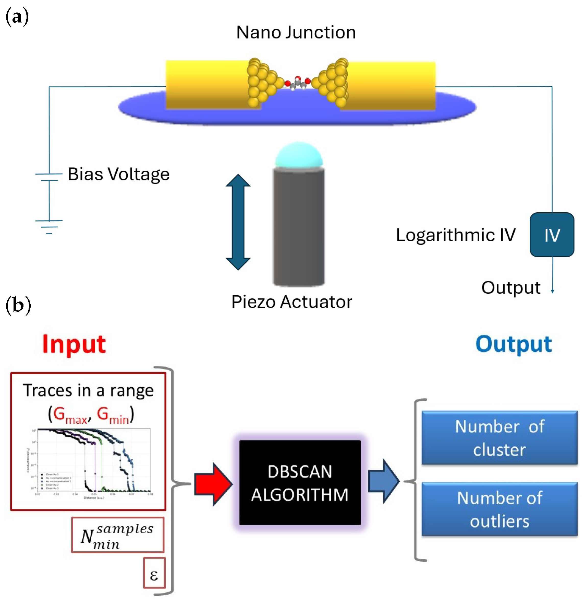
To investigate atomic-scale electronic transport under ambient conditions, we employed a mechanically controllable break junction (MCBJ) setup (see Figure 1a). This illustration shows a single molecule captured between two gold electrodes. A bias voltage is applied on the left side, and the current flows through a molecule trapped between the electrodes. These electrodes are mounted on a flexible polylactic acid (PLA) substrate. This substrate is bent using a piezoelectric actuator which, when pushed, causes the gold wire to break, and upon retraction, allows the flexible substrate to relax, bringing the electrodes back into contact and forming the junction again.
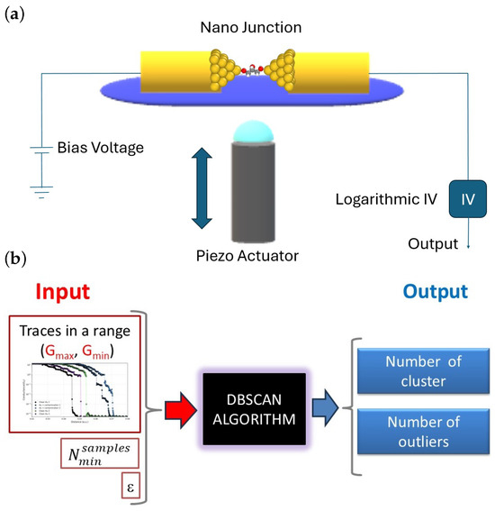
Figure 1.
(a) Illustration and basic circuit of a MCBJ. (b) Input and output sketch of the DBSCAN algorithm.
The current flowing through the molecule is extremely small, typically in the nanoampere or sub-nanoampere range. To accurately detect these low currents, a custom-built logarithmic I/V converter was used [29], allowing the amplification and recording of conductance signals as low as .
The system consists of a notched gold wire (Goodfellow, 0.1 mm diameter) carefully deposited and glued onto the flexible PLA substrate [30]. This configuration is integrated into a three-point bending mechanism, where a piezoelectric element provides precise mechanical control of the electrode separation, enabling the reproducible formation and rupture of atomic-scale junctions.
During the experiments, a constant bias voltage of 100 mV was applied across the junction. The resulting current was measured using the custom logarithmic I/V converter and recorded with a data acquisition (DAQ) system. This setup enables the acquisition of conductance traces, defined as the conductance versus relative electrode displacement—measured in volts or, when calibrated, in angstroms.
In this study, we focus exclusively on rupture traces. A total of approximately 5024 traces were acquired and analyzed under ambient conditions (25 °C and 80% humidity).
2.2. Classification Method: Use of the DBSCAN Algorithm
Although there are various approaches to applying clustering techniques to the classification of conductance traces, in this manuscript, we have chosen to use the DBSCAN algorithm. While the k-means algorithm may be faster and more computationally efficient, we have preferred to sacrifice speed in favor of greater classification fidelity. DBSCAN is particularly effective when clusters exhibit relatively uniform density and there is a clear distinction between dense and sparse regions. Its operation is based on the following two key parameters: the neighborhood radius , which defines the maximum distance between two points to be considered neighbors, and the minimum number of samples required for a point to be considered a core point.
In our case, the goal of clustering is not to classify individual points, but rather to identify and classify segments or ranges within each conductance trace. To this end, each segment is transformed into a feature vector by interpolation, so the algorithm operates on these vectors rather than on the entire trace. This is illustrated in Figure 1b, where the inputs to the algorithm are the conductance ranges to be analyzed in each individual trace. It is important to note that, under this formulation, the parameters and are applied directly to the feature vector space, not to the individual points contained in the original traces.
As shown in Figure 1b, the left side indicates the following inputs: the segmentation range, the number of variables considered, and the value of . Once a set of trace segments is processed (in our case, 5024 segments), and specific values of and are set, the algorithm returns the number of identified clusters, as well as the number of traces that are not assigned to any cluster (classified as outliers). One of the main advantages of DBSCAN is precisely its ability to automatically identify these outliers.
Although DBSCAN does not require prior knowledge of the number of clusters, having this information can be advantageous. In our case, we already know that the data ideally separate into the following two clusters: one corresponding to clean traces and the other to contaminated ones. For a given segmentation range and specific parameters, we assess whether DBSCAN identifies these two groups. Any data that do not fit well into either cluster are classified as outliers. However, the optimal values of and are not known in advance.
Our goal is to distinguish between two types of conductance traces, or two clusters, as follows: one corresponding to clean traces and the other to contaminated ones. As shown in Figure 1b, the left panel illustrates the following inputs: the segmentation range, the number of variables considered, and the value of . Once a set of trace segments (in our case, 5024) is processed and specific values of and are set, DBSCAN returns the number of identified clusters and the outliers. In this work, we propose a systematic methodology to determine the optimal values of and . To do so, we construct a meshgrid over the parameter space and run DBSCAN for all combinations of values. For each parameter pair, we record the number of clusters and outliers. To automate the process, we developed a script in Python 3.12 that explores the parameter space and generates a 3D map, where the z-axis indicates the number of clusters and the color scale encodes the number of outliers. This visual tool provides an intuitive way to select an optimal parameter set for reliable classification. Once this plot is obtained, we refer to it as the result of a completed iteration.
However, in our protocol, we must perform two iterations of DBSCAN in two distinct ranges to successfully classify the traces. This strategy has allowed us to develop a robust protocol that accurately distinguishes between ultraclean traces and those contaminated by the environment, even enabling the estimation of the relative percentage of each type. It is worth noting that the complete application of the protocol takes no more than ten minutes per dataset.
3. Results
3.1. Data Raw Atomic-Sized Contacts of Gold at Room Conditions
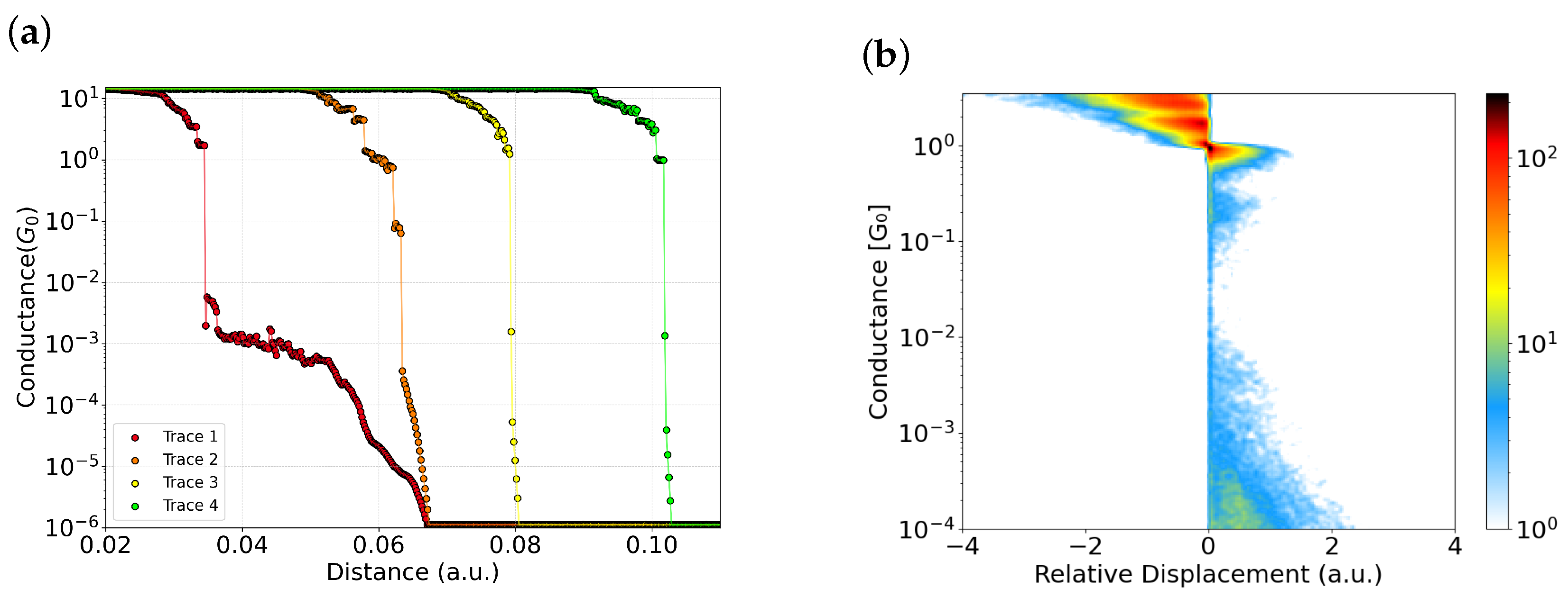
Figure 2a shows a selection of traces from the same experiment, plotted on a logarithmic scale relative to displacement. It is well known that when an atomic contact is clean, the conductance drops sharply to the tunneling regime after the final atomic plateau at upon further elongation [31,32,33]. In contrast, when a molecule is present between the electrodes, a plateau often appears in the sub-quantum conductance range due to its low transmission [16]. Traces 1 and 2 in Figure 2a exhibit conductance plateaus between and , despite the absence of any intentionally deposited molecules. This behavior suggests the presence of contamination, potentially due to unintentional molecular junctions or residual species influencing the conductance. In contrast, traces 3 and 4 drop abruptly from to below , without exhibiting any intermediate plateaus; these can therefore be classified as clean traces.
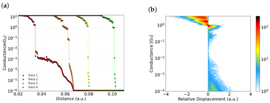
Figure 2.
(a) Representative conductance rupture traces plotted on a logarithmic scale. Traces 1 and 2 exhibit intermediate plateaus between and , suggesting the presence of molecular species or contaminants. In contrast, traces 3 and 4 show direct transitions from to below without intermediate features—clean traces. (b) Density map of 5024 gold rupture traces recorded at room temperature. The color scale reflects the number of events, with warm colors indicating high density and cool colors low density.
An alternative statistical representation is the density color map, which can be constructed by aligning all traces with respect to the onset of the last plateau corresponding to the single-atom contact (in the case of gold ). Specifically, each trace is shifted such that the first point at is set to zero displacement. This procedure is applied to all traces, allowing them to share a common reference point.
Using this alignment method, a density map is generated, as shown in Figure 2b, representing the full dataset composed of 5024 conductance traces. The map displays the number of events using a color scale as follows: warm colors (dark red) indicate high occurrence density, while cool colors (blue) denote low density. The plot is constructed with 245 bins along the x-axis and 250 bins along the y-axis and is subsequently smoothed.
3.2. Automated Selection of Optimal DBSCAN Parameters for Trace Classification
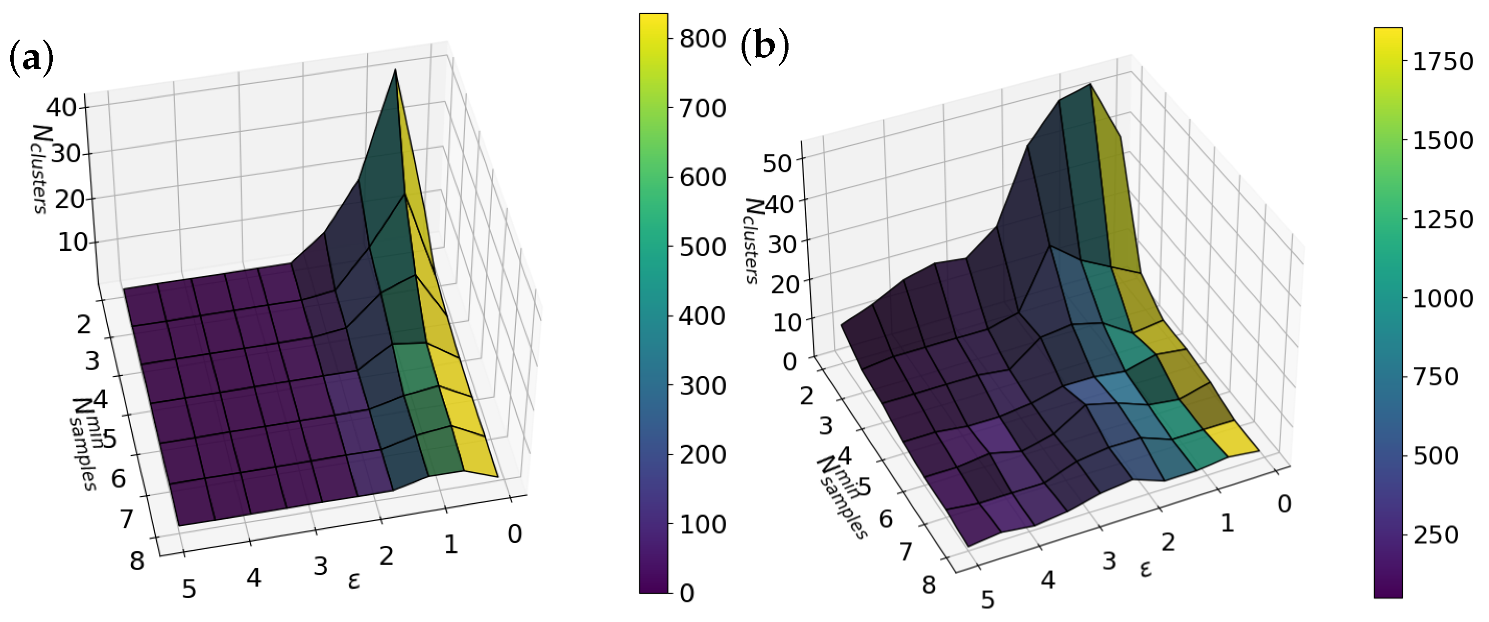
As explained earlier, DBSCAN depends on the following two parameters: and . To choose them automatically, we created a Python script that scans the parameter space. For each pair of values, it runs DBSCAN and records the number of clusters and outliers. The results are shown in a 3D plot where the x- and y-axes represent the parameters, the z-axis shows the number of clusters, and the color scale indicates the number of outliers. This makes it easy to spot the most suitable region, as shown by both panels in Figure 3.
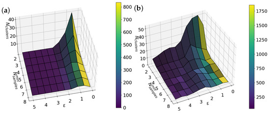
Figure 3.
Three-dimensional plots showing the number of clusters (z-axis) as a function of the DBSCAN parameters and . The color scale indicates the number of outliers detected. (a) Corresponds to the first iteration and (b) to the second iteration of DBSCAN.
However, as previously noted in the Materials and Methods section, a single DBSCAN iteration is not sufficient to accurately discriminate between fully clean and contaminated traces. For this reason, our protocol involves two successive DBSCAN runs, each applied to a different segment of the conductance traces. In the first iteration, the conductance traces are segmented in the range . This segment is used as input for a parameter sweep over and using a meshgrid approach. For each parameter pair, we compute the number of clusters and outliers identified by DBSCAN. The results are visualized in Figure 3a.
From the 3D map, we identify an optimal region where the number of clusters is two and is between 4 and 7. Selecting parameters in this region helps the algorithm detect well-defined clusters associated with clean traces. Table 1 shows a brief summary of the four selected possible DBSCAN parameter combinations explored. The first column shows the number of the combination. The second and third columns show the values of and , which yield exactly two clusters—matching the classification objective. The last three columns indicate the number of outliers, clean traces, and contaminated traces.

Table 1.
Summary of the possible DBSCAN parameter combinations explored in the first iteration.
As shown in Table 1, for values between approximately 1.5 and 4.5 and between 6 and 7, the number of traces classified as clean remains constant at 4188. Within this range, the number of outliers varies between 1 and 76, while the number of contaminated traces ranges from 760 to 836, always exceeding a total of 5024 traces. In this first iteration, we selected combinations 3 and 4, as both yield the minimum number of outliers (1) and allow the remaining traces to be classified as contaminated without affecting the number of clean traces. Since both combinations produce equivalent results, we adopted option 3 (or 4) as the reference for the next iteration. However, as clearly shown in Figure 4a, a noticeable cloud of counts remains in the region around , indicating that the separation is not entirely clean. In fact, the data raw density plot in Figure 2b, which includes all unfiltered traces (including contaminated ones), appears strikingly similar to the distribution obtained after the first DBSCAN filtering shown in Figure 4a. Therefore, a second iteration is warranted, as previously outlined in the Materials and Methods section of this manuscript.
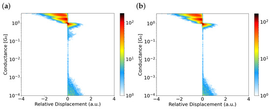
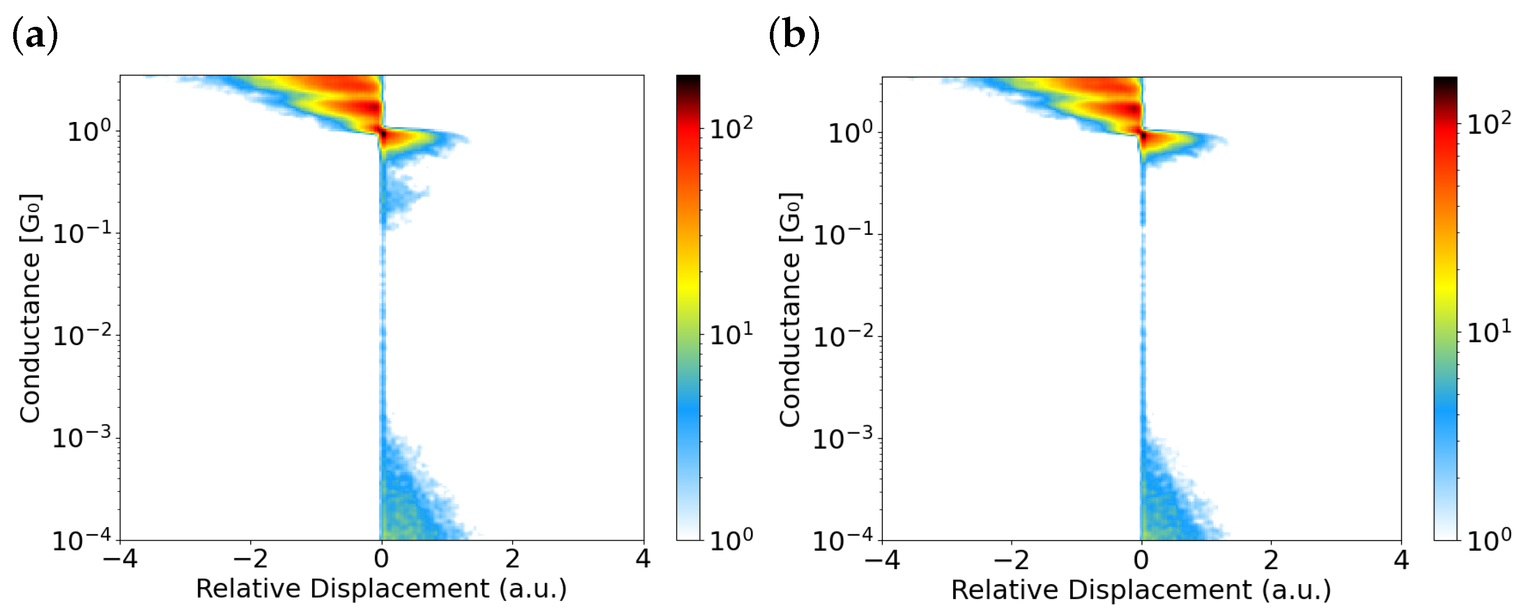
Figure 4.
Panel (a) shows a density plot constructed from the 4188 clean traces identified in the first iteration using combination 3–4 from Table 1. Panel (b) displays a density plot based on the 3912 clean traces identified in the second iteration using combination 2 from Table 2. The number of bins used for the density plots are 250 and 300, respectively.
In the second iteration, the same procedure is applied to a different segment of the conductance traces, , over the 4188 clean traces. The results obtained are shown in Figure 3b. This second analysis serves to refine the classification and helps distinguish really clean traces or traces with contaminants, completing the overall protocol.
As in the first iteration, we compile a summary table to evaluate different DBSCAN parameter combinations that result in two clusters. Table 2 presents these combinations. Based on this table, we observe that for very small values of , the number of outliers increases significantly. Upon inspection, this behavior appears to misclassify some genuinely clean traces as outliers. On the other hand, when is too large, the number of outliers drops drastically. However, the visual inspection of the supposedly clean traces reveals the presence of residual sub-plateaus in certain regions, suggesting that some contaminated traces are being misclassified as clean. Therefore, we select an intermediate value of , which results in a reasonable number of outliers and a sufficiently high number of clean traces. Specifically, out of the initial 4188 clean traces, 3912 are retained after this second filtering step.
Table 2.
Summary of the possible DBSCAN parameter combinations explored in the second iteration.
3.3. Clustering Based on DBSCAN to Identify Pure Metallic Atomic-Scale Gold Contacts and Traces with Contamination
Once the DBSCAN algorithm has been applied to classify the traces as clean or contaminated, one of the most effective ways to evaluate its performance is to represent both iterations using density plots. Figure 4 displays the following results: panel (a) shows the density plot from the first iteration, while panel (b) corresponds to the second iteration, in which traces identified as completely clean are shown.
As can be observed, the contaminated traces shown in Figure 4a behave quite differently. Around , a bluish cloud is clearly visible, indicating contamination. In contrast, the density plot in panel (b) exhibits very few counts within a noticeable gap between the atomic contact of gold (∼) and the tunneling regime (which starts around and is characterized by its slope on the logarithmic scale). Although a small number of points remain in this clear gap, the number of counts in this gap is three orders of magnitude compared to the maximum. These isolated points are typically attributed to artifacts from the data acquisition system (DAQ).
These qualitative differences between the two density plots confirm that they reflect distinct physical behaviors. A more detailed discussion supporting the validity of our classification algorithm is provided in the following section.
4. Discussion
Thanks to the DBSCAN clustering algorithm applied following the protocol described above, we have been able to classify conductance traces into two well-defined groups as follows: those confidently labeled as clean—even under ambient conditions—and those interpreted as affected by contamination. This classification is clearly reflected in the density plots shown in Figure 4. Panel (a) corresponds to the first iteration, which fails to correctly identify clean traces, while panel (b) shows the result of the second iteration, where clean traces are clearly isolated.
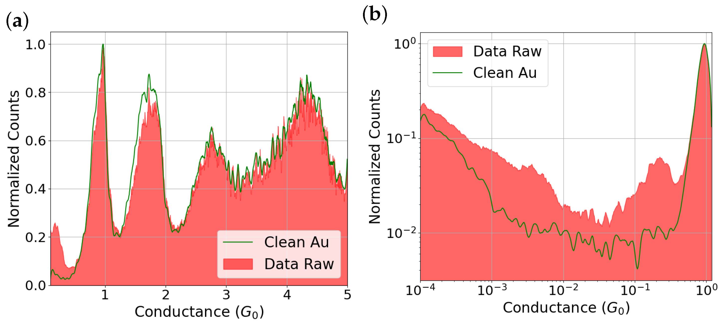
Moreover, we want to bring clarity to our message and to more conclusively demonstrate the cleanliness of the selected traces. Therefore, we propose an additional statistical analysis based on normalized conductance histograms (to one quantum of conductance), presented in both linear and logarithmic scales (see Figure 5). In these histograms, we compare the raw dataset with the subset of 3912 traces identified as clean. The color code indicates red for the raw data and green for the data classified as clean.
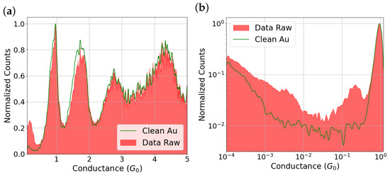
Figure 5.
Panel (a) shows the histogram on a linear scale, while panel (b) presents it on a logarithmic scale (log–log). The red curves correspond to the raw dataset (5024 traces), and the green curves represent the subset of 3912 clean traces identified by the DBSCAN algorithm.
The linear-scale histogram allows us to observe high conductance features and directly compare the overall profile of the raw (red) and clean datasets (green). In contrast, the log–log histogram (logarithmic in both counts and conductance) enhances the visibility of features typically associated with environmental contamination, such as peaks around or even down to . As expected, the log–log representation emphasizes all differences, especially in the low-conductance region. Finally, we provide a comparative table showing the number of traces classified as clean and contaminated within our dataset.
To further assess the robustness of our clustering procedure, we analyze the conductance histograms in the range from 0.1 to 5 for both the raw data (red color) and the clean subset (green line). As shown in Figure 5a, the histogram of the full dataset exhibits a strong peak centered around 1 , consistent with the typical conductance of single-atom Au contacts. Focusing on the peaks at 1, 2, and 3 , we observe that, for both the raw data and the clean dataset, the peak positions remain essentially the same, with only subtle differences. A slight decrease in the count density is noticeable near 2 for the clean traces. Interestingly, and in contrast with previous studies where molecules are deposited on gold atomic contacts—where a significant broadening of the 1 peak is typically observed [34,35]—such broadening is absent in our data, suggesting that environmental contamination does not produce a comparable effect.
However, a notable difference emerges in the low-conductance regime, around 0.1 . In this region, a clear peak appears in the raw dataset but is entirely absent in the clean traces. This highlights the importance of representing conductance histograms in a logarithmic scale, which allows for better resolution in the low-conductance region and helps reveal the true positions and nature of such peaks, potentially masked in linear representations.
The distinction between clean and contaminated traces is clearly observed in the log–log scale histograms in Figure 5b. In the clean dataset (represented by the green histogram), there is a marked dip in the count density, specifically between approximately and . Below this threshold, the histogram exhibits a linear trend on the log–log scale, which is a characteristic behavior of the tunneling regime. Conversely, the raw data (red area) displays a prominent distribution of conductance values within the same range. Here, a significant concentration of events stands out, centered around . This peak is commonly associated with contamination from environmental sources or hydrocarbons, as confirmed in our previous study [34]. It is crucial to note that the count density of this peak in the contaminated histogram, close to , is almost an order of magnitude higher compared to the clean traces. The latter, in contrast, show no distinct peak in this region, only baseline counts. Furthermore, another prominent feature exists in the contaminated data, disrupting the linear trends observed in the clean traces within the to range. This deviation is also attributed to contamination, given that no molecules were intentionally deposited and, under ideal conditions, no counts should appear in this range.
With all these data, we can quantitatively determine the percentage of clean and contaminated traces obtained after applying our classification process. This statistical analysis allows us to evaluate whether our samples progressively degrade over time due to environmental exposure, or if contamination occurs immediately upon exposure.
The following Table 3 summarizes the total number of traces analyzed, along with the relative proportions of clean and contaminated traces.
Table 3.
Statistical summary of trace classification.
Altogether, the combined visual and statistical analyses support the effectiveness of our DBSCAN-based classification. The subset of clean traces not only excludes contamination artifacts but also reproduces features known from high-purity, low-temperature measurements. This reinforces the reliability of our approach and demonstrates that meaningful structural and electronic information can be extracted from ambient-condition experiments, provided that appropriate data-cleaning procedures are applied.
5. Conclusions
Therefore, we conclude that we have developed a robust trace classification procedure capable of separating clean and contaminated traces through a two-step DBSCAN-based protocol. This methodology enables a quantitative evaluation of the proportion of clean versus contaminated traces within a dataset. In our case, we determined that of the traces are completely clean, meaning they do not exhibit any counts or plateaus in the range of [] .
Importantly, this constitutes the first compact device that, via electronic transport measurements, can quantify the presence of a single contaminant molecule. Although it does not provide information about the chemical identity of the contaminant, it reliably assesses its abundance.
These findings demonstrate that a large fraction of the traces are of high purity. Furthermore, our methodology could be extended to evaluate how different metals degrade upon exposure to environmental conditions. This, in turn, would support decisions about whether molecular deposition is justified or help define the minimum contamination threshold required for reproducible and reliable molecular-scale measurements.
Author Contributions
G.P. contributed to the methodology, software development, investigation, and data analysis. C.S. contributed to the conceptualization; methodology; validation; formal analysis; investigation; resources; supervision; writing—original draft, review, and editing; and funding acquisition. All authors have read and agreed to the published version of the manuscript.
Funding
This work received financial support from the Generalitat Valenciana through CIDEXG/2022/45. This research is an integral part of the Advanced Materials program, supported by MCIN with funding from the European Union NextGenerationEU (PRTR-C17.I1) and the Generalitat Valenciana (MFA/2022/045). We also acknowledge funding from MICIU/AEI/10.13039/501100011033 and the European Regional Development Fund (ERDF/EU) under project PID2023-146660OB-I00.
Data Availability Statement
The original contributions presented in this study are included in the article. Further inquiries can be directed to the corresponding author.
Acknowledgments
The authors extend their gratitude for the insightful discussions to Carlos Untiedt, Wynand Dednam, Tamara de Ara, Andrés Martínez, Juan Pablo Cuenca, and Enrique Guzmán.
Conflicts of Interest
The authors declare no conflicts of interest.
Abbreviations
The following abbreviations are used in this manuscript:
| MCBJ | Mechanical Controllable Break Junctions |
| DBSCAN | Density-Based Spatial Clustering of Applications with Noise |
References
- Agraït, N.; Yeyati, A.L.; Van Ruitenbeek, J.M. Quantum properties of atomic-sized conductors. Phys. Rep. 2003, 377, 81–279. [Google Scholar] [CrossRef]
- Cuevas, J.C.; Scheer, E. Molecular Electronics, 2nd ed.; World Scientific: Singapore, 2017. [Google Scholar] [CrossRef]
- Evers, F.; Korytár, R.; Tewari, S.; van Ruitenbeek, J.M. Advances and challenges in single-molecule electron transport. Rev. Mod. Phys. 2020, 92, 035001–035065. [Google Scholar] [CrossRef]
- Pascual, J.I.; Méndez, J.; Gómez-Herrero, J.; Baró, A.M.; García, N.; Binh, V.T. Quantum contact in gold nanostructures by scanning tunneling microscopy. Phys. Rev. Lett. 1993, 71, 1852–1855. [Google Scholar] [CrossRef] [PubMed]
- Krans, J.M.; Muller, C.J.; Yanson, I.K.; Govaert, T.C.M.; Hesper, R.; van Ruitenbeek, J.M. One-atom point contacts. Phys. Rev. B 1993, 48, 14721–14724. [Google Scholar] [CrossRef] [PubMed]
- Krans, J.M.; van Ruitenbeek, J.M. Subquantum conductance steps in atom-sized contacts of the semimetal Sb. Phys. Rev. B 1994, 50, 17659–17661. [Google Scholar] [CrossRef]
- Krans, J.M.; van Ruitenbeek, J.M.; Fisun, V.V.; Yanson, I.K.; de Jongh, L.J. The signature of conductance quantization in metallic point contacts. Nature 1995, 375, 767–769. [Google Scholar] [CrossRef]
- Landauer, R. Spatial Variation of Currents and Fields Due to Localized Scatterers in Metallic Conduction. IBM J. Res. Dev. 1957, 1, 223–231. [Google Scholar] [CrossRef]
- van Wees, B.J.; van Houten, H.; Beenakker, C.W.J.; Williamson, J.G.; Kouwenhoven, L.P.; van der Marel, D.; Foxon, C.T. Quantized conductance of point contacts in a two-dimensional electron gas. Phys. Rev. Lett. 1988, 60, 848–850. [Google Scholar] [CrossRef]
- Agraït, N.; Rodrigo, J.G.; Vieira, S. Conductance steps and quantization in atomic-size contacts. Phys. Rev. B 1993, 47, 12345–12348. [Google Scholar] [CrossRef]
- Pan, X.; Qian, C.; Chow, A.; Wang, L.; Kamenetska, M. Atomically precise binding conformations of adenine and its variants on gold using single molecule conductance signatures. J. Chem. Phys. 2022, 157, 234201. [Google Scholar] [CrossRef]
- Smit, R.H.M.; Noat, Y.; Untiedt, C.; Lang, N.D.; van Hemert, M.C.; van Ruitenbeek, J.M. Measurement of the conductance of a hydrogen molecule. Nature 2002, 419, 906–909. [Google Scholar] [CrossRef] [PubMed]
- Kim, Y.; Pietsch, T.; Erbe, A.; Belzig, W.; Scheer, E. Benzenedithiol: A Broad-Range Single-Channel Molecular Conductor. Nano Lett. 2011, 11, 3734–3738. [Google Scholar] [CrossRef] [PubMed]
- Tewari, S.; Sabater, C.; van Ruitenbeek, J. Identification of vibration modes in single-molecule junctions by strong inelastic signals in noise. Nanoscale 2019, 11, 19462–19467. [Google Scholar] [CrossRef]
- Reed, M.; Zhou, C.; Muller, C.; Burgin, T.; Tour, J. Conductance of a molecular junction. Science 1997, 278, 252–254. [Google Scholar] [CrossRef]
- Xu, B.; Tao, N.J. Measurement of Single-Molecule Resistance by Repeated Formation of Molecular Junctions. Science 2003, 301, 1221–1223. [Google Scholar] [CrossRef] [PubMed]
- Herrer, I.L.; Ismael, A.K.; Milán, D.C.; Vezzoli, A.; Martín, S.; González-Orive, A.; Grace, I.; Lambert, C.; Serrano, J.L.; Nichols, R.J.; et al. Unconventional Single-Molecule Conductance Behavior for a New Heterocyclic Anchoring Group: Pyrazolyl. J. Phys. Chem. Lett. 2018, 9, 5364–5372. [Google Scholar] [CrossRef] [PubMed]
- Montenegro-Pohlhammer, N.; Sánchez-de Armas, R.; Calzado, C.J.; Borges-Martínez, M.; Cárdenas-Jirón, G. A photo-induced spin crossover based molecular switch and spin filter operating at room temperature. Dalton Trans. 2021, 50, 6578–6587. [Google Scholar] [CrossRef]
- de Ara, T.; Hsu, C.; Martinez-Garcia, A.; Baciu, B.C.; Bronk, P.J.; Ornago, L.; van der Poel, S.; Lombardi, E.B.; Guijarro, A.; Sabater, C.; et al. Evidence of an Off-Resonant Electronic Transport Mechanism in Helicenes. J. Phys. Chem. Lett. 2024, 15, 8343–8350. [Google Scholar] [CrossRef] [PubMed]
- Singh, A.K.; Martin, K.; Mastropasqua Talamo, M.; Houssin, A.; Vanthuyne, N.; Avarvari, N.; Tal, O. Single-molecule junctions map the interplay between electrons and chirality. Nat. Commun. 2025, 16, 1759. [Google Scholar] [CrossRef]
- Cabosart, D.; El Abbassi, M.; Stefani, D.; Frisenda, R.; Calame, M.; van der Zant, H.S.J.; Perrin, M.L. A reference-free clustering method for the analysis of molecular break-junction measurements. Appl. Phys. Lett. 2019, 114, 143102. [Google Scholar] [CrossRef]
- Liu, B.; Murayama, S.; Komoto, Y.; Tsutsui, M.; Taniguchi, M. Dissecting Time-Evolved Conductance Behavior of Single Molecule Junctions by Nonparametric Machine Learning. J. Phys. Chem. Lett. 2020, 11, 6567–6572. [Google Scholar] [CrossRef] [PubMed]
- Lin, L.; Tang, C.; Dong, G.; Chen, Z.; Pan, Z.; Liu, J.; Yang, Y.; Shi, J.; Ji, R.; Hong, W. Spectral Clustering to Analyze the Hidden Events in Single-Molecule Break Junctions. J. Phys. Chem. C 2021, 125, 3623–3630. [Google Scholar] [CrossRef]
- Bro-Jørgensen, W.; Hamill, J.M.; Bro, R.; Solomon, G.C. Trusting our machines: Validating machine learning models for single-molecule transport experiments. Chem. Soc. Rev. 2022, 51, 6875–6892. [Google Scholar] [CrossRef]
- Komoto, Y.; Ryu, J.; Taniguchi, M. Machine learning and analytical methods for single-molecule conductance measurements. Chem. Commun. 2023, 59, 6796–6810. [Google Scholar] [CrossRef] [PubMed]
- Ester, M.; Kriegel, H.P.; Sander, J.; Xu, X. A density-based algorithm for discovering clusters in large spatial databases with noise. In Proceedings of the Second International Conference on Knowledge Discovery and Data Mining, KDD’96, Portland, OR, USA, 2–4 August 1996; pp. 226–231. [Google Scholar]
- Ester, M. Chapter 5—Density-Based Clustering. In Data Clustering, 1st ed.; Chapman and Hall/CRC: Boca Raton, FL, USA, 2014; p. 17. [Google Scholar]
- Schubert, E.; Sander, J.; Ester, M.; Kriegel, H.P.; Xu, X. DBSCAN Revisited, Revisited: Why and How You Should (Still) Use DBSCAN. ACM Trans. Database Syst. (TODS) 2017, 42, 1–21. [Google Scholar] [CrossRef]
- Ornago, L. Complexity of Electron Transport in Nanoscale Molecular Junctions. Ph.D. Dissertation, Delft University of Technology, Delft, The Netherlands, 2023. [Google Scholar]
- Cuenca, J.P.; de Ara, T.; Martinez-Garcia, A.; Guzman, F.; Sabater, C. Exploring Three-Atom-Thick Gold Structures as a Benchmark for Atomic-Scale Calibration of Break-Junction Systems. arXiV 2025. [Google Scholar] [CrossRef]
- Gimzewski, J.K.; Möller, R. Transition from the tunneling regime to point contact studied using scanning tunneling microscopy. Phys. Rev. B 1987, 36, 1284–1287. [Google Scholar] [CrossRef]
- Untiedt, C.; Caturla, M.J.; Calvo, M.R.; Palacios, J.J.; Segers, R.C.; van Ruitenbeek, J.M. Formation of a Metallic Contact: Jump to Contact Revisited. Phys. Rev. Lett. 2007, 98, 206801. [Google Scholar] [CrossRef]
- Sabater, C.; Caturla, M.J.; Palacios, J.J.; Untiedt, C. Understanding the structure of the first atomic contact in gold. Nanoscale Res. Lett. 2013, 8, 257. [Google Scholar] [CrossRef] [PubMed]
- de Ara, T.; Sabater, C.; Borja-Espinosa, C.; Ferrer-Alcaraz, P.; Baciu, B.C.; Guijarro, A.; Untiedt, C. Signature of adsorbed solvents for molecular electronics revealed via scanning tunneling microscopy. Mater. Chem. Phys. 2022, 291, 126645. [Google Scholar] [CrossRef]
- Martinez-Garcia, A.; de Ara, T.; Pastor-Amat, L.; Untiedt, C.; Lombardi, E.B.; Dednam, W.; Sabater, C. Unraveling the Interplay between Quantum Transport and Geometrical Conformations in Monocyclic Hydrocarbons’ Molecular Junctions. J. Phys. Chem. C 2023, 127, 23303–23311. [Google Scholar] [CrossRef] [PubMed]
Disclaimer/Publisher’s Note: The statements, opinions and data contained in all publications are solely those of the individual author(s) and contributor(s) and not of MDPI and/or the editor(s). MDPI and/or the editor(s) disclaim responsibility for any injury to people or property resulting from any ideas, methods, instructions or products referred to in the content. |
© 2025 by the authors. Licensee MDPI, Basel, Switzerland. This article is an open access article distributed under the terms and conditions of the Creative Commons Attribution (CC BY) license (https://creativecommons.org/licenses/by/4.0/).