Article

Deposition of Boron-Doped Thin CVD Diamond Films from Methane-Triethyl Borate-Hydrogen Gas Mixture

by
Nikolay Ivanovich Polushin
1,
Alexander Ivanovich Laptev
1,
Boris Vladimirovich Spitsyn
2,
Alexander Evgenievich Alexenko
2,
Alexander Mihailovich Polyansky
3,
Anatoly Lvovich Maslov
1,* and
Tatiana Vladimirovna Martynova
1
1
Research Laboratory of Superhard Materials, National University of Science and Technology MISIS, Leninsky avenue, 4, Moscow 119049, Russia
2
Institute of Physical Chemistry, Russian Academy of Sciences, Leninsky avenue, 31, Moscow 119991, Russia
3
JSC “NPO Energomash named after Academician V.P. Glushko”, Burdenko street, 1, Khimki 141401, Russia
*
Author to whom correspondence should be addressed.
Processes 2020, 8(6), 666; https://doi.org/10.3390/pr8060666
Submission received: 30 April 2020 / Revised: 30 May 2020 / Accepted: 2 June 2020 / Published: 4 June 2020
(This article belongs to the Special Issue Synthesis and Application of Nano- and Microdispersed Systems)

Abstract

:
Boron-doped diamond is a promising semiconductor material that can be used as a sensor and in power electronics. Currently, researchers have obtained thin boron-doped diamond layers due to low film growth rates (2–10 μm/h), with polycrystalline diamond growth on the front and edge planes of thicker crystals, inhomogeneous properties in the growing crystal’s volume, and the presence of different structural defects. One way to reduce structural imperfection is the specification of optimal synthesis conditions, as well as surface etching, to remove diamond polycrystals. Etching can be carried out using various gas compositions, but this operation is conducted with the interruption of the diamond deposition process; therefore, inhomogeneity in the diamond structure appears. The solution to this problem is etching in the process of diamond deposition. To realize this in the present work, we used triethyl borate as a boron-containing substance in the process of boron-doped diamond chemical vapor deposition. Due to the oxygen atoms in the triethyl borate molecule, it became possible to carry out an experiment on simultaneous boron-doped diamond deposition and growing surface etching without the requirement of process interruption for other operations. As a result of the experiments, we obtain highly boron-doped monocrystalline diamond layers with a thickness of about 8 μm and a boron content of 2.9%. Defects in the form of diamond polycrystals were not detected on the surface and around the periphery of the plate.

1. Introduction

Today, there is a significant number of publications devoted to the study of electrophysical properties of boron-doped single-crystal synthetic diamond [1,2,3,4,5,6,7]. Other works are devoted to reviews of the mechanism and optimal conditions for thin diamond layer deposition; some of these works are connected with boron-doped diamonds [8,9,10,11]. In [12,13], it was shown that the thicker the diamond layer is grown, the higher the probability of defects occurring at its growing surface. The number of defects is notably affected by the single-crystal CVD-diamond (chemical vapor deposition-diamond) deposition rate: the probability of defect formation and their number per unit area grows with the increase of deposition rate. Therefore, boron-doped single-crystal diamond thin films are grown at a low deposition rate. The necessity of intermediate treatment of the obtained samples and loading of new substrates into the reactor chamber leads to the expenditure of large amounts of time and resources. Such production costs lead to higher costs and lower output of the product.
To reduce the cost of production (for example, sensors or crystals for power electronics) and to increase production, growing thick homogeneous boron-doped single-crystal CVD-diamond layers was proposed as rough material for the jewelry industry or for cutting thin doped diamond plates for subsequent treatment.
Reducing the number of defects on the surface (Figure 1) and increasing the boron-doped single-crystal CVD-diamond deposition rate can be achieved by etching the surface of the growing diamond during the deposition process.
Apparently, it is necessary to keep the composition of the gas phase constant in order to receive stable properties over the whole volume of the diamond. In addition, controlling the nitrogen content in the diamond is unavoidable, which can be achieved by using high-purity substances. Oxygen could be added into the gas mixture to etch the surface of a growing diamond. In this case, the problem of synthesis of thick boron-doped single-crystal diamond films is narrowed down to solving the following subtasks:
  • To find an appropriate boron-containing substance.
  • To optimize the process of synthesis of boron-doped diamond of small thickness.
  • To optimize the process of synthesis of thick layers of boron-doped diamond due to its constant etching.
After the realization of the third point, it becomes possible not only to reduce the cost of semiconductor products significantly but also to obtain fancy-colored diamonds for the jewelry industry.
Today, researchers use various boron-containing compounds for doping diamond during its deposition from the gas phase; the most typical additives are demonstrated in Table 1.
As can be seen from Table 1, in most experiments, diborane is used for doping diamond with boron. This compound, under standard conditions, is a colorless gas with a nauseating sweet odor. Diborane is qualified as an unstable flammable substance. Besides this, this gas is highly toxic and poses a hazard to humans [28,29,30,31,32]. This substance is used as an acceptor dopant for epitaxial silicon in the industrial production of semiconductor materials. It is also used for doping silicon plates by the deposition/dispersion technique and polysilicon interconnection of some capacitors. Diborane is widely used in the formation of borosilicate glasses [33,34] and often used as a source of hydrogen in many chemical reactions [35].
Diborane belongs to the class of boranes. These compounds have high chemical reactivity, major heat of combustion, and they are not thermodynamically stable compounds of boron and hydrogen. Many of the boranes, due to the nuances listed above, belong to substances with the highest category of flammability: they can self-ignite from high temperatures not only in air but also in contact with water or a number of halogenated hydrocarbons [36]. Table 2 represents the characteristics of some boranes: their stability and behavior in air and water [37].
As a result of the analysis of Table 2, it is possible to conclude that boranes, except older boranes (starting with B6H10), are unstable compounds. At the same time, despite the absence of such a serious drawback, such as autoignition in the presence of oxygen, these boranes are not widely used in both scientific and industrial applications.
Diborane, which is prevalent in the semiconductor industry, is never used with oxygen. Trimethyl borate is more volatile, flammable, and faster hydrolyzed than triethyl borate. Trimethyl borate boils at 68 °C, triethyl borate at 119 °C [38].
Taking into account the properties of boranes, as well as the need to use oxygen to achieve the objectives, we decided to use triethyl borate (C2H5O)3B.

2. Materials and Methods

2.1. Materials

In this research, we used an excess of boric acid (99.9% purity) in ethyl alcohol (95% aqueous solution) as initial stock for triethyl borate. During the synthesis, a constant temperature of the mixture was maintained at 25 ± 1 °C. To input triethyl borate to the Ardis 300, we used a hydrogen blow with least 99.9995% purity. The methane purity was not less than 99.995%.
A single-crystal diamond with misorientation angles and directions that corresponded to the requirements for growing single-crystal diamonds was used as a substrate for deposition.

2.2. Scanning Electron Microscopy and X-ray Microanalysis

The study of the surface layers of the coatings was carried out on a HITACHI SU5000 scanning electron microscope equipped with annexes for X-ray spectral microanalysis X-MaxN and electron backscatter diffraction (EBSD) Nordlys Nano from OXFORD INSTRUMENTS. Phase identification was accomplished using the NIST Structural Database (NSD).

2.3. The Hardness and Elastic Modulus of Coatings

The hardness and elastic modulus of boron-doped diamond films were determined using the Oliver–Farr method [39,40] on a Micro Indentation Tester CSM-Instruments (Switzerland), using a Vickers diamond pyramid. The maximum load was 50.00 mN.
According to the Oliver–Farr method, hardness is the ratio of the maximum indentation load and the projection area of the indenter contact to the material without elastic deflection at the edge of the print (i.e., without the elastic component).
The formula for hardness is the following [41] (Figure 2):
H = F S = F k h c 2
where F—max force,
S—contact area,
h c depth of contact of the indenter with the material, defined as
h c = h m a x ε P m a x S = h m a x ε ( h m a x h i )
ε   a n d   k constants depending on the indenter geometry,
h i distance corresponding to the intersection of the tangent to the unloading curve at the beginning part of the displacement axis,
h m a x maximum depth of indenter penetration in the material.
Contact stiffness (S) is determined by the slope of the initial part of the unloading curve (Pmax):
S = ( d P d h ) P = P m a x

2.4. Preparing the Single-Crystal Diamond Surface and the Thin-Layer Doping Process

Figure 3 shows a schematic diagram of the single-crystal diamond substrate preparation for doping with boron and the subsequent treatment of products.
The preparation stages for materials and equipment, including the preparation of diamond substrates by etching, laser cutting, and subsequent mechanical treatment, are the same with the single-crystal diamond substrate preparation for high-purity single-crystal diamond deposition by the CVD process.
The process of substrates etching can be carried out in various atmospheres. For example, diamond is etched at a low rate in hydrogen plasma [42]; in oxygen-argon mixture, it is much higher and reaches 200 nm/min [43]; in an oxygen-hydrogen mixture (with up to 2% oxygen), the etching rate is more than 200 nm/min [44].
The doped single-crystal films were grown from the gas phase, which comprised methane, hydrogen, and a boron-containing substance, on single-crystal diamond substrates. To achieve this, as previously shown, trimethyl or triethyl borate can be used. These substances are obtained by mixing boric acid and alcohol—either methyl or ethyl. In this work, we used ethanol to prepare triethyl borate (C2H5O)3B. Electrolytically generated hydrogen after dehydration and purification was divided into two streams. A smaller part (5–15 cm3/min) was passed through a bubbler system with ethanol and boric acid that formed volatile triethyl borate. The second part of the hydrogen from the generator was input into the reactor. In order to keep the composition of the gas mixture unchanged during the whole process of deposition, we used a saturated solution of boric acid. Boric acid in the bubbler system was always maintained in excess. The bubbler system was placed in a thermostat at a temperature of 25 °C. Silica gel desiccant was used to dry the input mixture. The desiccant was a steel cylinder with a diameter of 40 mm and a length of 300 mm and it was filled with silica gel. For ease of exploitation (drying silica gel after work), the cylinder was equipped with a quick-detachable connection with a soldered metal mesh to exclude silica gel contact with the system.
Hydrocarbon radicals with high reactivity were formed in the gas phase as a result of the activation of the mixture of hydrogen, methane, and triethyl borate. As a result of decomposing hydrocarbon radicals on the substrate, free carbon and atomic hydrogen were released, which ensures the high selectivity of the diamond growth process due to the release of nondiamond carbon that could crystallize on the substrate [45].
The deposition process was carried out at 9.806 kPa pressure in the system. The substrate temperature was 1100 °C. The methane flow to the reactor was 25 cm3/min; the flow of a mixture of triethyl borate and hydrogen (with possible vapors of ethanol) was 10 cm3/min.
The required parameters of pressure and gas flow were maintained automatically. The duration of the deposition process was 2 h at a growth rate of 4 μm/h.

3. Results and Discussions

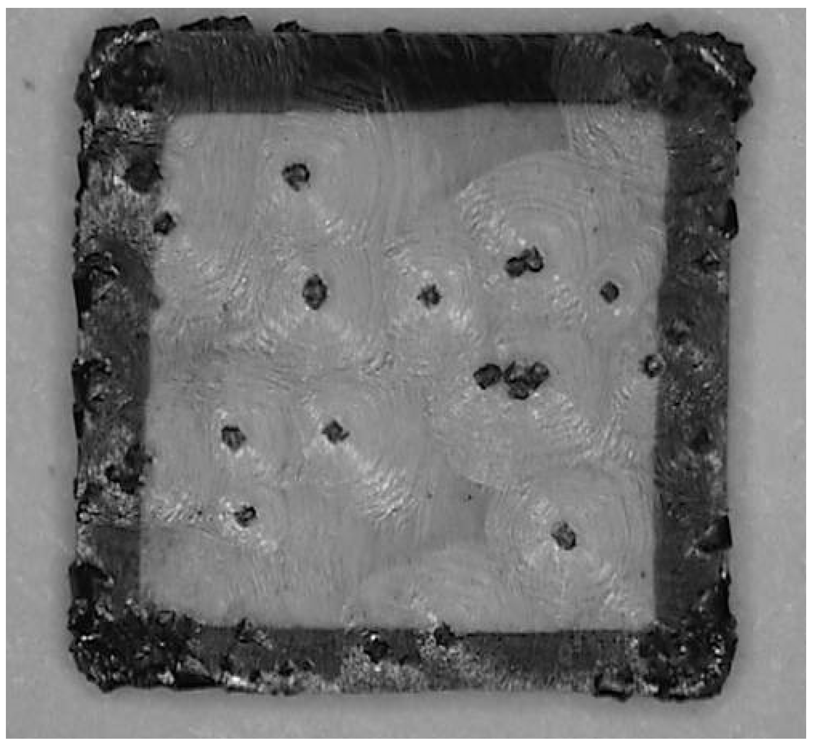
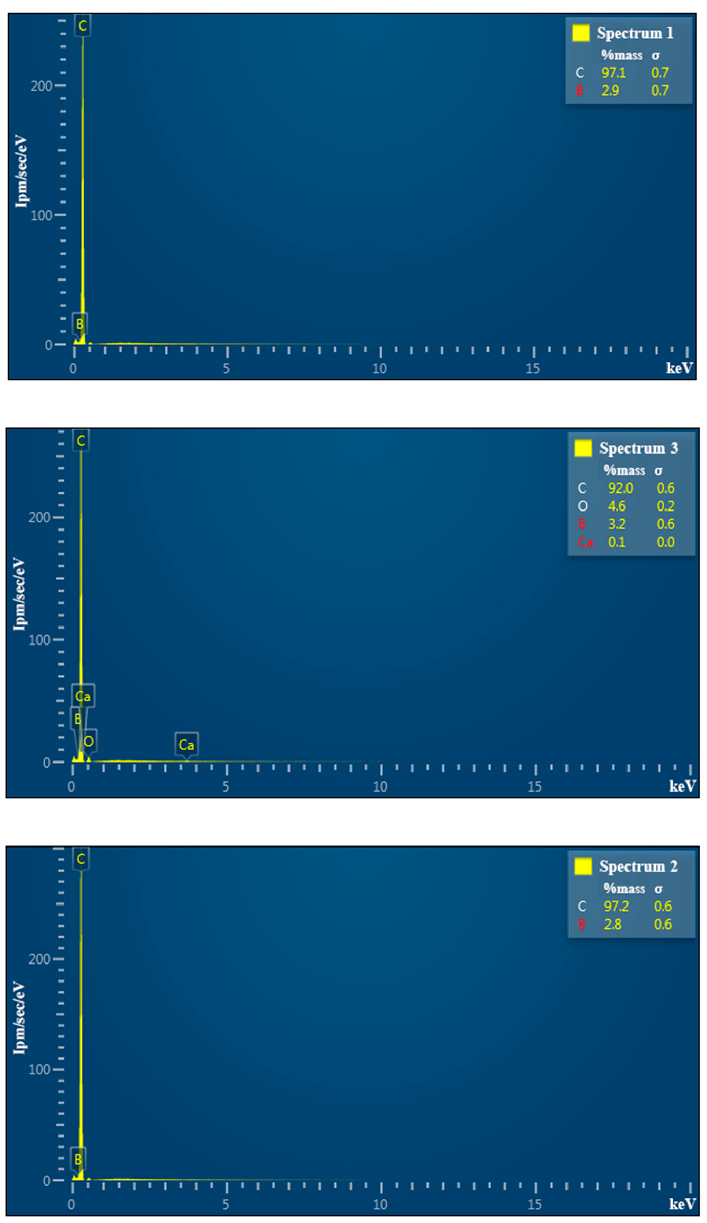
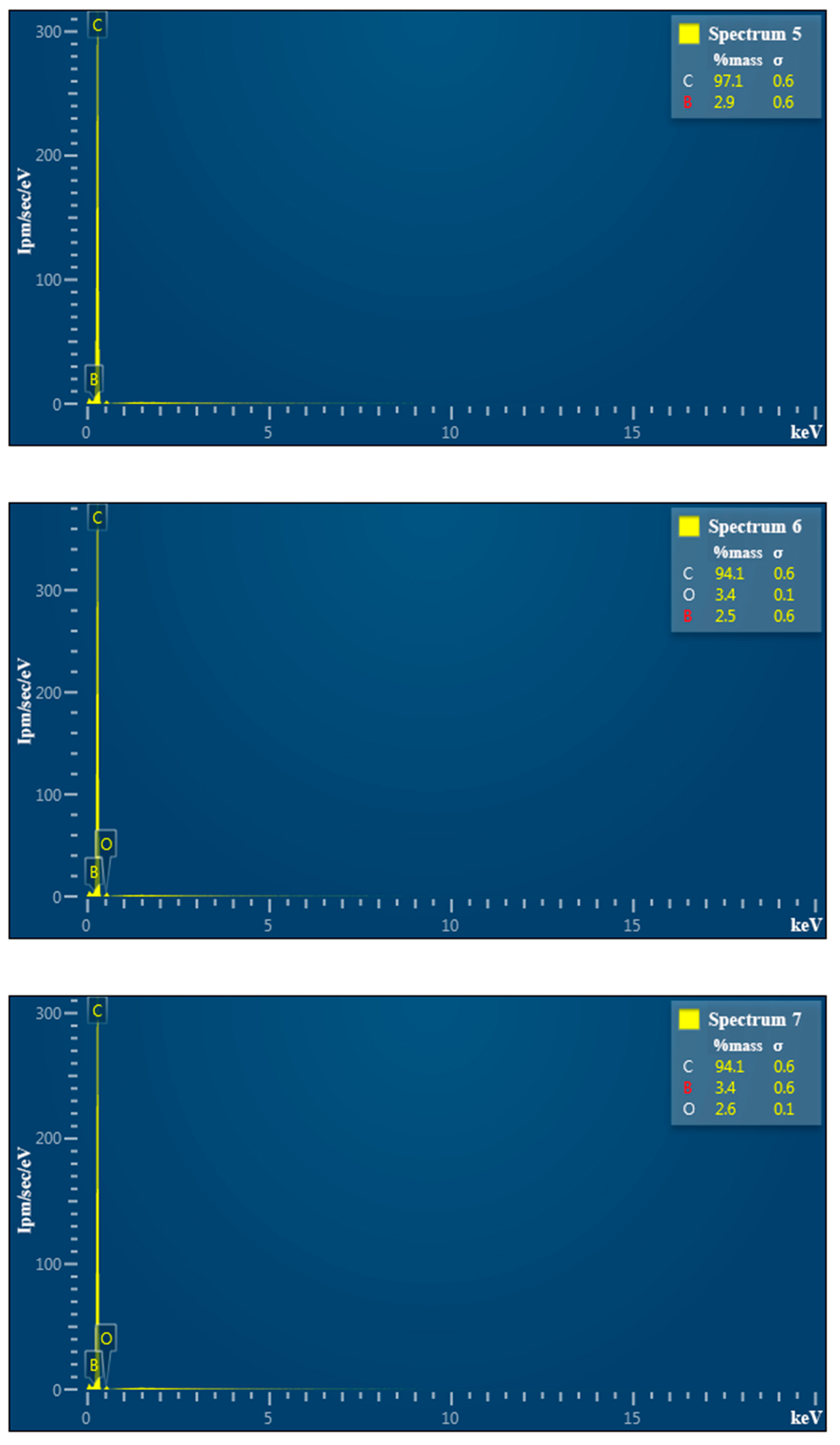
3.1. Scanning Electron Microscopy and Elemental Analysis

Figure 4 shows the samples obtained as a result of the experiments.
As seen in Figure 4, both samples have surfaces without such defects as on the example of the plate in Figure 1. A large amount of triethyl borate was supplied to the system with the purpose of increasing the oxygen concentration in the plasma. Obviously, such high concentrations of oxygen allowed etching defects. Figure 5 demonstrates the surface images of Samples 1 and 2 with boron-doped layers.
It can be seen that the surface of Sample 1 has growth “waves”. In addition, there are incoherent formations on it. The surface of Sample 2 also contains incoherent formations, but the growth “waves” are less noticeable.
The distribution of Sample 1 areas for determining the chemical composition using X-ray microanalysis is presented in Figure 6. Table 3 presents the results of Sample 1 surface X-ray microanalysis.
Table 3 (data from Figure 7), containing elemental analysis based on the EDS (energy-dispersive X-ray spectroscopy) results, demonstrates that the first position, as well as the second, corresponds to heavily boron-doped diamond with a boron content of 2.9%.
The third position is a foreign substance containing carbon, oxygen, and boron that corresponds to the composition of triethyl borate, which, apparently, could depose from the gas phase at the end of the diamond-doping process.
The distribution of Sample 2 areas for determining the chemical composition using X-ray microanalysis is presented in Figure 8. On the surface of Sample 2, as well as on Sample 1, there are a significant number of foreign formations.
Table 4 (data from Figure 9) contains elemental analysis based on the EDS and presents the results of Sample 2 surface X-ray microanalysis. The boron content in Sample 2 was 2.9%, as in Sample 1. Considering that samples were obtained in independent experiments with the same synthesis parameters, the result indicates high doping-process stability.
Positions 7 and 8 are a foreign substance corresponding to the composition of triethyl borate, which, apparently, could depose from the gas phase at the end of the diamond-doping process. To eliminate such defects in both cases, it will be sufficient to etch the obtained diamond surface in the stream of atomic hydrogen without doping or carbon-containing substances.
Using the EBSD method, we obtained electron diffraction patterns, indexed them, determined their phase composition, type of lattice, and orientation (Euler angles) in each of the six investigated areas. We revealed that the coating orientations in different areas were the same, which allowed us to conclude that the coating was single-crystal and was formed by epitaxial growth.

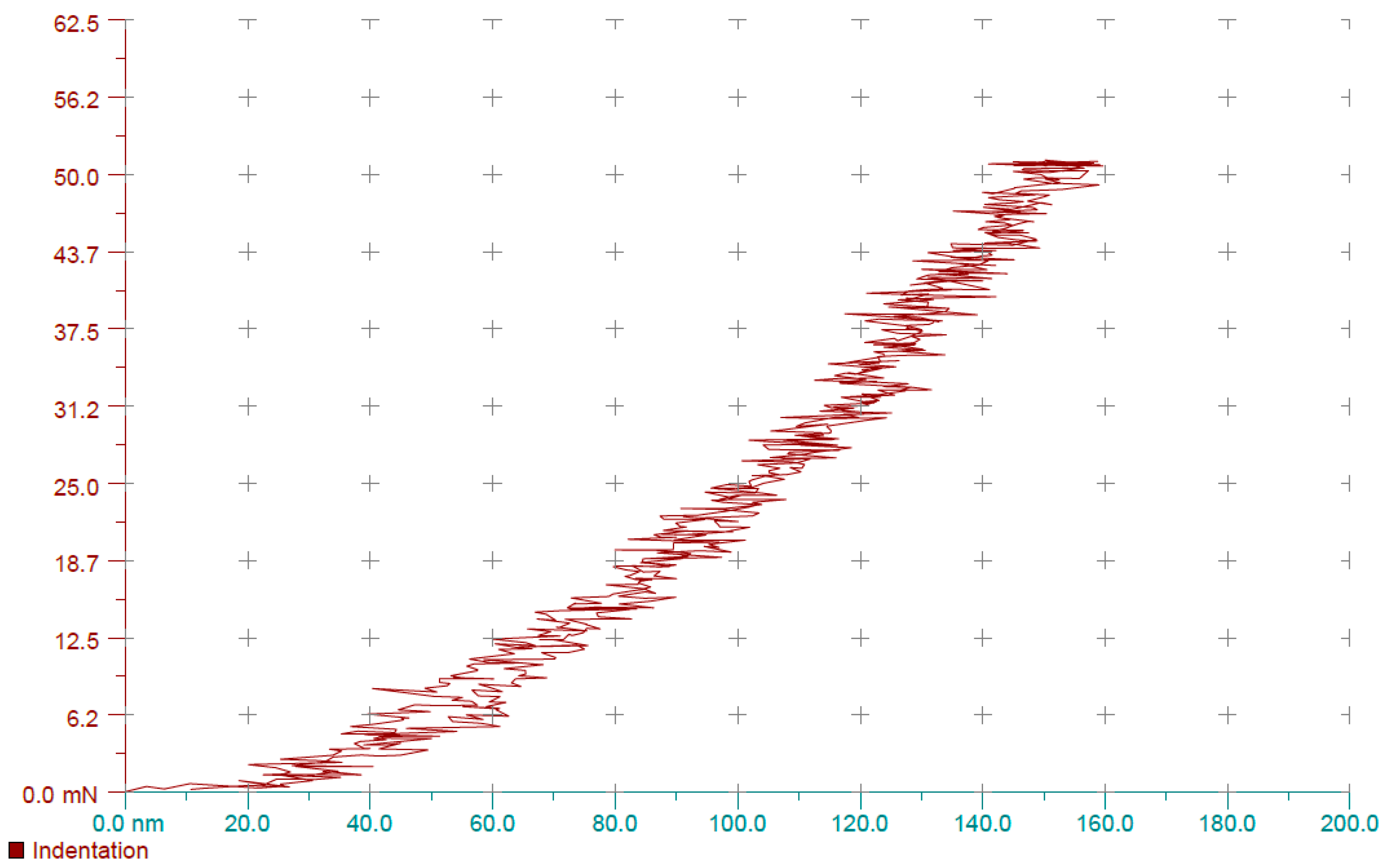
3.2. The Hardness and Elastic Modulus

We obtained values of hardness in the range from 62 to 117 GPa and elastic modulus in the range from 914 to 1099 GPa. A typical loading–unloading curve is represented in Figure 10.
From the presented load–unloading curve, we identified the following characteristics:
-
hardness 62.8 GPa;
-
elastic modulus 914.6 GPa;
-
indenter penetration depth 155.816 nm.
We qualified the optimal mode for the synthesis of heavily boron-doped diamond:
-
temperature 1100 °C;
-
H2 flow rate 480 cm3/min;
-
CH4 flow rate 25 cm3/min;
-
H2 – (C2H5O)3B flow rate 10 cm3/min;
-
microwave power 3800 W;
-
reactor pressure 9.806 kPa.
The obtained experimental data allow further experiments to reduce the boron concentration in single-crystal diamond film and to introduce more oxygen to etch the surface during the deposition process of thick homogeneous boron-doped diamond layers.

4. Conclusions

The paper presents a scheme of boron-doped diamond CVD synthesis by using triethyl borate as a boron-containing substance. The replacement of the boron-containing substance from diborane to triethyl borate allowed etching, creating polycrystalline diamond via an all-synthesis process without the need for interruption due to oxygen atoms from triethyl borate. The high boron content obtained according to the proposed scheme samples (2.9% mass) is explained by the need for high oxygen atoms concentration in the gas mixture for successful etching of the emerging polycrystalline diamond. As a result of synthesis, it is possible to obtain boron-doped diamond with a stable boron distribution in the volume.
Using the Oliver–Farr method, we measured the hardness and elastic modulus of obtained coatings, varying from 62 to 117 and 914 to 1099 GPa, respectively.
In the future, work will be developed in the direction of reducing the concentration of triethyl borate in the gas mixture and optimizing parameters for sectoral growth in order to obtain doped diamond layers. Compensation of oxygen atoms will be realized through direct oxygen supply to the gas mixture, which is stable in contrast to diborane.

Author Contributions

Conceptualization, N.I.P. and B.V.S.; methodology, A.I.L., A.E.A., and A.M.P.; validation, A.E.A., A.L.M., and A.M.P.; formal analysis, A.I.L. and A.L.M.; investigation, N.I.P., B.V.S., A.E.A., and T.V.M.; resources, N.I.P.; data curation, N.I.P.; writing—original draft preparation, A.L.M. and T.V.M.; writing—review and editing, A.L.M. and T.V.M.; visualization, T.V.M.; supervision, B.V.S.; project administration, N.I.P.; funding acquisition, N.I.P. All authors have read and agreed to the published version of the manuscript.

Funding

This research was funded by the Ministry of Education and Science of the Russian Federation, grant number 075-15-2019-255, dated 9 July 2019, a unique identifier of the agreement RFMEFI57818X0266.

Conflicts of Interest

The authors declare no conflict of interest.

References

  1. Jia, F.; Bai, Y.; Qu, F.; Zhao, J.-J.; Zhuang, C.; Jiang, X. Effect of B/C ratio on the physical properties of highly boron-doped diamond films. Vacuum 2010, 84, 930–934. [Google Scholar] [CrossRef]
  2. Rehacek, V.; Hotový, I.; Marton, M.; Mikolasek, M.; Michniak, P.; Vincze, A.; Kromka, A.; Vojs, M. Voltammetric characterization of boron-doped diamond electrodes for electroanalytical applications. J. Electroanal. Chem. 2020, 862, 114020. [Google Scholar] [CrossRef]
  3. Zhang, J.; Yu, X.; Zhang, Z.-Q.; Zhao, Z.-Y. Preparation of boron-doped diamond foam film for supercapacitor applications. Appl. Surf. Sci. 2020, 506, 144645. [Google Scholar] [CrossRef]
  4. Tarelkin, S.; Bormashov, V.; Pavlov, S.; Kamenskyi, D.; Kuznetsov, M.; Terentiev, S.; Prikhodko, D.; Galkin, A.; Hubers, H.-W.; Blank, V. Evidence of linear Zeeman effect for infrared intracenter transitions in boron doped diamond in high magnetic fields. Diam. Relat. Mater. 2017, 75, 52–57. [Google Scholar] [CrossRef]
  5. Ficek, M.; Sobaszek, M.; Gnyba, M.; Ryl, J.; Gołuński, Ł.; Śmietana, M.; Jasiński, J.; Caban, P.; Bogdanowicz, R. Optical and electrical properties of boron doped diamond thin conductive films deposited on fused silica glass substrates. Appl. Surf. Sci. 2016, 387, 846–856. [Google Scholar] [CrossRef]
  6. Bormashov, V.; Tarelkin, S.; Buga, S.; Kuznetsov, M.; Terentiev, S.; Semenov, A.; Blank, V. Electrical properties of the high quality boron-doped synthetic single-crystal diamonds grown by the temperature gradient method. Diam. Relat. Mater. 2013, 35, 19–23. [Google Scholar] [CrossRef]
  7. Mortet, V.; Pernot, J.; Jomard, F.; Soltani, A.; Remes, Z.; Barjon, J.; D’Haen, J.; Haenen, K. Properties of boron-doped epitaxial diamond layers grown on (110) oriented single crystal substrates. Diam. Relat. Mater. 2015, 53, 29–34. [Google Scholar] [CrossRef]
  8. Bolshakov, A.; Zyablyuk, K.; Kolyubin, V.; Dravin, V.; Khmelnitskii, R.; Nedosekin, P.; Pashentsev, V.; Tyurin, E.; Ralchenko, V. Thin CVD diamond film detector for slow neutrons with buried graphitic electrode. Nucl. Instrum. Methods Phys. Res. Sect. A 2017, 871, 142–147. [Google Scholar] [CrossRef]
  9. Halliwell, S.; May, P.; Fox, N.; Othman, M. Investigations of the co-doping of boron and lithium into CVD diamond thin films. Diam. Relat. Mater. 2017, 76, 115–122. [Google Scholar] [CrossRef] [Green Version]
  10. Ohmagari, S.; Srimongkon, K.; Yamada, H.; Umezawa, H.; Tsubouchi, N.; Chayahara, A.; Shikata, S.; Mokuno, Y. Low resistivity p+ diamond (100) films fabricated by hot-filament chemical vapor deposition. Diam. Relat. Mater. 2015, 58, 110–114. [Google Scholar] [CrossRef]
  11. Demlow, S.N.; Rechenberg, R.; Grotjohn, T.; Nicley, S.S. The effect of substrate temperature and growth rate on the doping efficiency of single crystal boron doped diamond. Diam. Relat. Mater. 2014, 49, 19–24. [Google Scholar] [CrossRef] [Green Version]
  12. Tallaire, A.; Achard, J.; Silva, F.; Sussmann, R.S.; Gicquel, A.; Rzepka, E. Oxygen plasma pre-treatments for high quality homoepitaxial CVD diamond deposition. Phys. Status Solidi 2004, 201, 2419–2424. [Google Scholar] [CrossRef]
  13. Chen, C.-F.; Chen, S.-H.; Hong, T.-M.; Wang, T.-C. Boron-doped diamond films using trimethylborate as a dopant source in methane-carbon dioxide gas mixtures. Diam. Relat. Mater. 1994, 3, 632–637. [Google Scholar] [CrossRef]
  14. Okushi, H. High quality homoepitaxial CVD diamond for electronic devices. Diam. Relat. Mater. 2001, 10, 281–288. [Google Scholar] [CrossRef]
  15. Arima, K.; Miyatake, H.; Teraji, T.; Ito, T. Effects of vicinal angles from (001) surface on the Boron-doping features of high-quality homoepitaxial diamond films grown by the high-power microwave plasma chemical-vapor-deposition method. J. Cryst. Growth 2007, 309, 145–152. [Google Scholar] [CrossRef]
  16. Teraji, T.; Wada, H.; Yamamoto, M.; Arima, K.; Ito, T. Highly efficient doping of boron into high-quality homoepitaxial diamond films. Diam. Relat. Mater. 2006, 15, 602–606. [Google Scholar] [CrossRef]
  17. Volpe, P.-N.; Arnault, J.-C.; Tranchant, N.; Chicot, G.; Pernot, J.; Jomard, F.; Bergonzo, P. Boron incorporation issues in diamond when TMB is used as precursor: Toward extreme doping levels. Diam. Relat. Mater. 2012, 22, 136–141. [Google Scholar] [CrossRef]
  18. Issaoui, R.; Achard, J.; Silva, F.; Tallaire, A.; Tardieu, A.; Gicquel, A.; Pinault, M.A.; Jomard, F. Growth of thick heavily boron-doped diamond single crystals: Effect of microwave power density. Appl. Phys. Lett. 2010, 97, 182101. [Google Scholar] [CrossRef]
  19. De Feudis, M.; Mille, V.; Valentin, A.; Brinza, O.; Tallaire, A.; Tardieu, A.; Issaoui, R.; Achard, J. Ohmic graphite-metal contacts on oxygen-terminated lightly boron-doped CVD monocrystalline diamond. Diam. Relat. Mater. 2019, 92, 18–24. [Google Scholar] [CrossRef]
  20. Tallaire, A.; Valentin, A.; Mille, V.; William, L.; Pinault-Thaury, M.; Jomard, F.; Barjon, J.; Achard, J. Growth of thick and heavily boron-doped (113)-oriented CVD diamond films. Diam. Relat. Mater. 2016, 66, 61–66. [Google Scholar] [CrossRef]
  21. Barjon, J.; Chikoidze, E.; Jomard, F.; Dumont, Y.; Pinault-Thaury, M.-A.; Issaoui, R.; Brinza, O.; Achard, J.; Silva, F. Homoepitaxial boron-doped diamond with very low compensation. Phys. Status Solidi 2012, 209, 1750–1753. [Google Scholar] [CrossRef]
  22. Dorsch, O.; Holzner, K.; Werner, M.; Obermeier, E.; Harper, R.; Johnston, C.; Chalker, P.R.; Buckley-Golder, I. Piezoresistive effect of boron-doped diamond thin films. Diam. Relat. Mater. 1993, 2, 1096–1099. [Google Scholar] [CrossRef]
  23. Zubkov, V.; Kucherova, O.V.; Bogdanov, S.A.; Zubkova, A.V.; Butler, J.; Ilyin, V.; Afanas’Ev, A.V.; Vikharev, A.L. Temperature admittance spectroscopy of boron doped chemical vapor deposition diamond. J. Appl. Phys. 2015, 118, 145703. [Google Scholar] [CrossRef]
  24. Bogdanov, S.; Vikharev, A.; Drozdov, M.; Radishev, D. Synthesis of thick and high-quality homoepitaxial diamond with high boron doping level: Oxygen effect. Diam. Relat. Mater. 2017, 74, 59–64. [Google Scholar] [CrossRef]
  25. Jiang, X.; Willich, P.; Paul, M.; Klages, C.-P. In situ boron doping of chemical-vapor-deposited diamond films. J. Mater. Res. 1999, 14, 3211–3220. [Google Scholar] [CrossRef]
  26. Srikanth, V.V.S.S.; Kumar, P.S.; Kumar, V.B. A Brief Review on the In Situ Synthesis of Boron-Doped Diamond Thin Films. Int. J. Electrochem. 2012, 2012, 218393. [Google Scholar] [CrossRef] [Green Version]
  27. Yap, C.; Ansari, K.; Xiao, S.; Yee, S.; Chukka, R.; Misra, D. Properties of near-colourless lightly boron doped CVD diamond. Diam. Relat. Mater. 2018, 88, 118–122. [Google Scholar] [CrossRef]
  28. National Library of Medicine National Center for Biotechnology Information. Boranes. Available online: https://pubchem.ncbi.nlm.nih.gov/compound/Diborane (accessed on 29 April 2020).
  29. National Research Council. Acute Exposure Guideline Levels for Selected Airborne Chemicals; National Academies Press: Washington, DC, USA, 2003; Volume 3, p. 4. [Google Scholar]
  30. Pan, L.; Lew, K.-K.; Redwing, J.M.; Dickey, E.C. Effect of diborane on the microstructure of boron-doped silicon nanowires. J. Cryst. Growth 2005, 277, 428–436. [Google Scholar] [CrossRef]
  31. Gandía, J.; Cárabe, J.; Swinnen, J. A simple diborane-degradation model for controlling p-type doping of microcrystalline silicon. Sol. Energy Mater. Sol. Cells 2002, 73, 75–90. [Google Scholar] [CrossRef]
  32. Rojwal, V.; Singha, M.K.; Mondal, T.; Mondal, D. Formation of micro structured doped and undoped hydrogenated silicon thin films. Superlattices Microstruct. 2018, 124, 201–217. [Google Scholar] [CrossRef]
  33. Kim, C.-H.; Jung, S.-H.; Jeon, J.-H.; Han, M.-K. A simple low-temperature laser-doping employing phosphosilicate glass and borosilicate glass films for the source and drain formation in poly-Si thin film transistors. Thin Solid Films 2001, 397, 4–7. [Google Scholar] [CrossRef]
  34. Lottspeich, F.; Müller, M.; Köhler, R.; Fischer, G.; Schneiderlöchner, E.; Palinginis, P. Influence of nitride and nitridation on the doping properties of PECVD-deposited BSG layers. Energy Procedia 2017, 124, 691–699. [Google Scholar] [CrossRef]
  35. Mikhailov, B.M. The Chemistry of Diborane. Russ. Chem. Rev. 1962, 31, 207–224. [Google Scholar] [CrossRef]
  36. Kauffman, G.B. ENCYCLOPÆDIA BRITANNICA. Borane. Available online: https://www.britannica.com/science/borane (accessed on 29 April 2020).
  37. Cotton, F.A.; Wilkinson, G.; Gaus, P.L. Chemia Nieorganiczna; Wydawnictwo Naukowe: Warszawa, Poland, 1995. [Google Scholar]
  38. Docks, E.L. Boric Acid Esters; Wiley: Hoboken, NJ, USA, 2000. [Google Scholar]
  39. Ast, J.; Ghidelli, M.; Durst, K.; Göken, M.; Sebastiani, M.; Korsunsky, A.M.; Goeken, M. A review of experimental approaches to fracture toughness evaluation at the micro-scale. Mater. Des. 2019, 173, 107762. [Google Scholar] [CrossRef]
  40. Ghidelli, M.; Sebastiani, M.; Collet, C.; Guillemet, R. Determination of the elastic moduli and residual stresses of freestanding Au-TiW bilayer thin films by nanoindentation. Mater. Des. 2016, 106, 436–445. [Google Scholar] [CrossRef]
  41. Moshchenok, V.I.; Lyakhovitsky, M.M.; Doshechkina, I.V.; Kukhareva, I.E. Comparison of the calculation method for assessing the surface nano- and microhardness of materials with the Oliver-Farr method. Metals 2009, 8, 719. [Google Scholar]
  42. Man, W.; Wang, J.; Wang, C.; Wang, S.; Xiong, L. Planarizing CVD diamond films by using hydrogen plasma etching enhanced carbon diffusion process. Diam. Relat. Mater. 2007, 16, 1455–1458. [Google Scholar] [CrossRef]
  43. Enlund, J.; Isberg, J.; Karlsson, M.; Nikolajeff, F.; Olsson, J.; Twitchen, D.J. Anisotropic dry etching of boron doped single crystal CVD diamond. Carbon 2005, 43, 1839–1842. [Google Scholar] [CrossRef]
  44. Bolshakov, A.P.; Ralchenko, V.G.; Polsky, A.V.; Ashkinazi, E.E.; Homich, A.A.; Sharanov, G.V.; Hmelnitsky, R.A.; Zavedeev, E.V.; Homich, A.V.; Sovik, D.N. Synthys single crystal diamond in microwave plasma. Prikladnaya Fizika 2011, 6, 104–110. [Google Scholar]
  45. Spitsyn, B.V.; Aleksenko, A.E. Chemical crystallization of diamond and deposition diamond coating from the gas phase. Met. Prot. 2007, 5, 456–474. [Google Scholar] [CrossRef]
Figure 1. The surface of large thickness diamond with defects on the surface and facets (substrate size—5 × 5 × 0.5 mm, deposited diamond layer thickness—0.5 mm).
Processes 08 00666 g001
Figure 2. Scheme of loading–unloading curve.
Processes 08 00666 g002
Figure 3. Schematic diagram of the technology of preparing single-crystal diamond substrates for doping and the doping process itself.
Processes 08 00666 g003
Figure 4. Boron-doped diamond samples (Sample 1—left, Sample 2—right).
Processes 08 00666 g004
Figure 5. SEM images of the sample surfaces. (a) Sample 1, (b) Sample 2.
Processes 08 00666 g005
Figure 6. SEM image of Sample 1 with areas for identifying surface composition.
Processes 08 00666 g006
Figure 7. EDS analysis of sample 1.
Processes 08 00666 g007aProcesses 08 00666 g007b
Figure 8. Areas for identifying Sample 2 surface composition.
Processes 08 00666 g008
Figure 9. EDS analysis of Sample 2.
Processes 08 00666 g009
Figure 10. Loading–unloading curve.
Processes 08 00666 g010
Table 1. Frequently used doping diamond boron-containing substances.
SubstanceCoating Thickness, μmReferences
B(CH3)31.5–25[14,15,16,17]
B2H65–350[18,19,20,21]
BCl30.5–1.0[22]
(CH3O)3B2–>100[23,24]
(C2H5O)3B[25,26]
hBN770–1020[27]
Table 2. Some characteristics of the most important boranes [33].
CompoundThermal StabilityBehavior on AirReaction with H2O
B2H6Stable
at 25 °C
Self-ignitesHydrolyzes immediately
B4H10Unstable
at 25 °C
Self-ignites in the presence of waterHydrolyzes
B5H9Stable at 25 °CSelf-ignitesHydrolyzes by heating
B5H11Unstable
at 150 °C and above
Self-ignitesHydrolyzes rapidly
B6H10Unstable
at 25 °C
StableHydrolyzes by heating
B6H12Unstable
at 25 °C
StableHydrolyzes by heating
B9H15Unstable
at 25 °C
StableHydrolyzes by heating
B10H14Stable at 150 °CExtremely stableHydrolyzes slowly
Table 3. Sample 1 elemental analysis.
The Number of AreaCBO
197.12.9
297.22.8
392.23.24.6
494.13.42.5
Table 4. Sample 2 elemental analysis.
The Number of AreaCBO
597.12.9
694.12.53.4
794.13.42.5

