
Analysis of a Series‑Parallel Resonant Converter for DC Microgrid Applications

Abstract
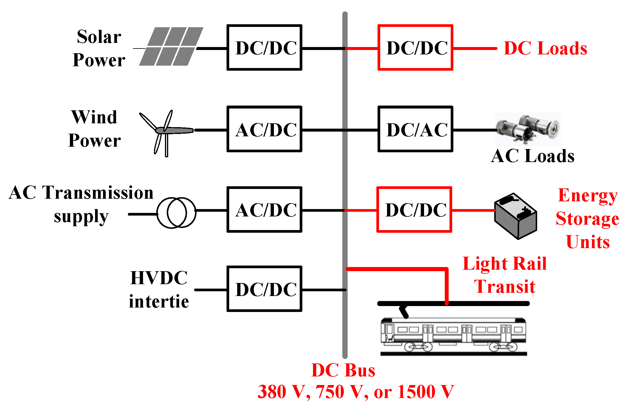
:1. Introduction
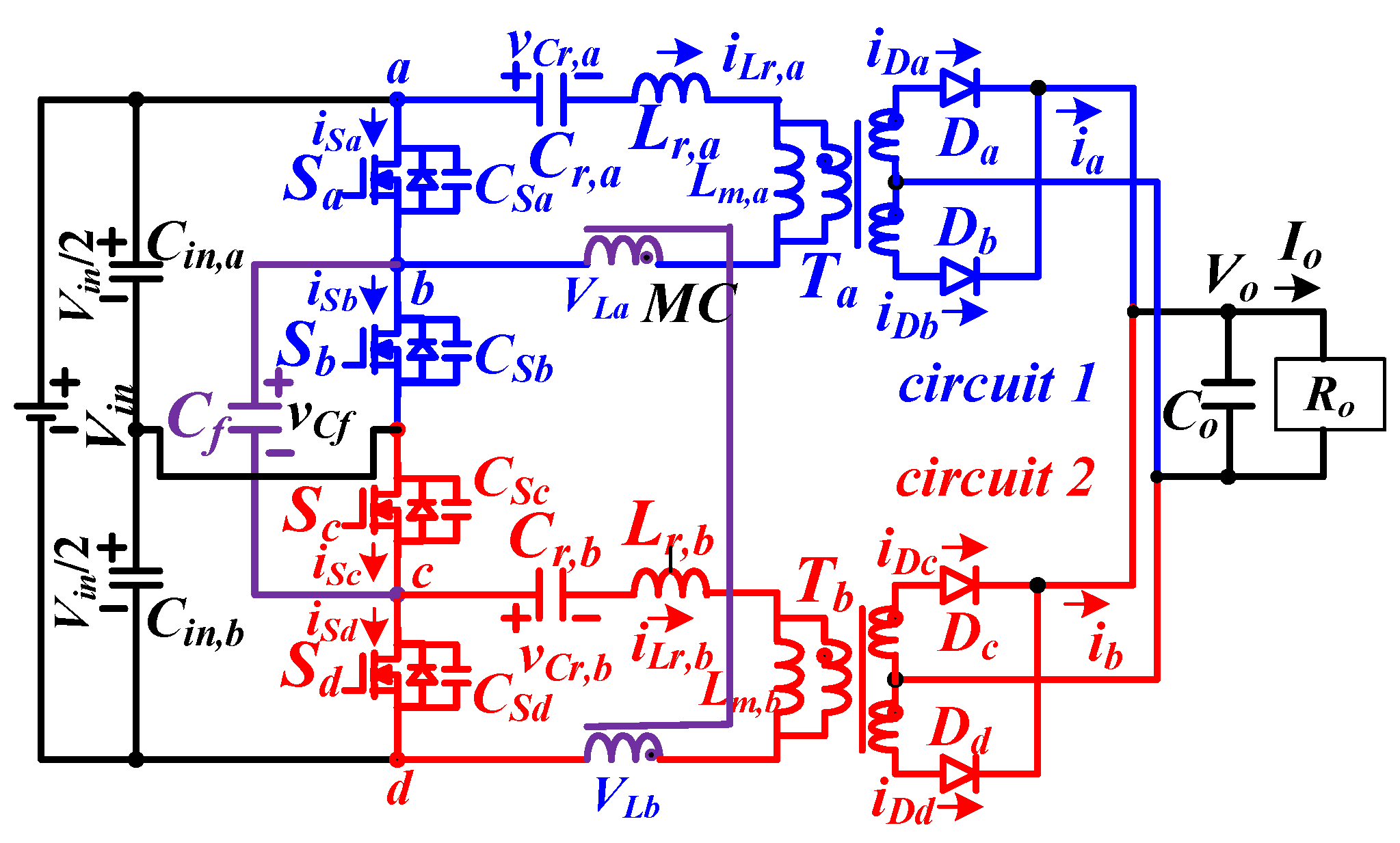
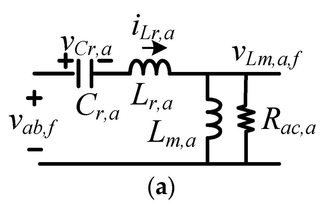
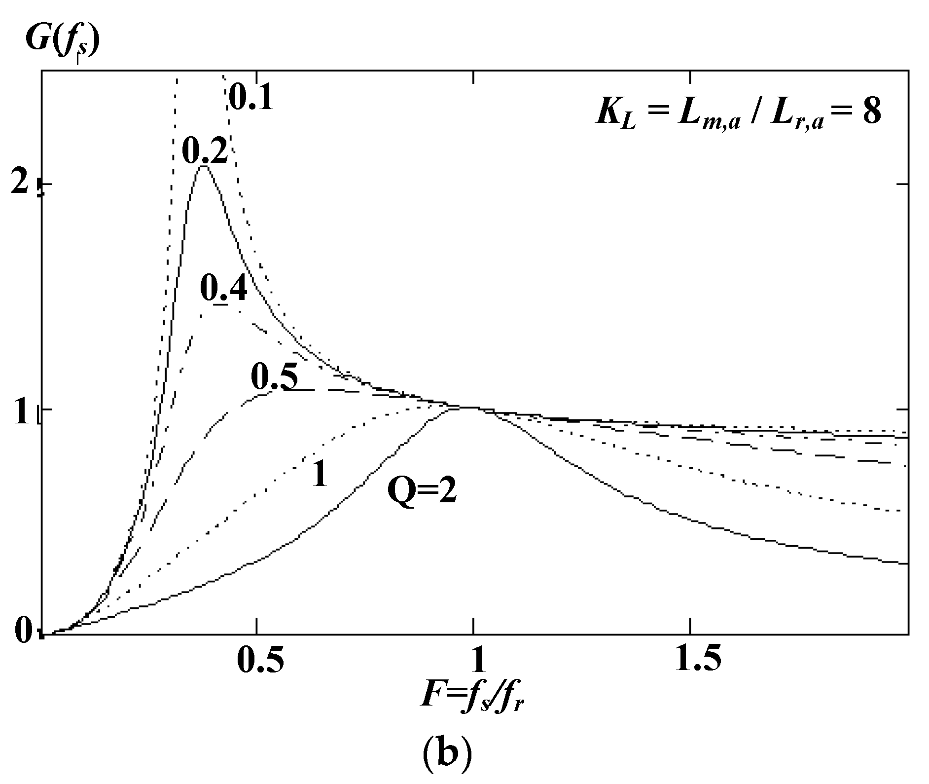
2. Presented Resonant Converter
2.1. Circuit Characteristics of a Conventional Resonant Converter
2.2. Proposed LLC Resonant Converter
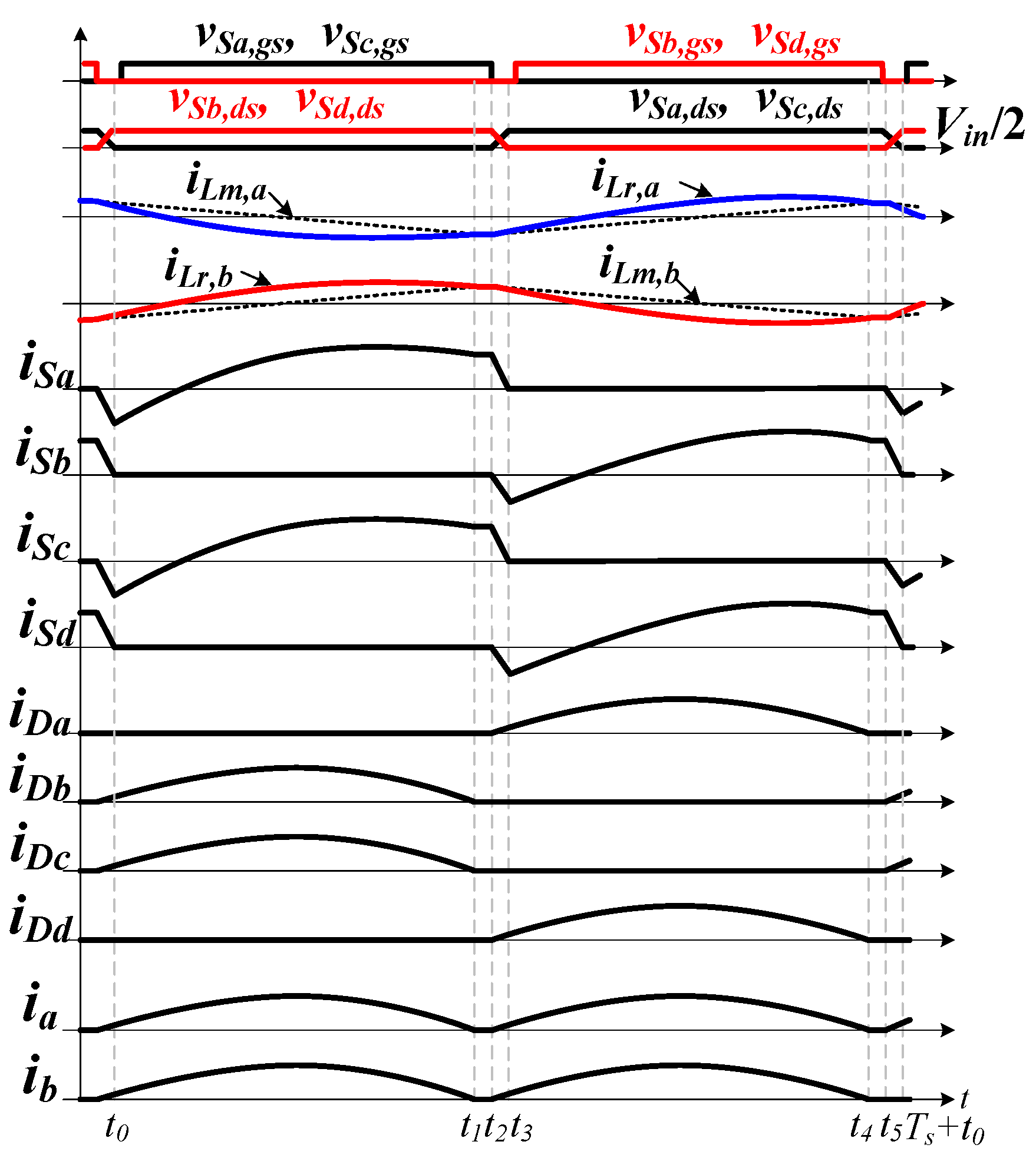
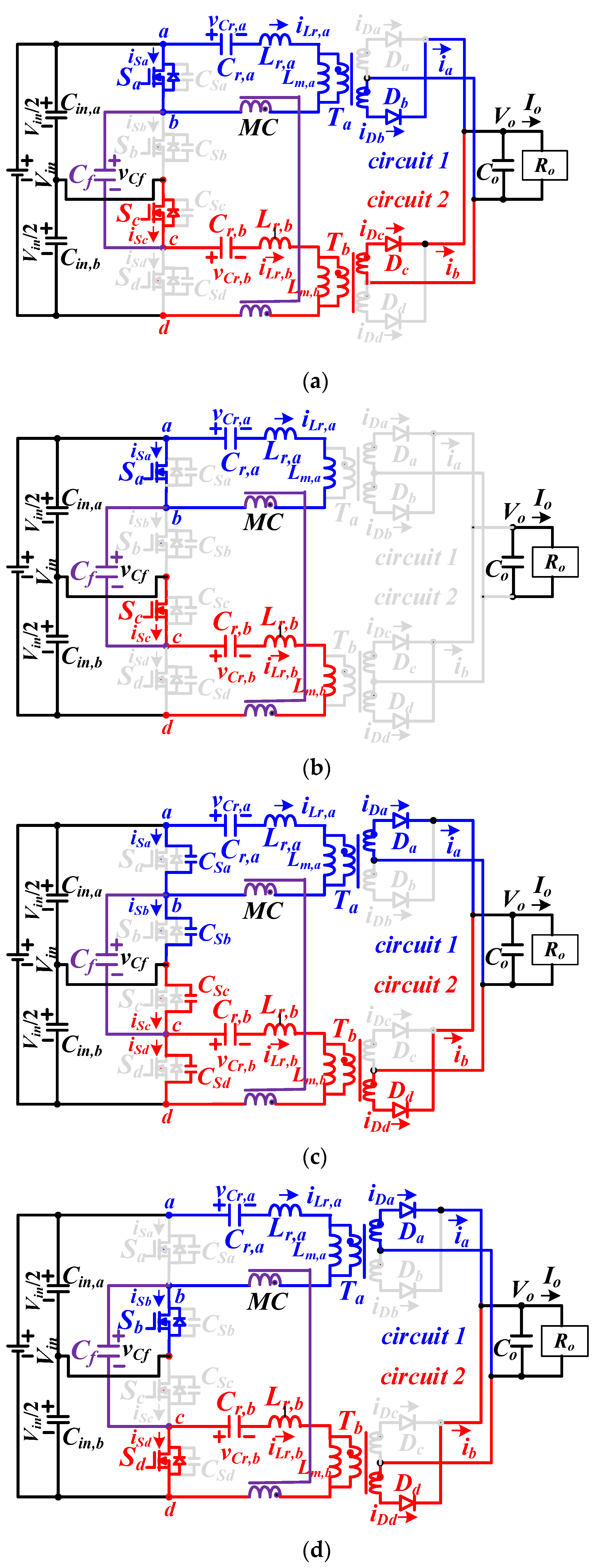
3. Principle of Operation
- (1)
- Transformers Ta and Tb have identical turn-ratio na = nb = np/ns;
- (2)
- Inductances Lm,a = Lm,b = Lm and Lr,a = Lr,b = Lr;
- (3)
- Sa~Sc have identical output capacitances CSa = CSb = CSc = CSd = CS;
- (4)
- Capacitances Cin,a = Cin,b and Cr,a = Cr,b = Cr.
4. System Analysis and Design Example
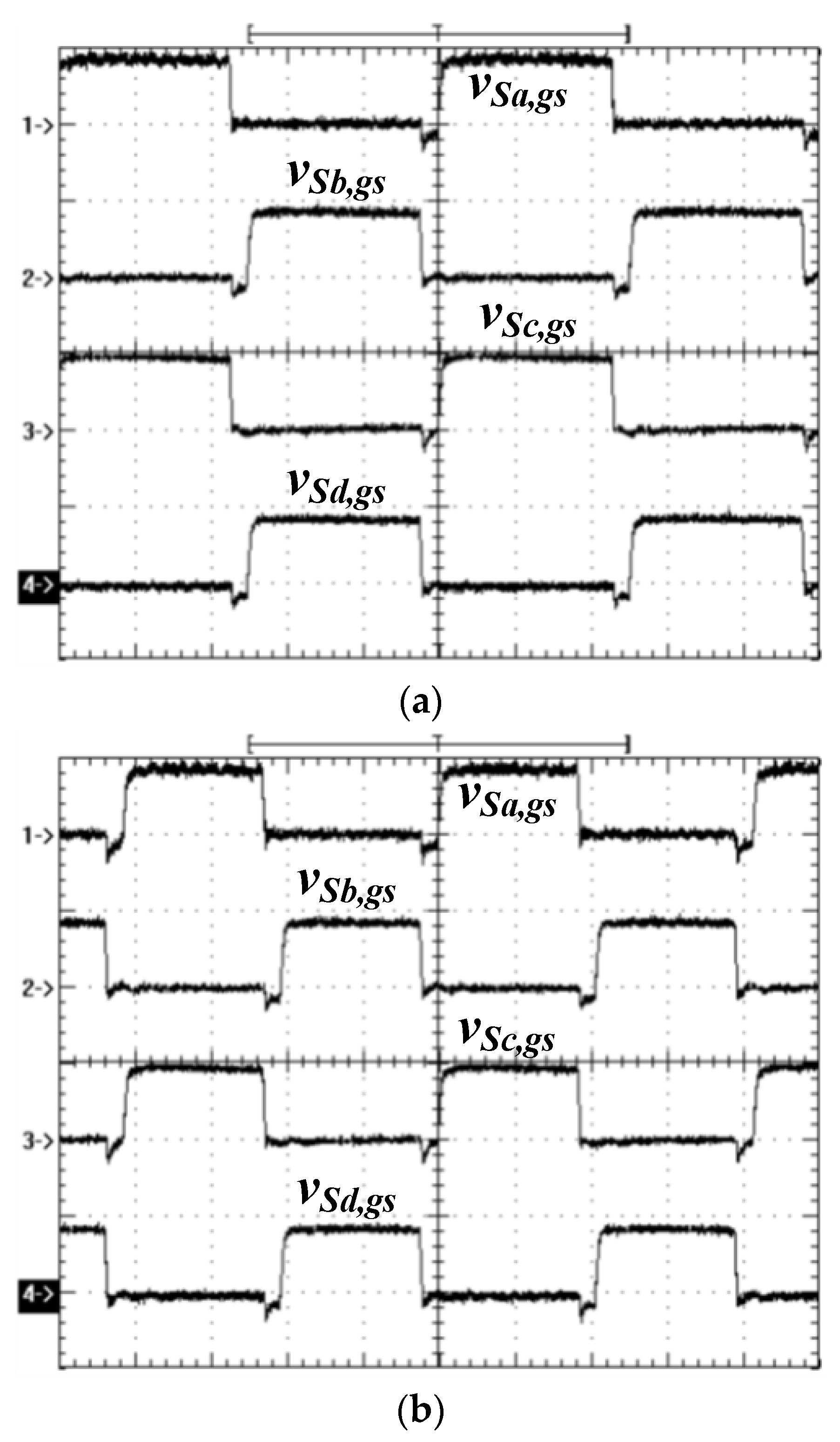
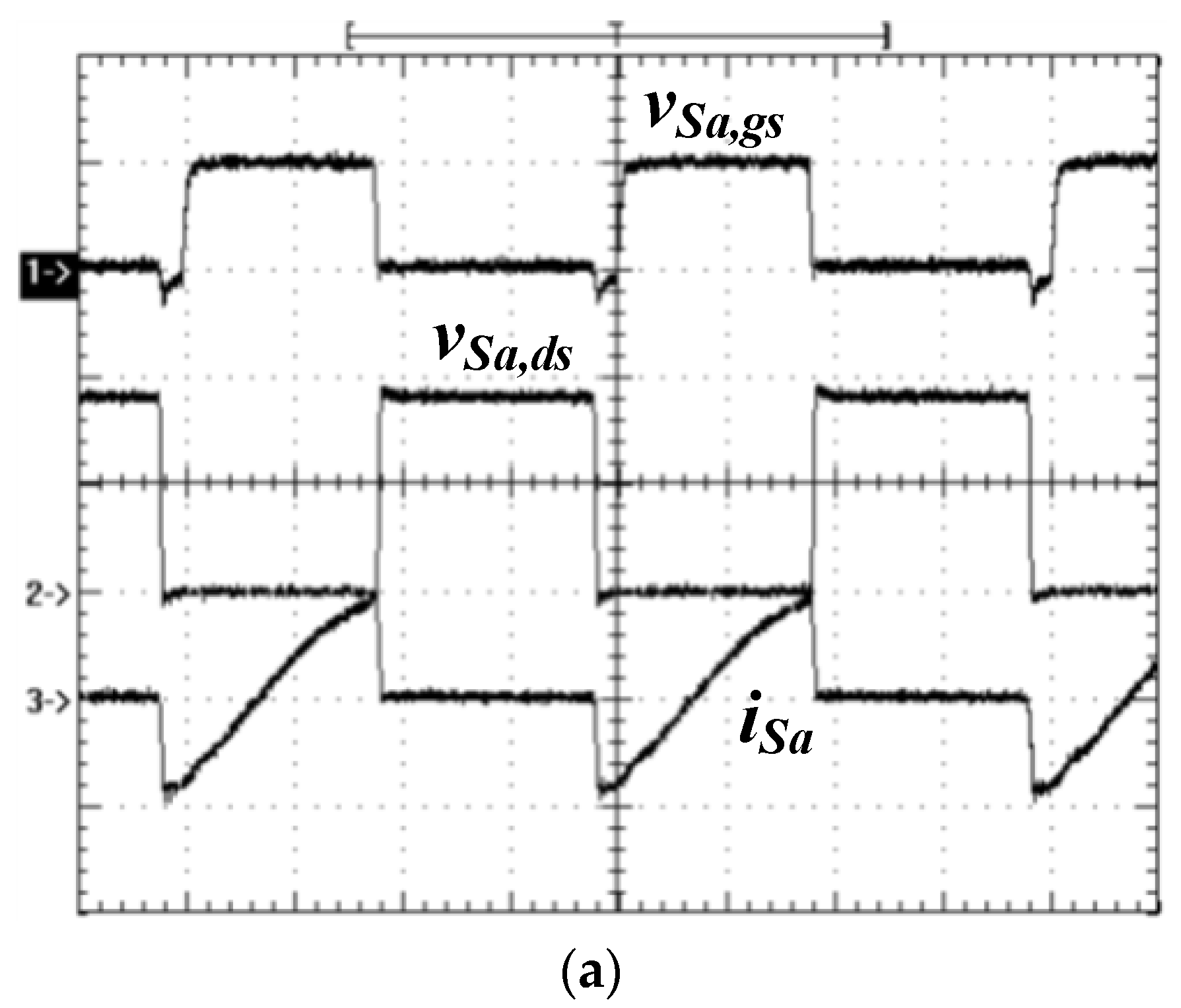
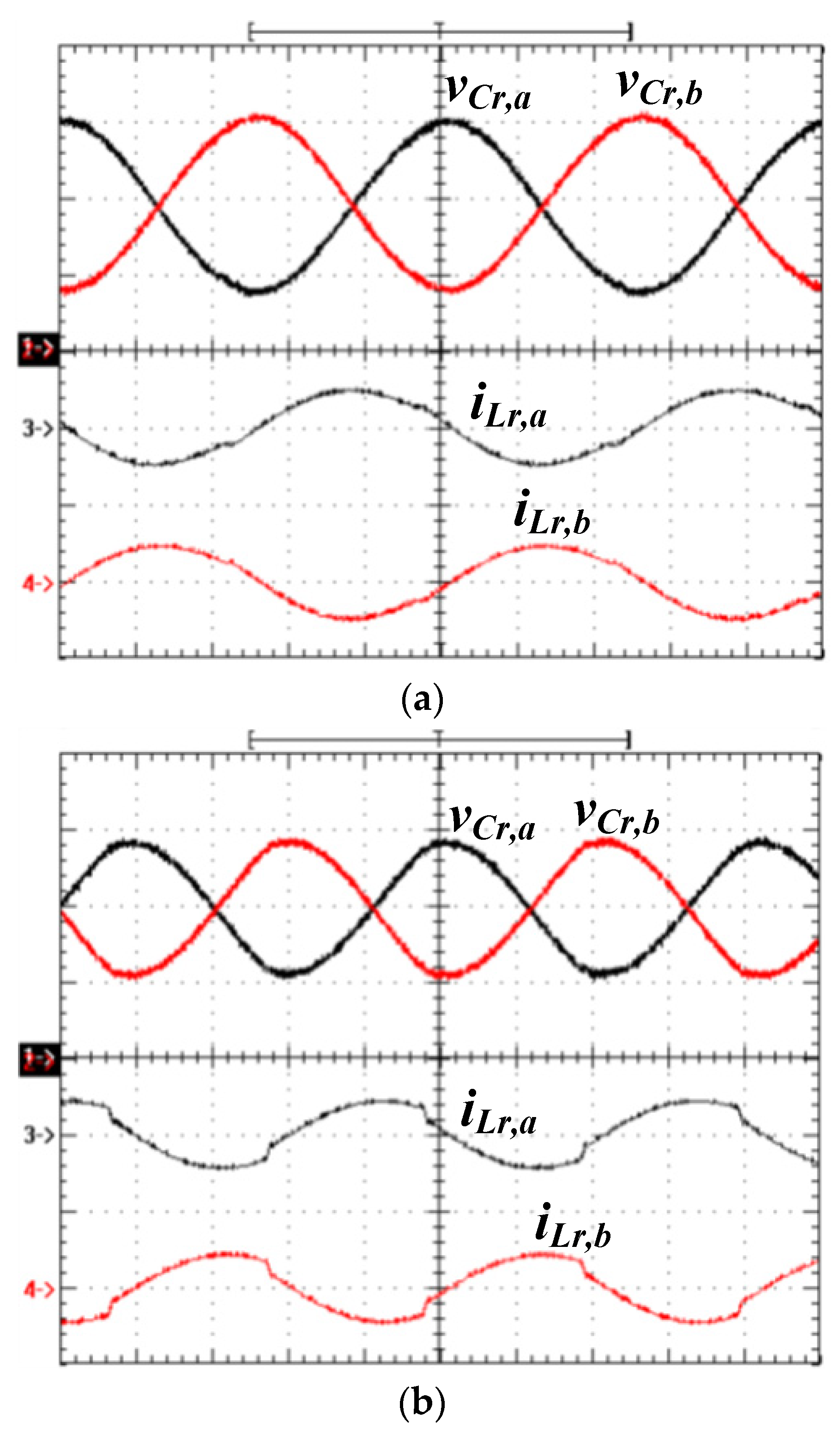
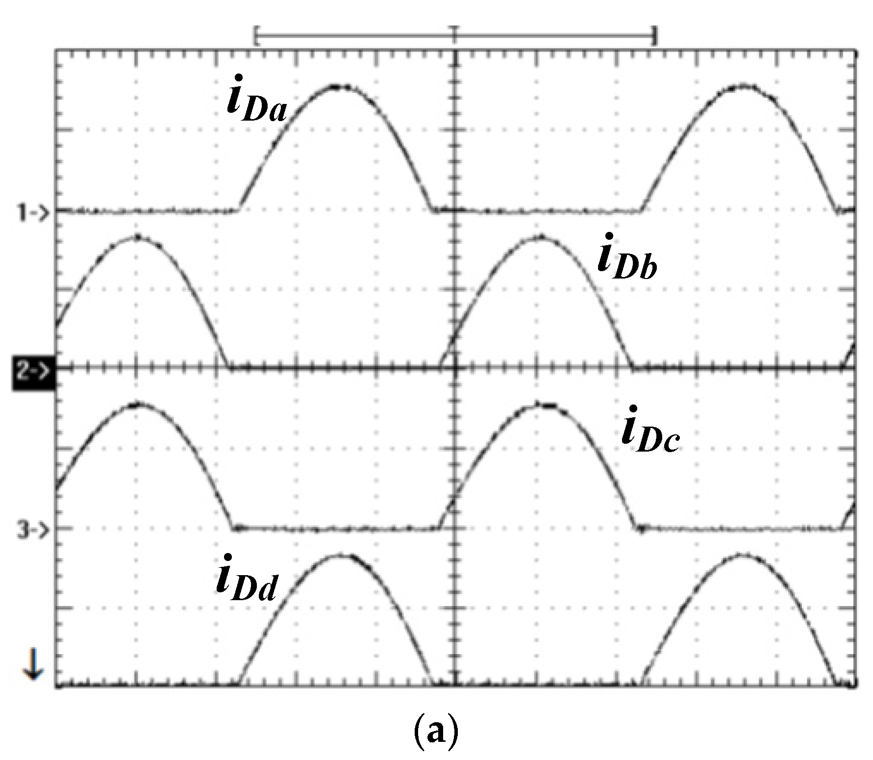
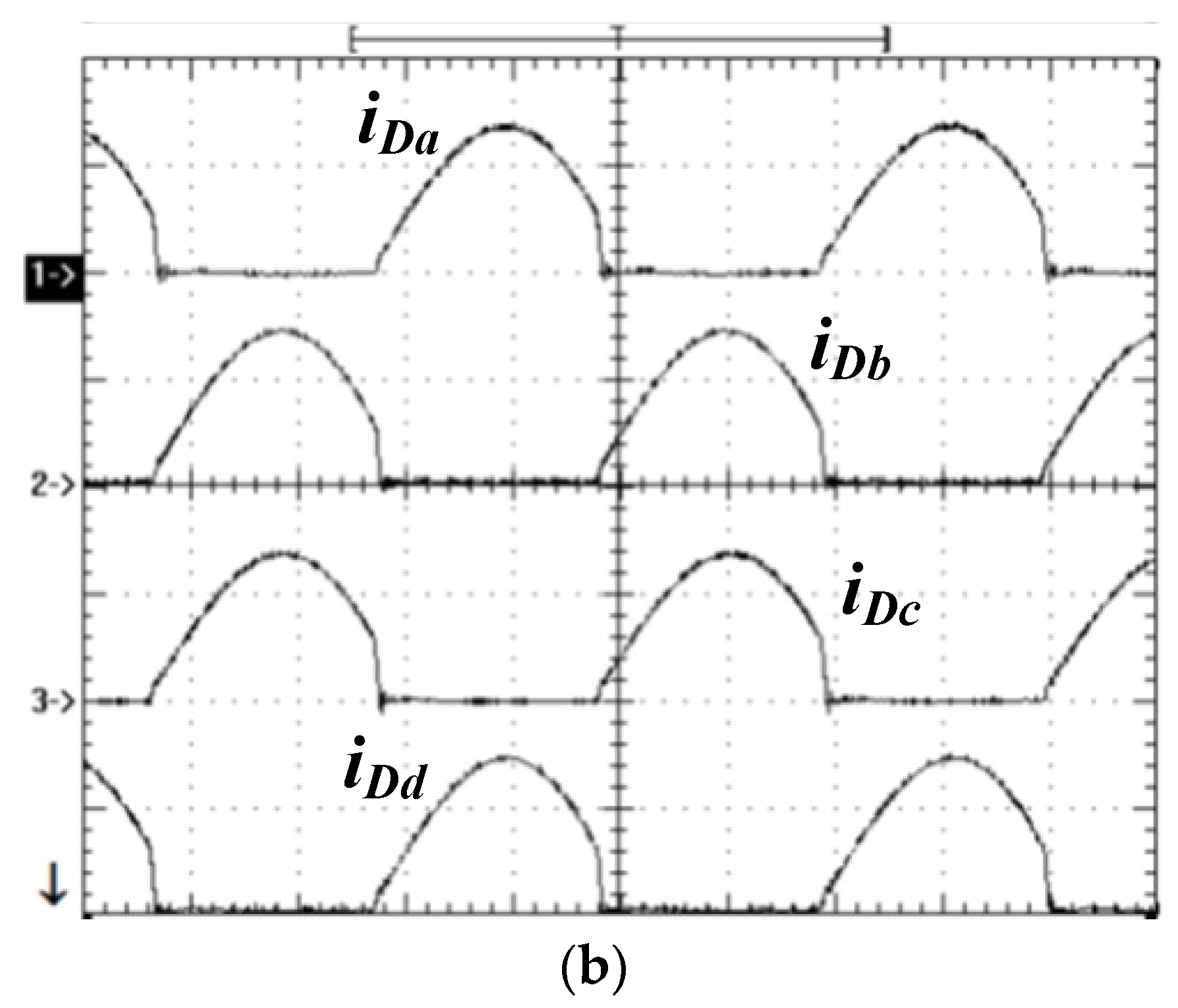
5. Experimental Results
6. Conclusions
Funding
Acknowledgments
Conflicts of Interest
References
- Song, B.M.; McDowell, R.; Bushnell, A.; Ennis, J. A three-level dc–dc converter with wide-input voltage operation for ship-electric power-distribution systems. IEEE Trans. Plasma Sci. 2004, 32, 1856–1863. [Google Scholar] [CrossRef]
- Fu, D.X.; Lee, F.C.; Qiu, Y.; Wang, F. A novel high-power-density three-level LCC resonant converter with constant-power-factor-control for charging applications. IEEE Trans. Power Electron. 2008, 23, 2411–2420. [Google Scholar] [CrossRef]
- Dragicevic, T.; Lu, X.; Vasquez, J.C.; Guerrero, J.M. DC microgrids—Part I: A review of control strategies and stabilization techniques. IEEE Trans. Power Electron. 2016, 31, 4876–4891. [Google Scholar] [CrossRef] [Green Version]
- Dragicevic, T.; Lu, X.; Vasquez, J.C.; Guerrero, J.M. DC microgrids—Part II: A review of power architectures, applications, and standardization issue. IEEE Trans. Power Electron. 2016, 31, 3528–3549. [Google Scholar] [CrossRef] [Green Version]
- Chua, T.Z.Y.; Ong, Y.T.; Toh, C.L. Transformerless DC traction power conversion system design for light-rail-transit (LRT). In Proceedings of the IEEE Conference on Energy Conversion (CENCON), Kuala Lumpur, Malaysia, 30–31 October 2017; pp. 38–43. [Google Scholar]
- Akagi, H. Classification, terminology, and application of the modular multilevel cascade converter (MMCC). IEEE Trans. Power Electron. 2011, 26, 3119–3130. [Google Scholar] [CrossRef]
- Lee, J.P.; Min, B.D.; Kim, T.J.; Yoo, D.W.; Yoo, J.Y. Input-Series-Output-Parallel Connected DC/DC Converter for a Photovoltaic PCS with High Efficiency under a Wide Load Range. J. Power Electron. 2010, 10, 9–13. [Google Scholar] [CrossRef]
- Tao, X.; Li, Y.; Sun, M. A pi-based control scheme for primary cascaded H-bridge rectifier in transformerless traction converters. In Proceedings of the International Conference on Electrical Machines and Systems (ICEMS), Incheon, Korea, 10–13 October 2010; pp. 824–828. [Google Scholar]
- Ji, S.; Lu, T.; Zgao, Z.; Yu, H.; Yuan, L. Series-connected HV-IGBTs using active voltage balancing control with status feedback circuit. IEEE Trans. Power Electron. 2015, 30, 4165–4174. [Google Scholar] [CrossRef]
- Lim, T.C.; Williams, B.W.; Finney, S.J.; Palmer, P.R. Series-connected IGBTs using active voltage control technique. IEEE Trans. Power Electron. 2013, 28, 4083–4103. [Google Scholar] [CrossRef]
- Chen, W.; Wang, G. Decentralized voltage-sharing control strategy for fully modular input-series-output-series system with improved voltage regulation. IEEE Trans. Ind. Electron. 2015, 62, 2777–2787. [Google Scholar] [CrossRef]
- Sha, D.; Deng, K.; Liao, X. Duty cycle exchanging control for input-series-output-series connected two PS-FB DC-DC converter. IEEE Trans. Power Electron. 2012, 27, 1490–1501. [Google Scholar] [CrossRef]
- Lin, B.R.; Cheng, P.J. New ZVS DC-DC converter with series-connected transformers to balance the output currents. IEEE Trans. Power Electron. 2014, 29, 246–255. [Google Scholar] [CrossRef]
- Ertl, H.; Kolar, J.W.; Zach, F.C. A novel multicell DC-AC converter for applications in renewable energy systems. IEEE Trans. Ind. Electron. 2002, 49, 1048–1057. [Google Scholar] [CrossRef]
- Perez, M.A.; Bernet, S.; Rodriguez, J.; Kouro, S.; Lizana, R. Circuit topologies, modeling, control schemes, and applications of modular multilevel converters. IEEE Trans. Power Electron. 2015, 30, 4–17. [Google Scholar] [CrossRef]
- Akagi, H.; Kitada, R. Control and Design of a Modular Multilevel Cascade BTB System Using Bidirectional Isolated DC/DC Converters. IEEE Trans. Power Electron. 2011, 26, 2457–2464. [Google Scholar] [CrossRef]
- Nami, A.; Liang, J.; Dijkhuizen, F.; Demetriades, G.D. Modular multilevel converters for HVDC applications: Review on converter cells and functionalities. IEEE Trans. Power Electron. 2015, 30, 18–36. [Google Scholar] [CrossRef]
- Liu, W.; Jin, H.; Yao, W.; Lu, Z. An interleaved PWM method with voltage-balancing ability for half-bridge three-level converter. IEEE Trans. Power Electron. 2018, 33, 4594–4598. [Google Scholar] [CrossRef]
- Lin, B.R. Interleaved zero-voltage switching three-level converter with less output inductor counts. IET Proc. Power Electron. 2017, 10, 707–716. [Google Scholar] [CrossRef]
- Song, W.; Ma, J.; Zhou, L.; Feng, X. Deadbeat predictive power control of single-phase three-level neutral-point-clamped converters using space-vector modulation for electric railway traction. IEEE Trans. Power Electron. 2016, 31, 721–732. [Google Scholar] [CrossRef]
- Lin, B.R. Hybrid dc/dc converter based on dual three-level circuit and half-bridge circuit. IET Proc. Power Electron. 2016, 9, 817–824. [Google Scholar] [CrossRef]
- Dusmez, S.; Li, X.; Akin, B. A new multi input three-level dc/dc converter. IEEE Trans. Power Electron. 2016, 31, 1230–1240. [Google Scholar] [CrossRef]
- Haga, H.; Kurokawa, F. A novel modulation method of the full bridge three-level LLC resonant converter for battery charger of electrical vehicles. In Proceedings of the 2015 IEEE Energy Conversion Congress and Exposition, Montreal, QC, Canada, 20–24 September 2015; pp. 5498–5504. [Google Scholar]
- Liu, R.; Jones, E.A.; Wang, F.F.; Zhang, Z.; Costinett, D. Capacitor-clamped, three-level Gan-based dc-dc converter with dual voltage outputs for battery charger applications. IEEE J. Emerg. Sel. Top. Power Electron. 2016, 4, 841–853. [Google Scholar]
- Fu, D.; Liu, Y.; Lee, F.C.; Xu, M. A novel driving scheme for synchronous rectifiers in LLC resonant converters. IEEE Trans. Power Electron. 2009, 24, 1321–1329. [Google Scholar] [CrossRef]
- Gu, Y.; Lu, Z.; Hang, L.; Qian, Z.; Huang, G. Three-level LLC series resonant DC/DC converter. IEEE Trans. Power Electron. 2005, 20, 781–789. [Google Scholar] [CrossRef]
- Steigerwald, R.L. A comparison of half-bridge resonant converter topologies. IEEE Trans. Power Electron. 1988, 3, 174–182. [Google Scholar] [CrossRef]
- Liu, C.; Xu, X.; He, D.; Liu, H.; Tian, X.; Guo, Y.; Cai, G.; Ma, C.; Mu, G. Magnetic-coupling current-balancing cells based input-parallel output-parallel LLC resonant converter modules for high-frequency isolation of DC distribution systems. IEEE Trans. Power Electron. 2016, 31, 6968–6979. [Google Scholar] [CrossRef]


Publisher’s Note: MDPI stays neutral with regard to jurisdictional claims in published maps and institutional affiliations. |
© 2021 by the author. Licensee MDPI, Basel, Switzerland. This article is an open access article distributed under the terms and conditions of the Creative Commons Attribution (CC BY) license (http://creativecommons.org/licenses/by/4.0/).
Share and Cite
Lin, B.-R. Analysis of a Series‑Parallel Resonant Converter for DC Microgrid Applications. Processes 2021, 9, 542. https://doi.org/10.3390/pr9030542
Lin B-R. Analysis of a Series‑Parallel Resonant Converter for DC Microgrid Applications. Processes. 2021; 9(3):542. https://doi.org/10.3390/pr9030542
Chicago/Turabian StyleLin, Bor-Ren. 2021. "Analysis of a Series‑Parallel Resonant Converter for DC Microgrid Applications" Processes 9, no. 3: 542. https://doi.org/10.3390/pr9030542
APA StyleLin, B.-R. (2021). Analysis of a Series‑Parallel Resonant Converter for DC Microgrid Applications. Processes, 9(3), 542. https://doi.org/10.3390/pr9030542