Communication

Silicon Waveguide Sensors for Carbon Dioxide Gas Sensing in the Mid-Infrared Region

1
Department of Optical Engineering, School of Opto-Electronic Engineering, Changchun University of Science and Technology, Changchun 130022, China
2
Biology Institute, Qilu University of Technology (Shandong Academy of Sciences), Jinan 250103, China
3
State Key Laboratory of Modern Optical Instrumentation, Centre for Integrated Optoelectronics, College of Optical Science and Engineering, Zhejiang University, Hangzhou 310027, China
*
Author to whom correspondence should be addressed.
Photonics 2023, 10(2), 120; https://doi.org/10.3390/photonics10020120
Submission received: 6 January 2023 / Revised: 16 January 2023 / Accepted: 19 January 2023 / Published: 24 January 2023
(This article belongs to the Special Issue Frontiers of Mid-IR Optical and Optoelectronic Devices)

Abstract

:
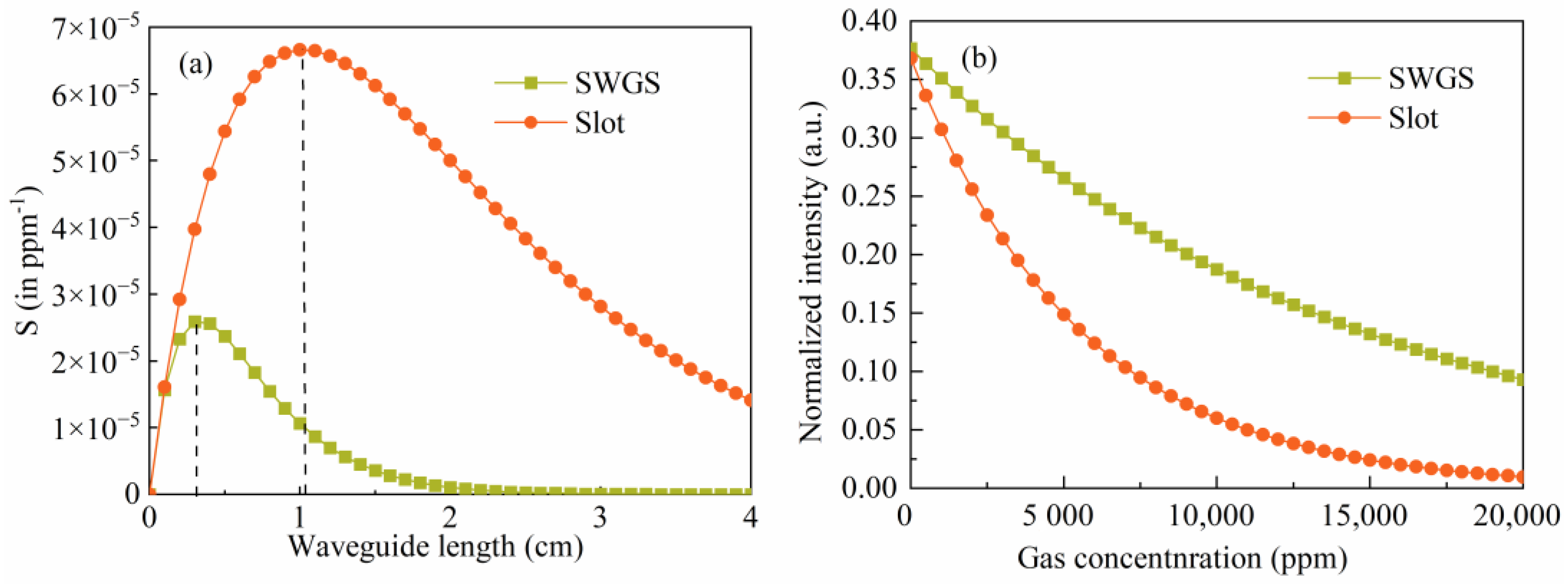
Two optical waveguide sensors based on SOS (silicon-on-sapphire) for detecting CO2 are theoretically proposed. The operational wavelength is 4.23 μm, which is the maximum absorption line of CO2. The power confinement factor (η) value is over 40% and 50%, the propagation loss is 0.98 dB/cm and 2.99 dB/cm, respectively, in the slot waveguide and SWGS (subwavelength grating slot) waveguide. An inverted tapered structure is used for the transition from strip waveguide to slot waveguide and constitutes the sensing absorption region, with the coupling efficiency that can reach more than 90%. When the optimal absorption length of the slot waveguide and SWGS waveguide is 1.02 cm and 0.33 cm, respectively, the maximum sensitivity can reach 6.66 × 10⁻⁵ (ppm−1) and 2.60 × 10⁻⁵ (ppm−1). Furthermore, taking the slot waveguide as an example, spiral and meander structures enable the long-distance sensing path to integrate into a small area.

1. Introduction

The detection of a myriad of gas concentrations for monitoring atmosphere quality [1], observing vital signs [2], and judging security under specified circumstances [3], is of particular significance. At present, the major popular optical gas sensors are NDIR (non-dispersive infrared) sensors based on the spectrum absorption principle, which characterize the gas concentration by detecting the attenuation of optical intensity. The traditional gas sensors frequently apply to air chambers and are disadvantaged due to taking up too much room, high cost, only being used for specified situations, and the difficulty for industrial manufacturing [4,5,6].
For the last few years, semiconductor nanostructures are increasingly full-fledged, which enabled distracted optical components to transform into integrated optical platforms [7]. Most of the refractive index sensors are based on SOI (silicon-on-insulator) structures [8,9,10]. The refractive index change method is inappropriate for monitoring gas concentration in the near-infrared 1.55 µm range. For instance, the specified polymer functional layer was spined on the waveguide surface to enhance the refractive index change for the detected gas [11,12,13]. However, response time, mechanical flexibility, and repeatability are obvious drawbacks for the functional layer sensors. Most absorption footprints of gas are in the mid-infrared region with a high absorption coefficient. Thus, two main orientations are concluded: one is that the plasmonic waveguide with metal-insulator configuration realizes ultra-high sensitivity in the mid-infrared region [14,15], and the other is an integrated gas sensor based on mid-infrared absorption spectroscopy by selecting the absorption wavelength and the compatible semiconductor materials [16,17,18,19]. For the mid-infrared gas absorption sensors, the long sensing path can be concentrated in a small area by different waveguide structures, such as spiral waveguide, meander waveguide, and resonator [7,8,11].
In this paper, the strip waveguide, slot waveguide, SWG (subwavelength grating) waveguide, and SWGS (subwavelength grating slot) waveguide for the mid-infrared carbon dioxide gas sensors are investigated. The values of power the confinement factor are calculated to obtain high sensitivity. Furthermore, a spiral structure and a meander structure are proposed to increase the absorption length directly in a small region. Compared to the traditional mid-infrared gas sensor, the gas sensor designed in this paper achieves high sensitivity and high compactness.

2. Principle and Proposed Structure

There are several absorption windows from the near-infrared region to the mid-infrared region for the carbon dioxide gas. When the concentration of the carbon dioxide is 1ppm under 296 K and 1 atm, the carbon dioxide molecule absorption coefficient is up to 3.778 × 10⁻⁴ (ppm cm)−1 at 4.23 µm [20,21], which is 4–5 orders of magnitude higher than that near the 1.57 µm region. Hence, the 4.23 μm wavelength of the input light is selected.
Most of the sensing chips are composed of silicon material as the core layer, and conventional cladding layer materials including silicon dioxide (SiO2), silicon nitride (Si3N4), and sapphire (Al2O3) [22,23,24]. A high refractive index difference between the core and cladding layer generates a strong evanescent field at the interface of the very small waveguide. Noticeably, silicon dioxide material possesses a significantly large absorption loss above 4.23 µm wavelength [25]. Hence, the sapphire medium, with low absorption at 4.23 µm, is selected as the substrate.
Each gas molecule exhibits one or more absorption peaks, and covers different spectral absorption line intensities at different wavelengths. Figure 1a,b show that the strip waveguide and slot waveguide are surrounded by gas. According to the Lambert-Beer law, the optical power will decrease when transmitting light propagates [26].
I = I 0 e x p   η ε c L α L
I0 represents the initial light intensity, ε is the absorption coefficient at a certain wavelength, c is the concentration of detected gas, and L is marked as the absorption length. α is the loss of waveguide including scattering loss, absorption loss of material and propagation loss of the waveguide, surface contamination loss, etc. η is the power confinement factor, which defines the ratio of evanescent field power in the gaseous region to the total field power. It can be calculated as:
η = P g a s P t o t a l = g a s S z d x d y t o t a l S z d x d y
Pgas and Ptotal are the powers of the coverage area of measured gas and total area, respectively, and Sz is the Poynting vector in the z-axis propagation direction. Therefore, according to the absorption principle, the unknown gas concentration can be measured by detecting the reduction change of the light intensity. From the absorption law, it is realized that the η is the key point, which determines the interaction of the light and gas, and affects the sensitivity. It means η is a trade-off between the sensitivity and the propagation loss.
To obtain the optimized value of η in silicon waveguides, we compare four structures: strip waveguide, SWG waveguide, slot waveguide, and SWGS waveguide, all of which operate at a wavelength of 4.23 µm. A detailed comparison of various characteristics is carried out in Table 1. The height of silicon waveguides is 1.00 µm, for the strip waveguide, and the width of the silicon waveguide is 0.90 µm For the SWG waveguide, the width is 0.90 µm, and the period and duty cycle of subwavelength silicon segments are 1.00 µm and 0.10, respectively. The optical power released by the slot structure is higher than that of the strip structure; this is because the normal component of the electric displacement field is continuous between the silicon waveguide and the air gap, and the electric field is strongly confined in the low-index slot region. The η of the SWG waveguide is also higher than that of the strip waveguide. The SWG structure is composed of periodically arranged subwavelength, silicon segments, and the Bloch mode is excited by light [27,28]. The pattern of the subwavelength grating slot waveguide can be formed by the electron-beam lithography (EBL) and dry-etching, such as inductively-coupled plasma (ICP) etching or reactive-ion etching (RIE). Introducing the SWG structure into the strip waveguide and slot waveguide, respectively, will increase the value of η, and the corresponding propagation loss will increase as shown in Table 1.
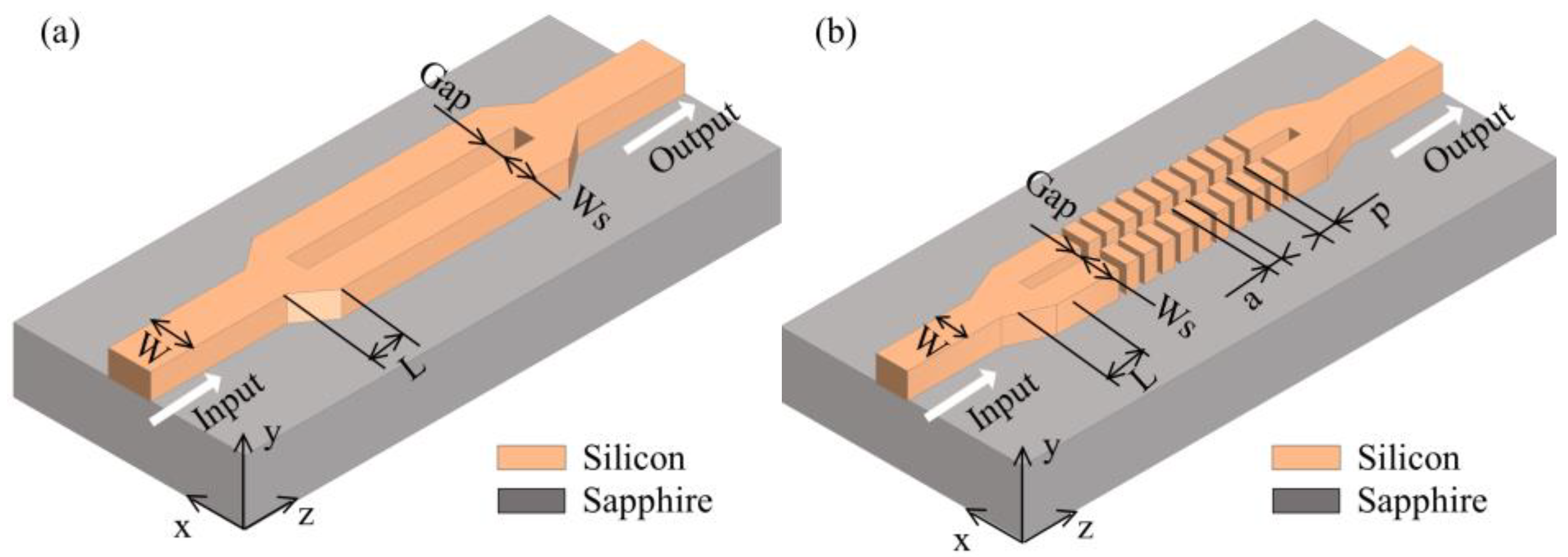
Considering that the light released by the silicon waveguide interacts with the gas to be measured, it is used for gas absorption sensing. Next, the slot waveguide and SWGS waveguide will be simulated for the optimized value of η. Figure 2a,b show relevant parameters such as the width of the strip waveguide (W), the length of the tapered waveguide (L), the width of the slot waveguide (Ws), and the gap size (Gap). For the SWGS waveguide, the period (p) and the segment length (a) of periodic silicon are described in Figure 2b. Up to now, the formation of the majority of slot waveguides originated from mode-coupling between some irregular taper segments [29,30,31], and the width of the slot gap is less than 50 nm. This paper investigates a simple structure, including an inverse taper waveguide between the strip waveguide and slot waveguide, with a gap of 200 nm. The coupling efficiency from the strip waveguide to the slot waveguide can reach 90% when L = 2.00 µm; the coupling efficiency is calculated as the ratio of the optical power at the output of the inverted tapered waveguide, to the optical power at the input of the strip waveguide. The light propagates forward in the gap, generating an absorption phenomenon with the gas to be measured.

3. Simulations and Results

The proposed gas sensor structures consist of the silicon slot waveguides as the core waveguide on the substrate of sapphire for CO2 monitoring, based on the absorption at 4.23 µm. The FDTD (finite-difference time domain) method is used to simulate and analyze the performance of the sensor. Supposing the fundamental TE mode of the light source propagating along the z-axis, TM is not selected as it will cause a higher loss [23]. The height of the silicon waveguide is 1.00 µm. The higher value of η leads to a stronger interaction between CO2 gas and the light. Optimized η is determined by geometrical factors such as W and Ws. In addition, for the SWGS waveguide, the p and a of the periodical silicon segments are 2.00 µm and 0.30 µm, respectively.
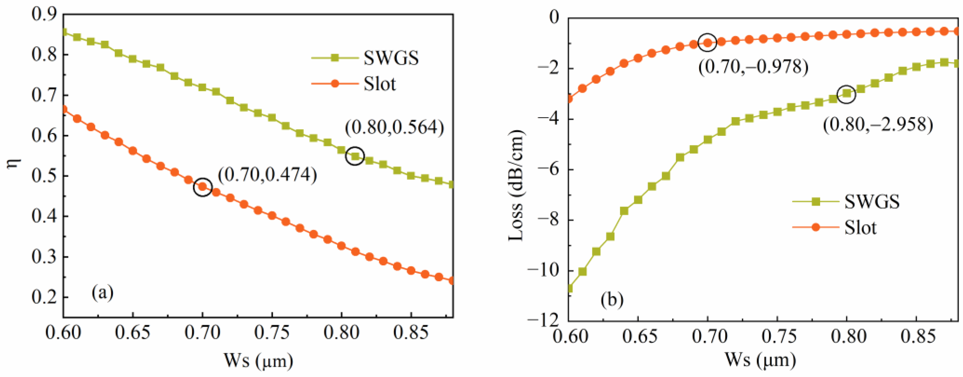
Figure 3a,b, respectively, show that the η and the propagation-loss change with the Ws for the slot waveguide and SWGS waveguide. The pictures show that the optical power released by the SWGS structure is obviously higher than that of the slot structure, but its loss will also increase. When Ws = 0.85 µm, η is 0.56 and 0.33, respectively, in the slot waveguide and SWGS waveguide, which is almost a two-fold difference, and the transmission loss is 2.96 dB/cm and 0.64 dB/cm.
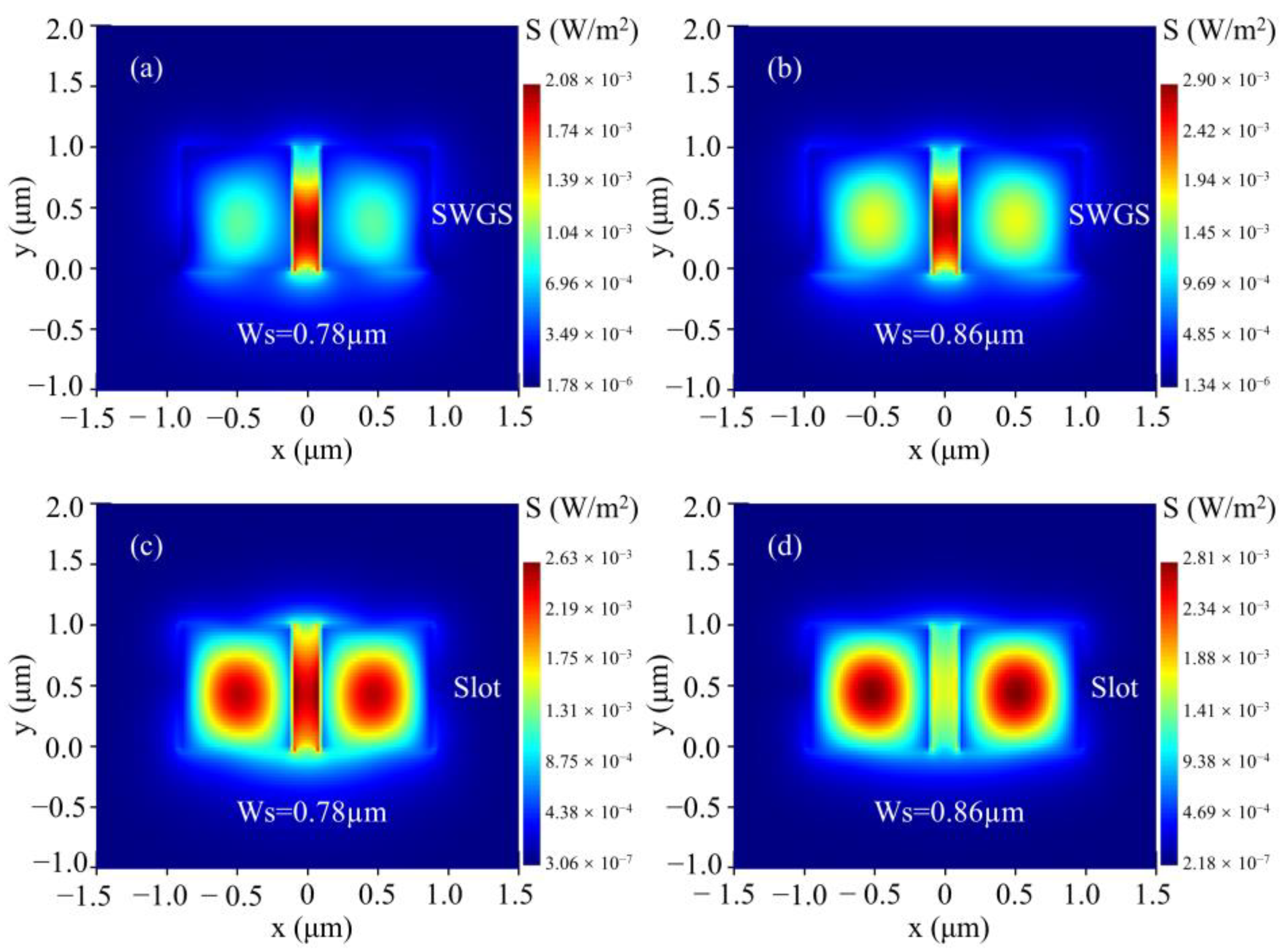
According to the distribution of the Poynting vector on the cross-section of the propagation direction in Figure 4, when the width of the slot waveguide steadily increases, the optical power in the slot region gradually decreases, and most of the light is confined on the bilateral waveguides. When the Ws approaches 0.60 µm, although the η accounts for a relatively high proportion, the propagation loss is much larger and achieves 10.29 dB/cm and 3.20 dB/cm in SWGS and slot waveguide; the TE mode becomes leaky and penetrates the sapphire substrate accordingly. Eventually, for the SWGS waveguide, we choose Ws = 0.80 µm to obtain a relatively low loss, and the Ws of the slot waveguide is 0.70 µm.
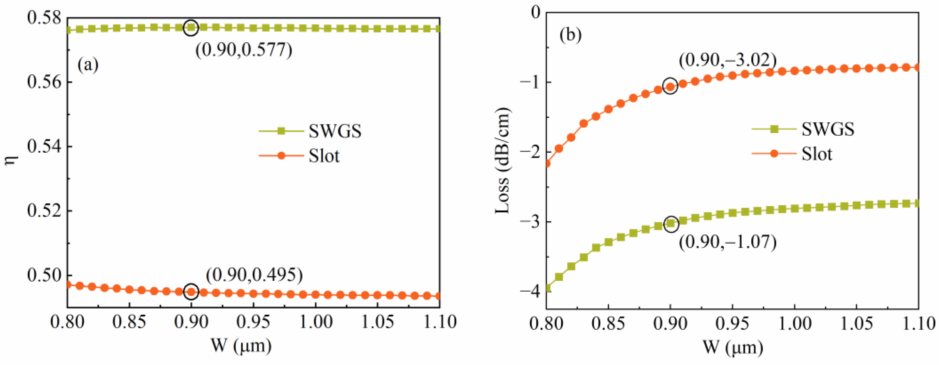
Figure 5a,b show the variation of η and propagation loss as the width of the strip waveguide when the Ws of the SWGS and slot waveguide are 0.80 µm and 0.70 µm, respectively. The factor η is insensitive to the parameters W for the two structures, but W has a relatively large influence on the transmission loss of the waveguide. The larger value of W will confine the light more in the waveguide, providing lower propagation loss; finally, W = 0.90 µm is determined.
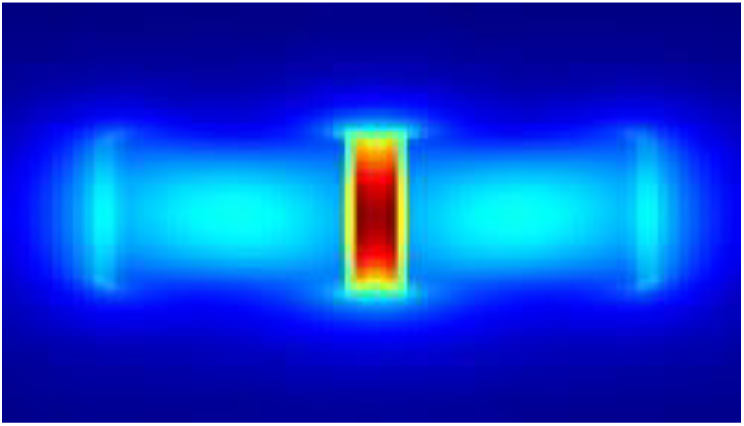
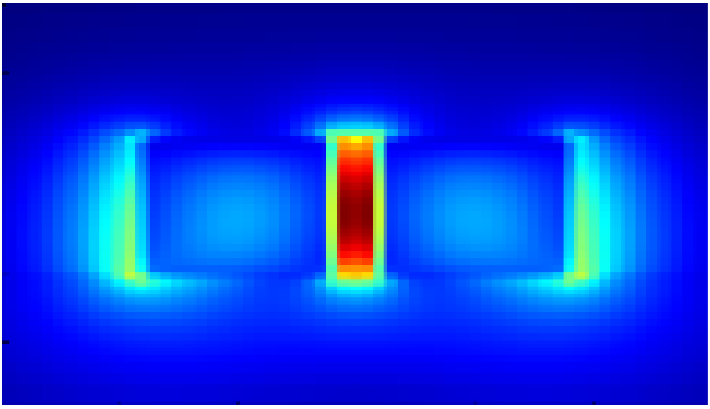
The sensor mainly includes three parts: the conversion from the strip waveguide to the slot waveguide, the transmission of light in the slot waveguide or the SWGS waveguide, and the coupling of light from the slot waveguide to the strip waveguide. Most of the propagating optical field is confined in the slot region of tens of nanometers. The light in the sensing region is contacted by the gas to be measured for absorption. Figure 6a,b display the electric field distribution in the propagating direction with the SWGS and slot structure. The optical power released by the SWGS waveguide is higher than that of the slot waveguide. The SWGS will increase the propagation loss of the SWGS waveguide, so when determining the parameters, the transmission loss of the SWGS waveguide should be minimized.
By simulating and determining the dimensions of the slot waveguide and SWGS waveguide, appropriate parameters can be determined as follows: Gap = 0.20 µm, L = 2.00 µm, W = 0.90 µm, the Ws of the SWGS waveguide is 0.80 µm, and Ws of the slot waveguide is 0.70 µm. S is the sensitivity of the sensor, and is determined by Equation (3)
S = d I / I 0 d c = η ε L e x p η ε c L α L = η ε L I n
A minus sign is indicative of the absorption phenomenon, and In = I/I0 is the normalized intensity of the output light intensity relative to the input light intensity. The sensitivity could be influenced, except for the higher η, the waveguide length and transmission loss, as they are crucial for the sensitivity of the transducer. Differentiating both sides of the Equation (3), S reaches the maximum value at L = 1/(ηεc + α).
When monitoring the CO2 gas, the concentration of gas is assumed for 1 ppm, and the sensitivity as a function of absorption length for the SWGS and slot waveguide, as shown in Figure 7a. Although the SWGS waveguide releases more optical energy to interact with the gas, its sensitivity is lower than slot waveguide, because the transmission loss of the SWGS waveguide is too high. The sensitivity of the SWGS and slot waveguide can reach 2.60 × 10⁻⁵ (ppm−1) and 6.66 × 10⁻⁵ (ppm−1). The waveguide length is called the optimum length when the sensitivity is at its highest, and the optimum lengths of the two structures are 0.33 cm and 1.02 cm, respectively. It is a higher η of the SWGS structure that leads to a shorter optimum length.
Figure 7b shows the variation of normalized intensity versus gas concentration at 4.23 µm with the slot waveguide and the SWGS waveguide; the optimal waveguide lengths are 1.02 cm and 0.33 cm for the two structures. SWGS makes more light release in the slot to interact with the gas, meanwhile, its complex structure brings higher transmission loss, and its sensor sensitivity and light intensity attenuation are lower than the slot structure, so in the mid-infrared region, the slot waveguide is more suitable for gas-absorption sensing than other silicon waveguide structures.
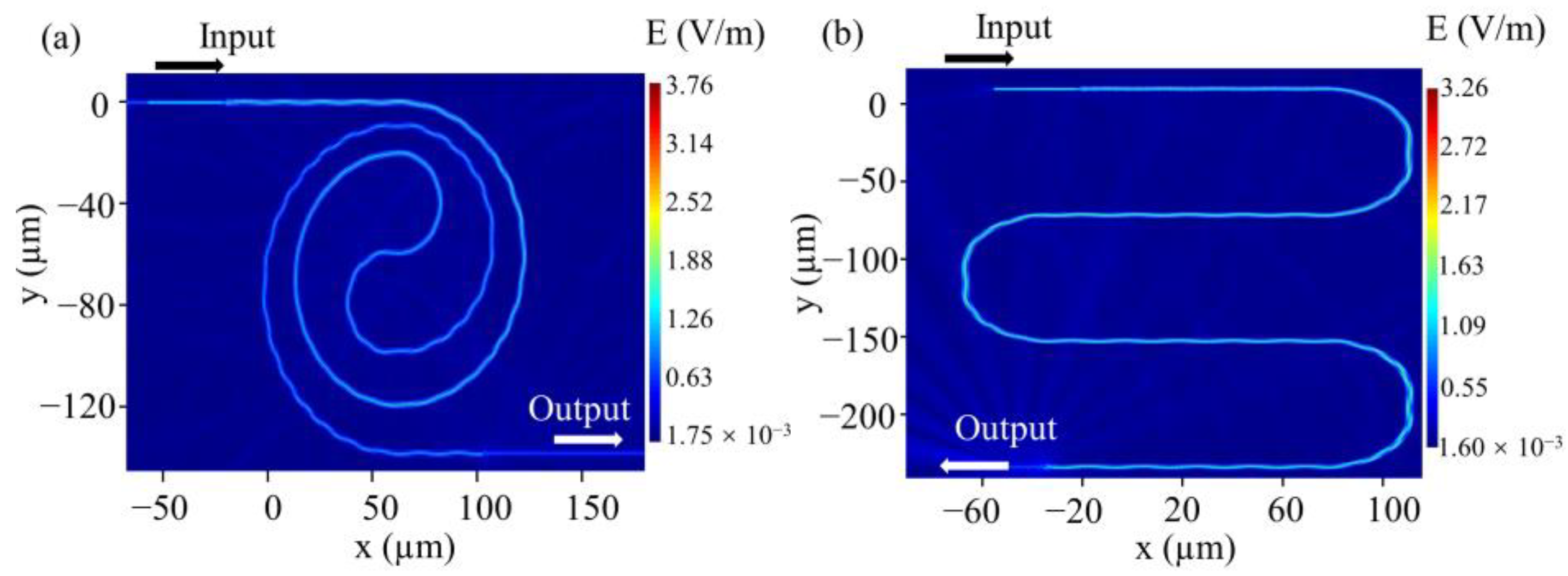
An obvious feature of silicon waveguide used as a gas sensor is that its sensing path can be applied to a small area through different structures, including a spiral structure, meander waveguide, and resonator. Taking the slot waveguide as an example, Figure 8a,b show the transmission electric field distribution of a spiral structure, and meander structure with the slot structure, respectively. Using the spiral or meander structure, the transmission length of several centimeters can be realized in the area of hundreds of microns, which is promising for developing a fully integrated semiconductor chip sensor.

4. Discussion

The performance comparisons including sizes and η with previous research are listed in Table 2. When the operating wavelength is from near-infrared to mid-infrared, the sizes of the waveguide become larger. The η values of slot and SWGS structures in this paper are clearly higher than that of other mid-infrared structures. Meanwhile, compared to literature [17,24], the transmission loss is lower. The higher η value and lower transmission loss will improve the sensitivity of the sensor.

5. Conclusions

In this paper, several silicon waveguides based on the SOS in the mid-infrared region are compared. Considering that the released light is sensitive to changes in the surrounding environment and is used for optical sensing applications, slot waveguides and SWGS waveguides are selected for a more detailed simulation comparison. The power confinement factors of both are 0.47 and 0.56; the optimum lengths are 0.33 cm and 1.02 cm, and the sensitivities can realize 6.66 × 10⁻⁵ (ppm−1) and 2.60 × 10⁻⁵ (ppm−1), respectively, for the slot and SWGS waveguide structures.
For silicon photonic-integrated mid-infrared gas sensors, an obvious feature is that the absorption path can be optimized by different structures, such as spiral waveguide, meander waveguide, or ring resonator. Compared with the traditional mid-infrared carbon dioxide gas sensor, the integrated semiconductor chip sensor can realize long-distance transmission in a small area. Additionally, it is more convenient for the integrated chip sensor to achieve the reference output by silicon waveguide, which is promising for making an industrialized gas sensor on an integrated chip.

Author Contributions

Conceptualization, Y.S. and B.L.; methodology, Y.S. and M.L.; software, Y.S., H.Z., M.L. and J.-J.H.; investigation, Y.S., B.L. and H.Z.; writing—original draft preparation, Y.S. and M.L.; writing—review and editing, Y.S., M.L. and Q.L.; visualization, Y.S., B.L. and M.L.; supervision, M.L., Q.L. and J.-J.H.; project administration, M.L. and J.-J.H. All authors have read and agreed to the published version of the manuscript.

Funding

This research was funded by the National Natural Science Foundation of China grant number [No.62027825], the National Key R&D Program of China grant number [No.2020YFC2004600], the 111 Project of China grant number [No.D21009], Natural Science Foundation of Jilin Province grant number [No.20220101130JC], and Shandong Provincial Natural Science Foundation grant number [ZR2019MC069].

Institutional Review Board Statement

Not applicable.

Informed Consent Statement

Not applicable.

Data Availability Statement

The authors confirm that the data supporting the findings of this study are available within the article.

Acknowledgments

The authors would like to thank Shiya Zhang and Tuo Chen for their discussions on theory and simulation.

Conflicts of Interest

The authors declare no conflict of interest.

References

  1. Gibson, D.; MacGregor, C. A Novel Solid State Non-Dispersive Infrared CO2 Gas Sensor Compatible with Wireless and Portable Deployment. Sensors 2013, 13, 7079–7103. [Google Scholar] [CrossRef] [Green Version]
  2. Li, X.; Zhuang, Z.; Qi, D.; Zhao, C. High sensitive and fast response humidity sensor based on polymer composite nanofibers for breath monitoring and non-contact sensing. Sens. Actuators B Chem. 2020, 330, 129239. [Google Scholar] [CrossRef]
  3. Liu, Z.; Zheng, C.; Chen, C.; Li, Y.; Xie, H.; Ren, Q.; Wang, Y.; Tittel, F.K. ICL-based mid-infrared carbon dioxide sensor system for deep-sea natural gas hydrate exploration. Opt. Express 2019, 27, 5598–5609. [Google Scholar] [CrossRef] [PubMed]
  4. Pandey, S.K.; Kim, K.H. The Relative Performance of NDIR-based Sensors in the Near Real-time Analysis of CO2 in Air. Sensors 2007, 7, 1683–1696. [Google Scholar] [CrossRef] [PubMed] [Green Version]
  5. Vincent, T.A.; Gardner, J.W. A low cost MEMS based NDIR system for the monitoring of carbon dioxide in breath analysis at ppm levels. Sens. Actuators B Chem. 2016, 236, 954–964. [Google Scholar] [CrossRef] [Green Version]
  6. Weigel, C.; Grewe, A.; Sinzinger, S.; Hoffmann, M. A microoptical sidestream cuvette based on fast passive gas exchange for capnography. Sens. Actuators A Phys. 2018, 276, 68–75. [Google Scholar] [CrossRef]
  7. Yazici, M.S.; Dong, B.; Hasan, D.; Sun, F.; Lee, C. Integration of broadband MEMS IR detector with MIR waveguides for sensing applications. Opt. Express 2020, 28, 11524–11537. [Google Scholar] [CrossRef] [PubMed]
  8. Zhang, Y.; Zou, J.; Cao, Z.; He, J.J. Temperature-insensitive waveguide sensor using a ring cascaded with a Mach-Zehnder interferometer. Opt. Lett. 2019, 44, 299–302. [Google Scholar] [CrossRef]
  9. Xie, Z.; Cao, Z.; Liu, Y.; Zhang, Q.; Zou, J.; Shao, L.; Wang, Y.; He, J.; Li, M. Highly-sensitive optical biosensor based on equal FSR cascaded microring resonator with intensity interrogation for detection of progesterone molecules. Opt. Express 2017, 25, 33193–33201. [Google Scholar] [CrossRef]
  10. Prasad, P.R.; Selvaraja, S.K.; Varma, M.M. High precision measurement of intensity peak shifts in tunable cascaded microring intensity sensors. Opt. Lett. 2016, 41, 3153–3156. [Google Scholar] [CrossRef] [PubMed]
  11. Mi, G.; Horvath, C.; Aktary, M.; Van, V. Silicon microring refractometric sensor for atmospheric CO2 gas monitoring. Opt. Express 2016, 24, 1773–1780. [Google Scholar] [CrossRef] [PubMed]
  12. Mi, G.; Horvanth, C.; Van, V. Silicon photonic dual-gas sensor for H2 and CO2 detection. Opt. Express 2017, 25, 16250–16259. [Google Scholar] [CrossRef] [PubMed]
  13. Li, H.; Sun, B.; Yuan, Y.; Yang, J. Guanidine derivative polymer coated microbubble resonator for high sensitivity detection of CO2 gas concentration. Opt. Express 2019, 27, 1991–2000. [Google Scholar] [CrossRef] [PubMed]
  14. El Shamy, R.S.; Khalil, D.; Swillam, M.A. Mid infrared optical gas sensor using plasmonic Mach-Zehnder interferometer. Sci. Rep. 2020, 10, 1239. [Google Scholar] [CrossRef] [Green Version]
  15. Saeidi, P.; Jakoby, B.; Pühringer, G.; Tortschanoff, A.; Stocker, G.; Dubois, F.; Spettel, J.; Grille, T.; Jannesari, R. Designing mid-infrared gold-based plasmonic slot waveguides for CO2 sensing applications. Multidiscip. Digit. Publ. Inst. 2021, 21, 2269. [Google Scholar] [CrossRef] [PubMed]
  16. Chandar, V.; Ranjan, R. Performance analysis of different slot waveguide structures for evanescent field based gas sensor applications. Opt. Quantum Electron. 2021, 53, 457–472. [Google Scholar] [CrossRef]
  17. Kumari, B.; Barh, A.; Varshney, R.; Pal, B. Silicon-on-nitride slot waveguide: A promising platform as mid-IR trace gas sensor. Sens. Actuators B Chem. 2016, 236, 759–764. [Google Scholar] [CrossRef]
  18. Butt, M.A.; Khonina, S.N.; Kazanskiy, N.L. Silicon on silicon dioxide slot waveguide evanescent field gas absorption sensor. J. Mod. Opt. 2018, 65, 174–178. [Google Scholar] [CrossRef]
  19. Butt, M.A.; Degtyarev, S.A.; Khonina, S.N.; Kazanskiy, N.L. An evanescent field absorption gas sensor at mid-IR 3.39μm wavelength. J. Mod. Opt. 2017, 64, 1892–1897. [Google Scholar] [CrossRef] [Green Version]
  20. Rothman, L.S.; Jacquemart, D.; Barbe, A.; Benner, D.C.; Birk, M.; Brown, L.R.; Carleer, M.R.; Chackerian, C., Jr.; Chance, K.; Coudert, L.E.A. The HITRAN 2004 molecular spectroscopic database. J. Quant. Spectrosc. Radiat. Transf. 2005, 96, 139–204. [Google Scholar] [CrossRef] [Green Version]
  21. Hill, C.; Gordon, I.E.; Kochanov, R.V.; Barrett, L.; Wilzewski, J.S.; Rothman, L.S. HITRAN online: An online interface and the flexible representation of spectroscopic data in the HITRAN database. J. Quant. Spectrosc. Radiat. Transf. 2016, 177, 4–14. [Google Scholar] [CrossRef] [Green Version]
  22. Koompai, N.; Chaisakul, P.; Limsuwan, P.; Le Roux, X.; Vivien, L.; Marris-Morini, D. Design and simulation investigation of Si3N4 photonics circuits for wideband on-chip optical gas sensing around 2µm optical wavelength. Sensors 2021, 21, 2513. [Google Scholar] [CrossRef] [PubMed]
  23. Ranacher, C.; Tortschanoff, A.; Consani, C.; Moridi, M.; Grille, T.; Jakoby, B. Photonic Gas Sensor Using a Silicon Strip Waveguide. Multidiscip. Digit. Publ. Inst. Proc. 2017, 1, 547. [Google Scholar]
  24. Huang, Y.; Kalyoncu, S.K.; Zhao, Q.; Torun, R.; Boyraz, O. Silicon-on-sapphire waveguides design for mid-IR evanescent field absorption gas sensors. Opt. Commun. 2014, 313, 186–194. [Google Scholar] [CrossRef]
  25. Soref, R.A.; Emelett, S.J.; Buchwald, W.R. Silicon waveguided components for the long-wave infrared region. J. Opt. A Pure Appl. Opt. 2006, 8, 840–848. [Google Scholar] [CrossRef] [Green Version]
  26. Sibert, R.; Muller, J. Infrared integrated optical evanescent field sensor for gas analysis Part I: System design. Sens. Actuators A Phys. 2005, 119, 138–149. [Google Scholar] [CrossRef]
  27. Ruan, Z.; Zhou, N.; Zheng, S.; Cao, X.; Long, Y.; Chen, L.; Wang, J. Releasing the light field in subwavelength grating slot microring resonators for athermal and sensing applications. Nanoscale 2020, 12, 15620–15630. [Google Scholar] [CrossRef]
  28. Bock, P.J.; Cheben, P.; Schmid, J.H.; Lapointe, J.; Delâge, A.; Janz, S.; Aers, G.C.; Xu, D.-X.; Densmore, A.; Hall, T.J. Subwavelength grating periodic structures in silicon-on-insulator: A new type of microphotonic waveguide. Opt. Express 2010, 18, 20251–20262. [Google Scholar] [CrossRef] [Green Version]
  29. Zou, Y.; Subbaraman, H.; Chakravarty, S.; Xu, X.; Hosseini, A.; Lai, W.-C.; Wray, P.; Chen, R.T. Grating coupled silicon-on-sapphire integrated slot waveguides operating at mid-infrared wavelengths. Opt. Lett. 2014, 39, 3070–3073. [Google Scholar] [CrossRef] [Green Version]
  30. Feng, N.N.; Sun, R.; Kimerling, L.C.; Michel, J. Lossless strip-to-slot waveguide transformer. Opt. Lett. 2007, 32, 1250–1252. [Google Scholar] [CrossRef]
  31. Butt, M.A.; Khonina, S.N.; Kazanskiy, N.L. Ultrashort inverted tapered silicon ridge-to-slot waveguide coupler at 1.55µm and 3.392µm wavelength. Appl. Opt. 2020, 59, 7821–7828. [Google Scholar] [CrossRef] [PubMed]
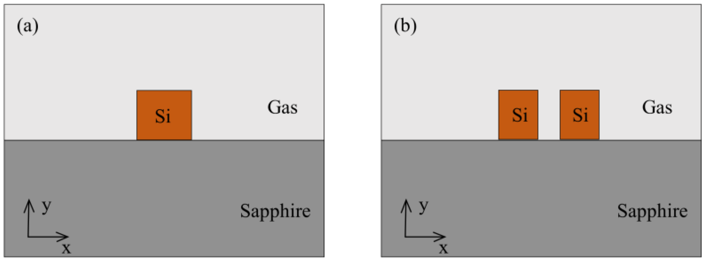
Figure 1. A cross-section schematic diagram of the proposed SOS-based structure (a) strip waveguide; (b) slot waveguide.
Photonics 10 00120 g001
Figure 2. The structure diagram of the proposed sensor (a) slot waveguide; (b) SWGS waveguide.
Photonics 10 00120 g002
Figure 3. (a) Variation of η versus Ws; (b) variation of propagation loss versus Ws for the SWGS and slot waveguide.
Photonics 10 00120 g003
Figure 4. The distribution of the Poynting vector on the cross-section for SWGS waveguide when Ws is (a) 0.78 µm; (b) 0.86 µm; for slot waveguide when Ws is (c) 0.78 µm; (d) 0.86 µm.
Photonics 10 00120 g004
Figure 5. (a) Variation of η versus W; (b) variation of propagation loss versus W for the SWGS and slot waveguide.
Photonics 10 00120 g005
Figure 6. The electric field distribution in the propagating direction: (a) slot waveguide; (b) SWGS waveguide.
Photonics 10 00120 g006
Figure 7. (a) Variation of sensitivity with waveguide length; (b) variation of normalized intensity with dioxide carbon gas concentration for the SWGS waveguide and slot waveguide.
Photonics 10 00120 g007
Figure 8. The electric field distribution with different structures: (a) spiral structure of slot waveguide; (b) meander structure of slot waveguide.
Photonics 10 00120 g008
Table 1. Electric field distribution, calculated η and propagation loss for strip waveguide, SWG waveguide, slot waveguide, and SWGS waveguide.
Waveguide TypeStripSWGSlotSWGS
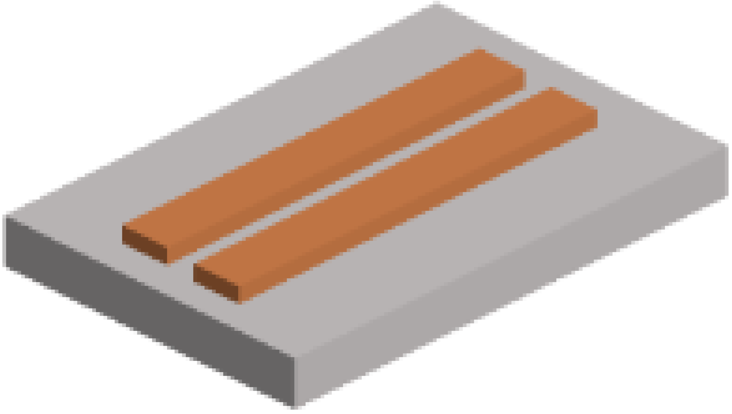
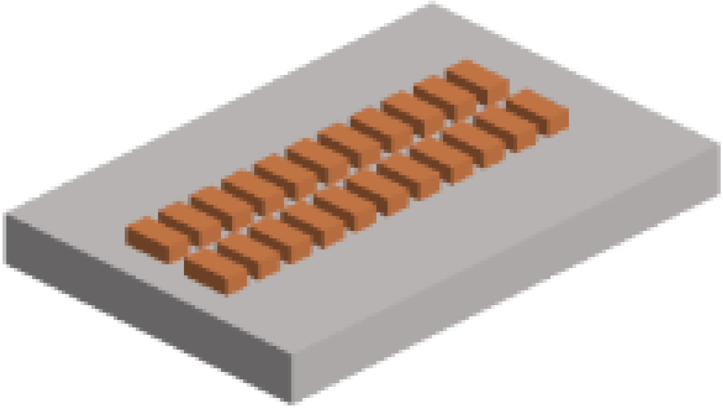
StructurePhotonics 10 00120 i001Photonics 10 00120 i002Photonics 10 00120 i003Photonics 10 00120 i004
Mode profilePhotonics 10 00120 i005Photonics 10 00120 i006Photonics 10 00120 i007Photonics 10 00120 i008
η0.150.380.470.56
Loss (dB/cm)0.0231.540.982.96
Table 2. Comparisons of various parameters under different waveguide structures.
Waveguide TypeWavelength (μm)Parameters Sizes (μm)η
SWGS [27]1.55H = 0.34; Ws = 0.30; Gap = 0.10; p = 0.20; a = 0.100.69
Slot [17]3.00H = 1.70; Ws = 0.43; Gap = 0.100.43
Slot [24]4.23H = 0.60; W = 1.000.14
Slot [24]4.23H = 0.60; Ws = 1.60; Gap = 0.200.27
Slot (our research work)4.23H = 1.00; Ws = 0.70; Gap = 0.200.47
SWGS (our research work)4.23H = 1.00; Ws = 0.80; Gap = 0.20; p = 2.00; a = 0.300.56
Disclaimer/Publisher’s Note: The statements, opinions and data contained in all publications are solely those of the individual author(s) and contributor(s) and not of MDPI and/or the editor(s). MDPI and/or the editor(s) disclaim responsibility for any injury to people or property resulting from any ideas, methods, instructions or products referred to in the content.