Communication

A Theoretical Sub-0.1 dB Loss Single Mode Fiber-To-Chip Edge Coupler for Silicon Nitride Waveguides

National Engineering Research Center of Electromagnetic Radiation Control Materials, University of Electronic Science and Technology of China, Chengdu 610054, China
*
Authors to whom correspondence should be addressed.
Photonics 2023, 10(3), 231; https://doi.org/10.3390/photonics10030231
Submission received: 23 January 2023 / Revised: 13 February 2023 / Accepted: 14 February 2023 / Published: 21 February 2023
(This article belongs to the Section Optoelectronics and Optical Materials)

Abstract

:
A low loss optical interconnection between optical fibers and photonic integrated circuits is critical for high performance photonic systems. In the past decade, spot size converters, subwavelength waveguide grating (SWG) structures, and different refractive index materials have been applied to allow efficient coupling between the fiber and the photonic chips. However, it is still challenging to achieve low-loss coupling when interfacing high index contrast waveguides such as SiN with SMF-28 fibers. In this work, we report a multilayer edge-coupler using SiOxN materials with different indices to allow for efficient edge coupling between SMF-28 fiber and SiN single mode waveguides. A coupling loss of 0.068 dB for the TM mode was achieved theoretically at a 1550 nm wavelength, with a 1 dB alignment tolerance offset of 2.4 μm.

1. Introduction

Silicon photonic integrated circuits (SiPs) have attracted great research interest for optical and data communication applications. Thanks to the high index contract of Si and SiN to SiO2, silicon photonic devices enjoys advantages of small footprint, low cost, and large-scale integration capability using complementary metal oxide semiconductor (CMOS) processes [1,2,3]. However, a key challenge for silicon photonic chips is the large mode mismatch between the high index contrast waveguides to low index contrast fibers, preventing efficient coupling of light in and out of SiPs. The typical mode size of several hundred nanometers in Si and SiN waveguides couples poorly to the 10.4 μm diameter mode in single mode fibers (SMF-28). Up to 3 dB coupling loss was observed in butt-coupling structures, causing a major contribution to the insertion loss. As a comparison, planar lightwave circuits (PLCs) based on low index contrast silica waveguides can show less than 0.1 dB coupling loss to SMF-28 [4]. Therefore, coupling efficiency is considered one of the major roadblocks for the application of SiPs [5].
To solve the problems above, great efforts have been devoted in the past two decades to improving the coupling structures [6,7,8]. Fiber-to-chip couplers can be categorized as grating couplers and edge couplers. The latter are particularly attractive due to their low coupling loss and wide coupling bandwidth. In past years, the main theme to improve the edge coupler was to control the waveguide modal profile to match that of the SMF-28. The first proposal was the inverse taper structure [9,10,11,12]. This structure operated by compressing the size of the waveguide core at the end facet. The effective refractive index of the waveguide mode could be reduced, and the mode profile was expanded. A typical coupling loss of 1 dB was observed between the Si waveguide to the lensed fibers using single inverse taper structures [10]. However, for SMF-28, the waveguide mode size was not large enough for efficient coupling. To solve this problem, researchers proposed multiple inverse taper structures to further enlarge the mode size. A trident structure (multiple inverse taper structures in the horizontal direction) [13,14] was proposed to show less than 1 dB coupling loss with SMF-28. Recently, He et al. proposed one of the best multiple inverse taper coupling structures [15]. Theoretical and experimental coupling losses of 0.76 dB and 2.22 dB, respectively, were achieved for the TE mode at a 1550 nm wavelength. To achieve effective mode overlap in the out-of-plane direction, a multi-layer structure (multiple inverse taper structures in the vertical direction) was proposed [16]. By introducing multiple SiN layers, the mode size could be better matched with the SMF-28. Sun S et al. proposed a multi-layer structure composed of five SiN inverse tapers [17]. It finally achieved a 0.44 dB coupling loss for the TM mode at a wavelength of 1550 nm. Ravi S. Tummidi et al. proposed a similar SiN coupling structure and experimentally demonstrated a coupling loss of 0.5 dB at a wavelength of 1310 nm for the TE mode [18]. Xuyue Lang et al. proposed a multilayer silicon nitride-assisted inverted cone waveguide edge coupler [19]. The coupling loss of the structure was 0.33 dB. In order to further control the effective refractive index of the waveguide mode, SWG structures were introduced in edge coupler designs [20,21,22]. P. Cheben et al. applied SWG to a single inverse taper structure [20], achieving 1.19 dB coupling loss for the TE mode between the SiN waveguide and the SMF-28. Martin Papes et al. proposed a multi-layer coupling structure based on SWG [23]. A coupling efficiency over 90% was achieved in simulation for the TE mode. Moreover, materials with different refractive indices, such as SiOxN, were used to control the mode profile [24,25]. By introducing SiOxN as the cladding layer of SiN inverse tapers, 0.38 dB and 0.85 dB coupling losses between SiN waveguides to SMF-28 were theoretically and experimentally, respectively, demonstrated recently [26]. Despite significant progress, the coupling loss of SiN waveguides to SMF-28 is still several times higher than that of PLCs (<0.1 dB). Therefore, it is very important to develop new coupling structures with higher coupling efficiency.
In this work, we theoretically proposed a SiN edge coupler to SMF-28 with sub-0.1 dB coupling loss. We noticed that although the mode size mismatch has been improved in previous studies, the field distribution still shows a relatively large mismatch between the waveguide and the fiber. We explored an index profile design by introducing SiOxN layers and SiN waveguides with different indices at the coupling facet, which led to highly matched field distributions with the fiber mode. Considering the critical dimension of 180 nm in the standard SiN photonics manufacturing process, the proposed device showed 98.45%/95% mode overlap efficiency and less than 0.1 dB/0.4 dB coupling loss for the TM/TE modes at a 1550 nm wavelength, respectively.

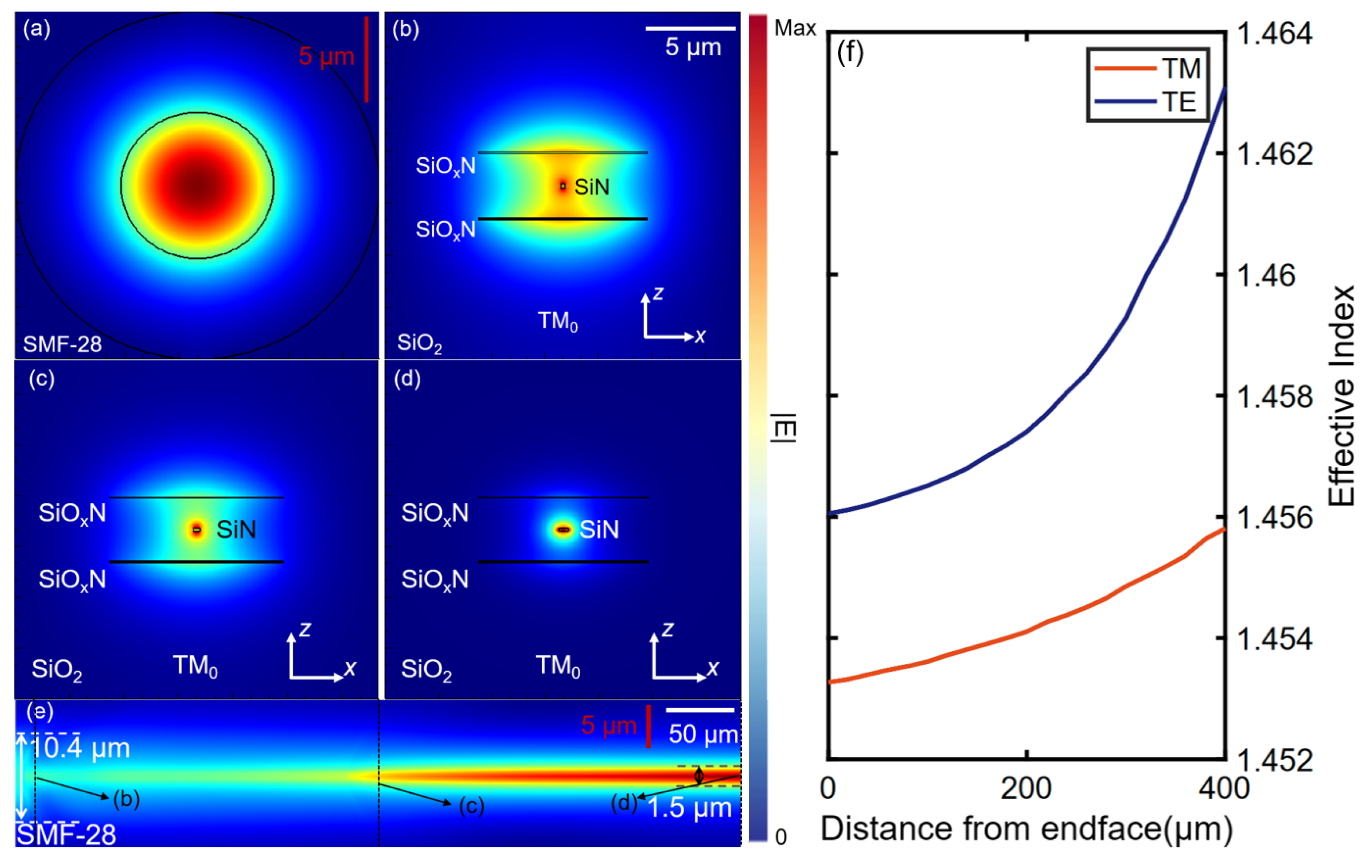
2. Device Structure and Operation Mechanism

The modal overlap efficiency   η 1   of the fiber and the waveguide facet can be expressed as follows [27]:
η 1 = E 1 × E 2 d A 2 E 1 2 d A × E 2 2 d A
where E1 and E2 represent the electric field of the fiber mode and the complex electric field amplitude of the edge coupler end facet, respectively. A is the mode field distribution area at the fiber end face and the edge coupling end face. The maximum coupling efficiency is achieved by matching the electric field distribution of the mode at the end facet as consistently as possible with that of the fiber. After the interface coupling, the mode should be gradually converted to a standard SiN waveguide using a spot size converter (SSC). We define η2 as the mode conversion efficiency of the edge coupler. The total coupling efficiency η is multiplied by η1 and η2. A linear taper structure is used in this study to allow adiabatic mode evolution.
Figure 1 shows the designed edge coupler structure. The structure consists of two parts. The first part is an end-face coupling structure that matches with the single fiber mode profile. The second part is an adiabatic tapering structure with a length of L, which transforms the mode to standard 400 nm thick, 1 mm wide SiN waveguides. The end-face coupling structure consists of three-layers. The middle layer is a SiN waveguide. The upper and lower layers are symmetrically placed SiOxN slabs with n = 1.75. The claddings are SiO2. Figure 1b shows the front view of the end-coupling structure. Figure 1c shows the coupler geometry of the end facet. The mode profile distribution is mainly determined by the following six parameters: the width w1 and height h2 of the central waveguide, the thickness h3 and width w5 and refractive index of the upper and lower SiOxN layers, and the space between the upper and lower SiOxN layers (h4). Figure 1d shows the geometry of the SSC. Figure 1e shows a sketch of the Ez field distribution at the end facet for the fundamental TM mode along the z-axis compared to the TM0 mode of the SMF fiber. Calculated using Equation (1), the mode field overlap efficiency is 99%. For the adiabatic tapering structure, the thickness of the SiN waveguide in the intermediate layer remains constant. The width of the waveguide gradually widens to w6 within the length of L1. The effective index of the waveguide mode increases. When the effective index surpasses the index of SiOxN, the mode gradually tapers from the top and bottom SiOxN layers to the center SiN waveguide. In this way, tapering structures are no longer needed in the top and bottom SiOxN layers, and the fabrication can be greatly simplified. It should be noted that although SiOxN layers can be easily fabricated using chemical vapor deposition tools [17], when only SiN material is available, SWG structures can also be used to modulate the effective index of SiN to mimic the SiOxN layers.
Figure 2 shows the mode profiles in the SMF-28 at the end facet and along the SSC simulated using Lumerical. The optimized device geometries are w1 = h2 = 210 nm, h3 = 65 nm, h4 = 3.8 μm, and w5 = 9.5 μm. The SSC structure has w6 = 500 nm and L1 = 400 μm. The refractive index of SiOxN is n = 1.7, corresponding to the chemistry of Si3O1.6N2.4 [28]. From Figure 2b we can see that the mode at the end facet is almost circularly distributed. For this end-face structure, no higher-order modes are excited. The electric field intensity gradually decreases from the center to the edge, mimicking the field distribution of the fiber mode. As the mode propagates down the SSC, the field gradually localizes in the center SiN waveguide. When the center waveguide width increases to 500 nm, the waveguide mode is completely confined in the SiN waveguide, as shown in Figure 2d. In this process, the effective refractive index is gradually changed. Figure 2e shows the mode profile along the SSC. We can see that the mode width is adiabatically tapered from 10.4 μm to 1.5 μm. Figure 2f shows the relationship between the effective index and the distance from the end face in TE and TM modes.
If the thickness of the central SiN waveguide is different from the thickness of the transmission waveguide (210 nm), an additional tapering structure (L2 and L3) can be used. For instance, when coupling to a 400 nm SiN waveguide, the SiN waveguide width is further tapered from 500 nm (w6) to 1.8 μm (w4) over a length of L2 = 500 μm. An inverse tapered SiN structure can be fabricated on top of the 1.8 mm-wide SiN waveguide. The tip width of the SiN inverse taper is set as 200 nm considering the fabrication critical dimension. The mode is then tapered down to the 400 nm SiN waveguide within the length of 500 μm (L3). The ridge waveguide gradually tapers into a channel waveguide. The final waveguide width is 1 μm.

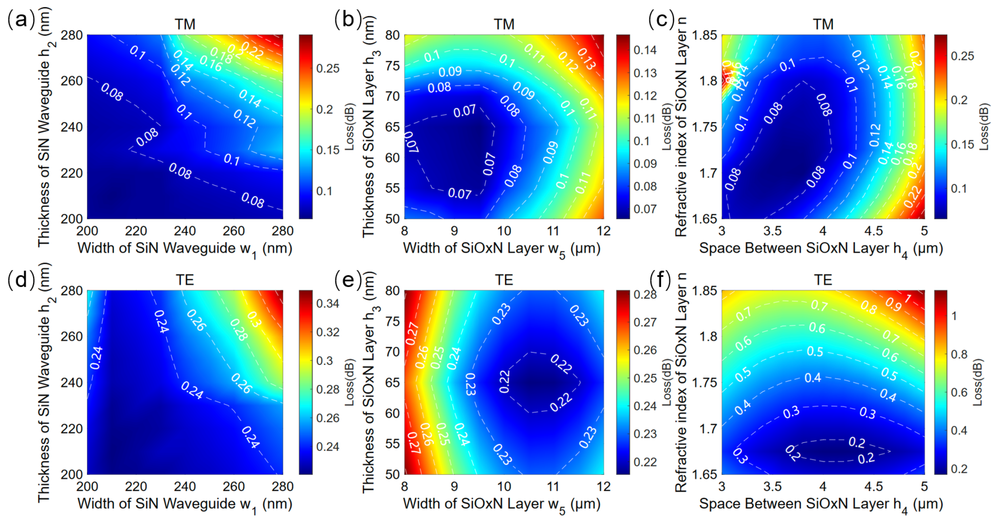
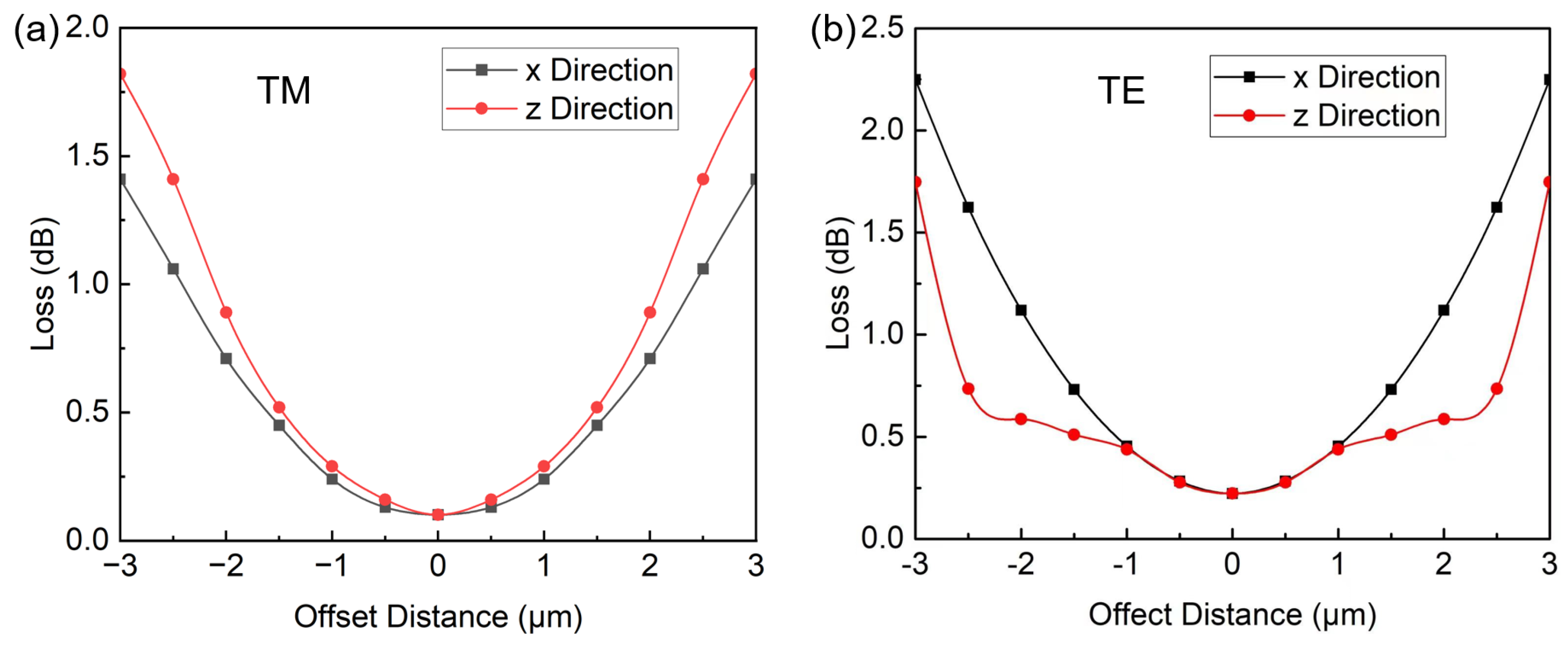
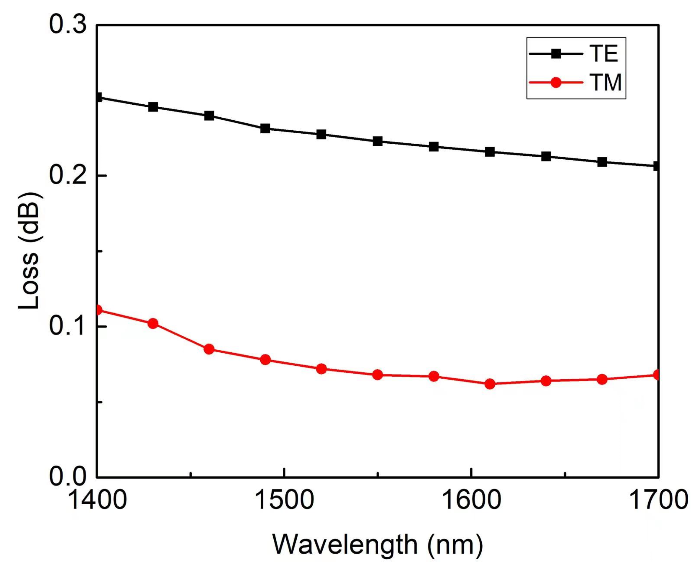
3. Device Performance

We then simulated the coupling loss at a 1550 nm wavelength for the edge coupler. For TM mode, the coupling loss from the end face to the fiber was only 0.068 dB. The loss was all caused by the mismatch of the mode profile, with almost 64 dB reflection loss. The loss caused by the SSC from the end facet to a 210 nm wide SiN waveguide was 0.03 dB. Increasing the length of this part could further reduce the loss. Therefore, the total coupling loss for TM mode was less than 0.1 dB at 1550 nm. For TE mode, the mode overlap efficiency was 0.22 dB, and the SSC-induced loss was 0.08 dB. The total coupling loss for TE mode was 0.3 dB. When considering tapering to a 400 nm SiN waveguide, the total coupling loss of the coupling structure for TM mode increased to 0.37 dB. The loss for TE mode was also less than 0.9 dB. The increased coupling loss was mainly attributed to the scattering at the SiN ridge waveguide junction, which could be mitigated by using processes with smaller critical dimensions or SWG structures.
Figure 3 shows the influence of each parameter on the overall coupling efficiency for TM mode and TE mode. The parameters w1 and h2 regulate the distribution of the mode field near the central SiN waveguide; w5 and h3 regulate the distribution of the mode field near the upper and lower waveguides; and h4 and n regulate the overall mode field distribution. Based on the results, the structure showed a large fabrication tolerance. The excess loss did not exceed 0.1 dB when a single device parameter changed by 10 percent. The optimal structural dimension parameters were w1 = h2 = 210 nm, h3 = 65 nm, h4 = 3.8 μm, and w5 = 9.5 μm. The structure had a minimum size of 200 nm, which fully met the process preparation requirements.
The proposed coupler showed a large alignment tolerance. Figure 4 shows the effect of alignment error on coupling loss. For the TM mode, the 1 dB offset tolerance distance was approximately 2.4 μm in the x-direction and 2.1 μm in the z-direction. For the TE mode, the 1 dB offset tolerance distance was approximately 1.8 μm in the x-direction and 2.7 μm in the z-direction. The offset tolerance of PLCs in the x-direction and z-directions was 2.2 μm, which was almost identical to this structure. The x-direction tolerance in TM mode and the z-direction tolerance in TE mode were even better than those of PLCs [4].
Figure 5 shows the influence of wavelength on coupling efficiency for TM mode and TE mode, respectively. For TM mode or TE mode, the variation of the coupling loss did not exceed 0.1 dB when the wavelength was varied from 1400 nm to 1700 nm. The coupling loss decreased with increases in the wavelength. Since this structure is optimal for TM mode at 1550 nm, the mode field for the TE mode was slightly smaller than that of SMF-28. Thus, as the wavelength increased, the mode field of the TE mode increased, and the loss decreased. For the TM mode, the loss was almost constant. For the TM mode, sub-0.1 dB coupling loss was observed from 1400 nm to 1700 nm, covering the entire S to U bands. Therefore, this structure exhibited a high operation bandwidth with low coupling loss. The structure also had a PDL (polarization-dependent loss) of only 0.14 dB, comparable to the best value reported so far [17].
Figure 6 presents the loss of edge couplers with SMF-28 fibers in the literature [29,30,31,32,33,34]. Although our proposed device was relatively longer, it showed the advantage of lower coupling loss compared to other structures. The overall length of the device mainly depends on the dimensions of the transmission waveguide. The device lengths for different transmission waveguide sizes can be different. Therefore, we focused on the coupling loss of the end-face coupler. Moreover, the device structure was fully compatible with state-of-the-art SiN waveguide platforms. For TM mode, the sub-0.1 dB coupling loss and large fabrication tolerance were even comparable to PLC devices, making our device highly attractive in ultracompact silicon photonic chips for both optical communication and data communication applications.

4. Discussion

The preparation process of this structure is relatively complicated, but the minimum preparation process of this structure is 200 nm, and it meets the minimum fabrication line width of lithography 193. It can be produced in the future. On the SiO2 substrate, we first used sputtering/plasma-enhanced chemical vapor deposition (PECVD)/low pressure chemical vapor deposition (LPCVD) to prepare a layer of 65 nm SiOxN. We performed photolithography and etching on the SiOxN layer to obtain the desired pattern. PECVD can be continually used for SiO2 growth, and then sputtering/PECVD/LPCVD can be used to deposit a 400 nm SiN film, which is etched twice to make it into the shape of the central waveguide. The fabrication method of the upper layer SiOxN is the same as that of the lower layer.

5. Conclusions

In this work, we report low loss edge coupling structures between SiN waveguides and SMF-28. By introducing SiOxN layers with different indices at the edge facet, the waveguide mode field shows 98.45% overlapping efficiency with the SMF-28 mode, allowing sub-0.1 dB coupling loss between the waveguide and the fiber. There are two reasons why this structure can achieve low coupling loss. One reason is that we increased the overlap of the electric field distribution between the coupling modes of the spot size converter and the SMF-28 fiber by changing the size of the central SiN waveguide; another one is that we improved the degree of matching between the coupling modes of the spot size converter and the SMF-28 fiber by adjusting the size, refractive index, and spacing of the SiOxN layer. The coupling loss and the total loss for the entire device reached as low as 0.068 dB and 0.098 dB, respectively, for the TM mode at a 1550 nm wavelength. The proposed structure also features the advantages of large fabrication tolerance, large alignment tolerance, wide operation bandwidth, and low polarization-dependent loss. Our work provides a promising edge coupling structure for silicon photonic integrated circuits.

Author Contributions

Conceptualization, D.W. and W.Y.; methodology, L.B.; software, D.W.; validation, D.W., W.Y. and J.Q.; formal analysis, Y.Y., Z.W., W.Y. and J.Q.; investigation, D.W.; data curation, D.W., X.S. and W.Y.; writing—original draft preparation, D.W.; writing—review and editing, W.Y. and L.B.; supervision, L.B.; project administration, J.Q.; funding acquisition, L.D. and L.B. All authors have read and agreed to the published version of the manuscript.

Funding

The authors are grateful for support by National Natural Science Foundation of China (NSFC) (Grant No.s. U22A20148, 51972044 and 52021001), the Ministry of Science and Technology of the People’s Republic of China (MOST) (Grant No. 2021YFB2801600), Sichuan Provincial Science and Technology Department (Grant No.s 2019YFH0154, 2021YFSY0016, and 99203070), and the Fundamental Research Funds for the Central Universities (Grant No. ZYGX2020J005).

Institutional Review Board Statement

Not applicable.

Informed Consent Statement

Not applicable.

Data Availability Statement

The data presented in this study are available from the corresponding authors upon reasonable request.

Conflicts of Interest

The authors declare no conflict of interest.

References

  1. Jalali, B.; Fathpour, S. Silicon Photonics. J. Light 2006, 24, 4600–4615. [Google Scholar] [CrossRef]
  2. Chen, X.; Milosevic, M.; Stankovic, S.; Reynolds, S. The Emergence of Silicon Photonics as a Flexible Technology Platform. Proc. IEEE Inst. Electr. Electron. Eng. 2018, 106, 2101–2116. [Google Scholar] [CrossRef] [Green Version]
  3. Bogaerts, W.; Perez, D.; Capmany, J.; Miller, D. Programmable photonic circuits. Nature 2020, 586, 207–216. [Google Scholar] [CrossRef] [PubMed]
  4. Takahashi, H. Planar lightwave circuit devices for optical communication: Present and future. Proceedings of Conference on Active and Passive Optical Components for WDM Communications III, Orlando, FL, USA, 14 August 2003; pp. 520–531. [Google Scholar]
  5. Subbaraman, H.; Xu, X.; Hosseini, A.; Zhang, X. Recent advances in silicon-based passive and active optical interconnects. Opt. Express 2015, 23, 2487–2510. [Google Scholar] [CrossRef] [PubMed] [Green Version]
  6. Marchetti, R.; Lacava, C.; Carroll, L.; Gradkowski, K.; Minzioni, P. Coupling strategies for silicon photonics integrated chips. Photonics Res. 2019, 7, 201–239. [Google Scholar] [CrossRef]
  7. Mu, X.; Wu, S.; Cheng, L.; Fu, H.Y. Edge Couplers in Silicon Photonic Integrated Circuits: A Review. Appl. Sci. 2020, 10, 1538. [Google Scholar] [CrossRef] [Green Version]
  8. Son, G.; Han, S.; Park, J.; Kwon, K.; Yu, K. High-efficiency broadband light coupling between optical fibers and photonic integrated circuits. Nanophotonics 2018, 7, 1845–1864. [Google Scholar] [CrossRef]
  9. Takei, R.; Suzuki, M.; Omoda, E.; Manako, S. Silicon knife-edge taper waveguide for ultralow-loss spot-size converter fabricated by photolithography. Appl. Phys. Lett. 2013, 102, 101108. [Google Scholar] [CrossRef]
  10. Bakir, B.; de Gyves, A.; Orobtchouk, R.; Lyan, P. Low-Loss (<1 dB) and Polarization-Insensitive Edge Fiber Couplers Fabricated on 200-mm Silicon-on-Insulator Wafers. IEEE Photon. Technol. Lett. 2010, 22, 739–741. [Google Scholar] [CrossRef]
  11. Roelkens, G.; Dumon, P.; Bogaerts, W.; Van Thourhout, D. Efficient silicon-on-insulator fiber coupler fabricated using 248-nm-deep UV lithography. IEEE Photon. Technol. Lett. 2005, 17, 2613–2615. [Google Scholar] [CrossRef] [Green Version]
  12. McNab, S.; Moll, N.; Vlasov, Y. Ultra-low loss photonic integrated circuit with membrane-type photonic crystal waveguides. Opt. Express 2003, 11, 2927–2939. [Google Scholar] [CrossRef]
  13. Hatori, N.; Shimizu, T.; Okano, M.; Ishizaka, M. A Hybrid Integrated Light Source on a Silicon Platform Using a Trident Spot-Size Converter. J. Light Technol. 2014, 32, 1329–1336. [Google Scholar] [CrossRef]
  14. Tu, Y.; Fu, P.; Huang, D. High-Efficiency Ultra-Broadband Multi-Tip Edge Couplers for Integration of Distributed Feedback Laser with Silicon-on-Insulator Waveguide. IEEE Photon. J. 2019, 11, 6602113. [Google Scholar] [CrossRef]
  15. He, A.; Guo, X.; Wang, T.; Su, Y. Ultracompact Fiber-to-Chip Metamaterial Edge Coupler. ACS Photonics 2021, 8, 3226–3233. [Google Scholar] [CrossRef]
  16. Wang, X.; Quan, X.; Liu, M.; Cheng, X. Silicon-Nitride-Assisted Edge Coupler Interfacing with High Numerical Aperture Fiber. IEEE Photon. Technol. Lett. 2019, 31, 349–352. [Google Scholar] [CrossRef]
  17. Sun, S.; Chen, Y.; Sun, Y. Novel Low-Loss Fiber-Chip Edge Coupler for Coupling Standard Single Mode Fibers to Silicon Photonic Wire Waveguides. Photonics 2021, 8, 79. [Google Scholar] [CrossRef]
  18. Tummidi, R.; Webster, M. Multilayer Silicon Nitride-based Coupler Integrated into a Silicon Photonics Platform with <1 dB Coupling Loss to a Standard SMF over 0, S, C and L optical bands. In Proceedings of the Optical Fiber Communications Conference and Exposition, San Diego, CA, USA, 8–12 March 2020. [Google Scholar]
  19. Lang, X.; Chen, Y.; Yang, L. A high coupling efficiency fiber-to-chip edge coupler with four auxiliary thin layers. In Proceedings of the Eighth Symposium on Novel Photoelectronic Detection Technology and Applications, Kunming, China, 9–11 November 2021; pp. 1590–1596. [Google Scholar]
  20. Cheben, P.; Xu, D.; Janz, S.; Densmore, A. Subwavelength waveguide grating for mode conversion and light coupling in integrated optics. Opt. Express 2006, 14, 4695–4702. [Google Scholar] [CrossRef]
  21. Cheben, P.; Bock, P.; Schmid, J. Refractive index engineering with subwavelength gratings for efficient microphotonic couplers and planar waveguide multiplexers. Opt. Lett. 2010, 35, 2526–2528. [Google Scholar] [CrossRef] [Green Version]
  22. Cheben, P.; Schmid, J.; Wang, S.; Xu, D. Broadband polarization independent nanophotonic coupler for silicon waveguides with ultra-high efficiency. Opt. Express 2015, 23, 22553–22563. [Google Scholar] [CrossRef]
  23. Papes, M.; Cheben, P.; Benedikovic, D.; Schmid, J.H.; Pond, J.; Halir, R.; Ortega-Moñux, A.; Wangüemert-Pérez, G.; Ye, W.N.; Xu, D.-X.; et al. Fiber-chip edge coupler with large mode size for silicon photonic wire waveguides. Opt. Express 2016, 24, 5026–5038. [Google Scholar] [CrossRef] [Green Version]
  24. Tsuchizawa; Yamada, K.; Fukuda, H.; Watanabe, T. Microphotonics devices based on silicon microfabrication technology. IEEE J. Sel. Top. Quantum. Electron. 2005, 11, 232–240. [Google Scholar] [CrossRef]
  25. Pu, M.; Liu, L.; Ou, H. Ultra-low-loss inverted taper coupler for silicon-on-insulator ridge waveguide. Opt. Commun. 2010, 283, 3678–3682. [Google Scholar] [CrossRef]
  26. Liang, Y.; Li, Z.; Fan, S.; Feng, J. Ultra-low loss SiN edge coupler interfacing with a single-mode fiber. Opt. Lett. 2022, 47, 4786–4789. [Google Scholar] [CrossRef] [PubMed]
  27. Snyder, A.W.; Love, J.D. Optical Waveguide Theory; Springer Science Business Media: New York, NY, USA, 2012; pp. 238–280. [Google Scholar]
  28. Li, Y.; Wang, M.; Liu, M. Polarization Insensitive Edge Coupler Assisted by Subwavelength Grating and Suspended Structure. IEEE Photon. Technol. Lett. 2022, 34, 765–768. [Google Scholar] [CrossRef]
  29. Hashimoto, A.; Kobayashi, M.; Kamijoh, T.; Takano, H.; Sakuta, M. Properties of PECVD SiOxNy films as selective diffusion barrier. J. Electrochem. 1986, 133, 1464. [Google Scholar] [CrossRef]
  30. Snyder, B.; Lepage, G.; Balakrishnan, S.; De Heyn, P. Ultra-Broadband, Polarization-Insensitive SMF-28 Fiber Edge Couplers for Silicon Photonics. In Proceedings of the 2017 IEEE CPMT Symposium Japan (ICSJ), Kyoto, Japan, 20–22 November 2017. [Google Scholar]
  31. Fang, Q.; Liow, T.; Song, J.; Kwong, D. Suspended optical fiber-to-waveguide mode size converter for silicon photonics. Opt. Express 2010, 18, 7763–7769. [Google Scholar] [CrossRef]
  32. Barwicz, T.; Janta-Polczynski, A.; Khater, M. An O-band Metamaterial Converter Interfacing Standard Optical Fibers to Silicon Nanophotonic Waveguides. In Optical Fiber Communication Conference; Optica Publishing Group: Los Angeles, CA, USA, 2015. [Google Scholar]
  33. Fang, Q.; Song, J.; Luo, X.; Lo, G. Low Loss Fiber-to-Waveguide Converter With a 3-D Functional Taper for Silicon Photonics. IEEE Photon. Technol. Lett. 2016, 28, 2533–2536. [Google Scholar] [CrossRef]
  34. Picard, M.J.; Latrasse, C.; Larouche, C.; Painchaud, Y.; Poulin, M.; Pelletier, F.; Guy, M. CMOS-compatible spot-size converter for optical fiber to sub-um silicon waveguide coupling with low-loss low-wavelength dependence and high tolerance to misalignment. In Silicon Photonics XI; SPIE: Bellingham, WA, USA, 2016; Volume 9752, pp. 132–138. [Google Scholar]
Figure 1. (a) A 3D view of the edge coupler; (b) the front view of the end-coupling structure; (c) the coupler geometry of the end facet; (d) the geometry of the SSC; (e) the Ez field distribution at the end facet of the fundamental TM mode along the z-axis compared to the TM0 mode of the SMF-28.
Photonics 10 00231 g001
Figure 2. (a) TM mode profile of the SMF-28. (b) TM Mode field at the end face of the edge coupled structure. (c) TM mode field distribution at 200 nm from the end face. (d) TM mode field distribution at 400 nm from the end face. (e) TM mode evolution along the coupler (0–400 μm) in the XOY plane. (f) The relationship between the effective index and the distance from the end face in TE and TM modes.
Photonics 10 00231 g002
Figure 3. (a) Coupling loss change with w1 and h2 when w5 = 9.5 μm, h3 = 65 nm, h4 = 3.8 μm, and n = 1.7 under TM mode; (b) coupling loss change with w5 and h3 when w1 = 210 nm, h2 = 210 nm, h4 = 3.8 μm, and n = 1.7 under TM mode; (c) coupling loss change with h4 and n when w1 = 210 nm, h2 = 210 nm, w5 = 9.5 μm, and h3 = 65 nm under TM mode; (d) coupling loss change with w1 and h2 when w5 = 9.5 μm, h3 = 65 nm, h4 = 3.8 μm, and n = 1.7 under TE mode; (e) coupling loss change with w5 and h3 when w1 = 210 nm, h2 = 210 nm, h4 = 3.8 μm, and n = 1.7 under TE mode; (f) coupling loss change with h4 and n when w1 = 210 nm, h2 = 210 nm, w5 = 9.5 μm, and h3 = 65 nm under TE mode.
Photonics 10 00231 g003
Figure 4. (a) Alignment offset tolerance analysis in x and z directions for TM mode. (b) Alignment offset tolerance analysis in x and z directions for TE mode.
Photonics 10 00231 g004
Figure 5. Wavelength dependence of coupling loss between the SiN waveguide and the SMF-28 fiber.
Photonics 10 00231 g005
Figure 6. Performance comparison of waveguide edge couplers coupled with SMF-28. [15,17,18,19,20,23,26,29,30,31,32,33,34].
Photonics 10 00231 g006
Disclaimer/Publisher’s Note: The statements, opinions and data contained in all publications are solely those of the individual author(s) and contributor(s) and not of MDPI and/or the editor(s). MDPI and/or the editor(s) disclaim responsibility for any injury to people or property resulting from any ideas, methods, instructions or products referred to in the content.

