Abstract
In this paper, we describe the effect of local electric field enhancement due to the existence of photonic edge states in a nanoplasmonic crystal. These states can be excited by a normal incident wave and are localized along the continuous line defect, where translational symmetry is broken. The nanoplasmonic crystal is formed by a triangular lattice of SiO2 cylinders on top of SiO2 and Ag thin films. Numerical simulations demonstrated that edge modes that are concentrated around a defect in a nanophotonic crystal may result in 12 field enhancements of the electric field for the incident plane wave of wavelength 545 nm. This effect can be employed for improving the sensitivity of surface-enhanced Raman scattering (SERS) spectroscopy, increasing the Purcell factor of quantum systems and improving the efficiency of higher harmonic generation.
1. Introduction
Metal-dielectric nanostructures may act at visible and near-infrared wavelengths as hybrid-type resonators with coupled dielectric and plasmonic modes [1]. The local enhancement of the E-field in these resonators increases Raman scattering and the luminescence of quantum dots [2,3]. Electromagnetic fields of surface plasmon-polaritons may have long-range interactions with dipole oscillators in clusters of metallic nanoparticles which creates a significant enhancement of the local field and increases the Raman signal from the analyte molecules by six to twelve orders of magnitude [2,4,5,6]. A local concentration of electromagnetic energy for nonlinear applications can be created by plasmonic nanoresonators [7] and topological edge states in photonic crystals for higher harmonic generation [8,9,10,11,12], lasing [13], frequency multiplication and mixing [14].
The edge states of topological photonic insulators may create waveguides with localized modes that both increase the field amplitude and provide spin- or polarization-dependent unidirectional transmission [15,16]. Some of these modes are associated with valley transport [17,18]. High amplitudes of the electric field may have 1D realization in resonators based on the topological waveguiding edge modes [19] or 0D realization in corner states [20,21]. In this paper we describe photonic edge states localized along a distributed defect in plasmonic crystal created by a periodic triangular array of dielectric cylinders resting on a uniform and also a dielectric film with an ultrathin Ag film underneath. This type of plasmonic metal-dielectric crystal is very attractive for this giant Raman scattering technique that requires some optimal spacing between the metal film and the plasmonic nanoparticles trapping the analyte molecules [2,5,6].
2. Structure Design
In this work, we present numerical studies of the plasmonic photonic crystal (PPhC) with an extended defect created by the parallel transform of one part of the PPhC with respect to another one, which is similar to dislocations or line defects in crystallography. Such transformation does not result in PT-symmetry breaking that topological photonic waveguides are based on [8,9,10,11,12,13,14]; however, we observed local field enhancement along the line defect in PPhC.
The rectangular unit cell of the triangular PPhC is shown in Figure 1a by a dashed line. In this unit cell, SiO2 cylinders of radius R and height h are formed on top of the uniform SiO2 layer of thickness T1. Underneath this layer, the unit cell contains a stack of Ag, SiO2 and Si layers of thicknesses T2, T3 and T4. The 3D model of the Floquet unit cell is shown in Figure 1b. The dielectric constant of Ag film for numerical simulations in the optical frequency range 500–650 THz is taken from [22]. As a starting point, we optimize the unit cell geometry so that it enhances the incident plane wave at the local points on the surface of the homogeneous SiO2 layer at the foot of the dielectric cylinders. The local amplitude of the E-field is measured by the field probes Probe_1 and Probe_2 shown in Figure 1a by the green dots with arrows. The probes measure the complex amplitude of the field at the point with precisely determined coordinates in the entire frequency domain. The calculation of the field amplitude by local probes is much more accurate than by field monitors. The unit cell has periodic boundary conditions in the XY-plane, the electric boundary (Et = 0) at the minimum z-coordinate and the Floquet port at the z-maximum. This unit cell represents infinite periodic PPhC without defects. The Floquet port provides excitation of the PPhC with a linearly polarized plane wave and incident at arbitrary angle θ, the angle between the wavevector k and z-axis in the XZ-plane (Figure 1b). Two modes TM and TE of the Floquet port have the E-field aligned with the X- and Y-axes correspondingly. Probe_1 shows the local field enhancement for TE-mode and Probe_2 shows the field enhancement for TM-mode. The enhancement factor EF can be defined as the ratio of the local field amplitude E and the amplitude E0 of the incident plane wave:
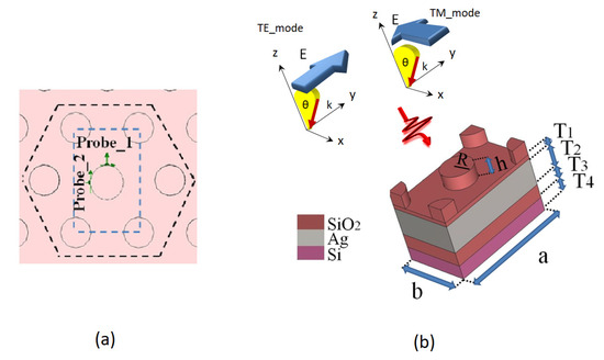
Figure 1.
(a) Top view of the triangular lattice of the SiO2 cylinders forming PPhC in combination with Ag film underneath. Blue dashed line represents the boundary of the unit cell. Local probes that measure the E-field are shown by green dots with arrows; (b) 3D model of the unit cell with the definition of the geometric dimensions and polarizations corresponding to TE and TM modes of the Floquet port.
Reference geometrical parameters of a typical unit cell of the proposed device are listed in Table 1. This unit cell design provides up to a 12-fold enhancement of the local field (see next section for details) around the frequency 560 THz corresponding to the green laser light.

Table 1.
Geometrical characteristics of a unit cell of the proposed structure.
The model of the PPhC with a distributed defect is shown in Figure 2a. In this model, the four optimized unit cells of the infinite PPhC are arranged into a line. The quarters of the SiO2 cylinders at the lower corners of the first unit cell are removed, and the flat layers with thicknesses T1–T4 are extruded in a negative Y direction. The distance from the central cylinder to the edge of the extended multilayer substrate equals Hg/2. Note that for the geometric parameters listed in Table 1, the distance between the rows of dielectric cylinders is 138 nm. Periodic boundary conditions are applied in the X direction, whereas the boundaries at the minimum and maximum of the y-coordinate are electric (Et = 0). These boundary conditions are equivalent to the existence of an additional structure part mirrored. For the normal incident wave with TE polarization, the model in Figure 2a is symmetrically reflected with respect to the y-minimum boundary. The resulting PPhC is shown in Figure 2b and contains the gap between the rows of cylinders of width Hg. This gap is a distributed X-oriented defect in PPhC. A number of field probes are defined into the unit cell with extended defects. Probe_b, Probe_c and Probe_d are similar to the Probe_1 of the unit cell and measure the field amplitudes at the foot of the cylinders. Probe_a is placed at the periodic boundary and measures the E-field amplitude on top of the SiO2 layer between the cylinders, which form the boundary row along the distributed defect.
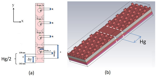
Figure 2.
PPhC with extended defect: (a) Top view with definition of geometric parameters and positions of the E—field probes. (b) Extended 3D model.
3. Results and Discussion
Numerical simulations were conducted by the finite elements method (FEM) implemented into the F-solver of the CST Microwave Studio software. The simulation results for the infinite PPhC unit cell are presented in Figure 3. The model is illuminated by a normally incident plane wave with TE polarization and an E-field amplitude of 1 V/m. The enhancement factor EF is plotted as a function of frequency and unit cell width a, cylinder height h and cylinder radius R. One geometric parameter is swept at a time, whereas others are kept constant and equal to the reference values from Table 1. The shifting of the plasmonic resonance due to the variation of different geometric parameters is clearly seen.
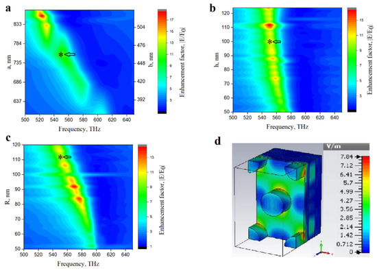
Figure 3.
Enhancement factor as a function of: (a) unit cell width; (a,b) cylinder height h; (c) f cylindrical radius R; (d) amplitude of the E-field on the surface of the unit cell illuminated by a plane wave with the amplitude 1 V/m and TE-polarization. The combination of geometric parameters and the frequency corresponding to this E—field distribution is marked by a star with an arrow in (a–c).
Figure 3d shows the distribution of the E-field amplitude on the surface of the unit cell for the reference design, which is optimized for the frequency 550 THz. The combination of geometric parameters and the frequency corresponding to this distribution is marked by a star with an arrow in Figure 3a–c. It points out our choice of structure dimensions to operate at green laser frequency at normal incidence. The highest field enhancement is created on the surface of the SiO2 layer at the foot of the dielectric cylinder, where EF exceeds 8, whereas between the cylinders EF is less than 4. Figure 4 demonstrates how the position of the plasmonic resonance depends on θ. The highest field enhancement is achieved for normal incidence (θ = 0). Increasing θ shifts the resonant peak to lower frequencies for both the TE and TM modes.
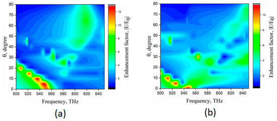
Figure 4.
Enhancement factor versus θ and frequency, (a) for TE-mode measured by Probe_1 and (b) for TM−mode measured by Probe_2.
Local field enhancement in the presence of the distributed gap defect is studied numerically by simulating the model shown in Figure 2a and described earlier. ∆y defined in this figure is the distance from the boundary wall at the y-minimum to the point on the sidewall of the missing cylinder, which is represented by a dashed line in Figure 2a. The width of the defect gap is:
Hg = 2(138 − ∆y)
Figure 5a shows EF at Probe_a as a function of frequency and the parameter ∆y for the structure illuminated by the TE mode. A very sharp distinctive peak with EF = 11 at ∆y = 38 nm and around the frequency 545 THz is clearly seen. The frequency dependences of EF for all the probes are shown in Figure 5b at ∆y = 38 nm. For comparison, the EF of Probe_1 of the reference unit cell (from Figure 5b) is also represented here by the black solid line. Probe_a shows EF close to that of a unit cell and is measured by Probe_1. The main difference is that the high amplitude of the local E-field in the PPhC without a defect is observed in a very small region at the wall of the SiO2 cylinders, whereas an extended defect creates almost similar enhancement in large spots (see Figure 6) between the cylinders along the gap defect. The value of EF at Probe_b, Probe_c and Probe_d decreases with the distance to the gap defect.
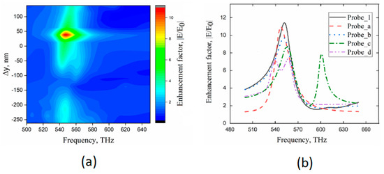
Figure 5.
(a) Local field enhancement measured by Probe_a as a function of frequency and Δy; (b) frequency dependences of EF measured by different probes for the reference unit cell geometric parameters and ∆y = 38 nm.
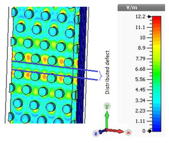
Figure 6.
Close-up of the electric field amplitude at the frequency 545 THz on the surface of PPhC with the optimized gap defect. The structure is excited by a normally incident plane wave of amplitude 1 V/m.
Figure 6 demonstrates the simulated distribution of the E-field on the surface of PPhC with an extended defect. This model is created by the periodic translation of the unit cell from Figure 2a in the x direction with the same boundary conditions, plane wave excitation, reference geometric parameters and Δy = 38 nm. This figure demonstrates that an extended gap defect in PPhC results in the concentration of the E-field in the large spots with 10- to 11-fold local enhancement. The Raman scattering cross-section for the molecules located in these spots may be enhanced by a factor of 1.4*104, as it is proportional to EF4 [1,2]. Long-period oscillations in the y direction are apparently determined by surface waves traveling between the gap defect and the perfectly conducting boundary wall at the maximum and minimum of the y-coordinate. Setting up the electric boundary conditions is equivalent to the addition of mirror extensions to the 3D model shown in Figure 2b at both y-boundaries. As a result, the simulated distribution of the electric field shown in Figure 6 corresponds to the PPhC structure with three x-oriented line defects that are separated from each other by the eight unit cells (see Figure 2a for clarity). As a result, the scattered waves from the line defects interfere with each other and create periodic maxima of the E-field on the surface of PPhC. Due to this interference, the E-field amplitude at the position of Probe_c has two peaks at 550 THz and 600 THz (see Figure 5b). The high amplitude of the E-field at the frequency of plasmonic resonance means that the PPhC is seen by an incident plane wave as a high-impedance surface.
The line defect of the particular width creates a local plasmonic cavity with the maxima of the E-field at its boundaries since the PPhC is a high-impedance surface. This cavity, which can be excited by y-polarized plane waves, is similar to a microwave resonator based on a lambda-half section of a waveguide with open ends. The 12-fold enhancement of the local E-field is defined by the cavity Q-factor that is limited by the loss in Ag film and radiative losses due to the leak of radiation into the surface waves and back-reflection into free space.
4. Conclusions
We have demonstrated and numerically investigated the effect of electric field enhancement in a PPhC along the distributed gap defect, which is created by the violation of translation symmetry rather than PT symmetry. Geometric parameters of the PPhC unit cell consisting of SiO2, Ag, Si layers and a triangular array of SiO2 cylinders are optimized for the local enhancement of the E-field at the frequency 545 THz that corresponds to the wavelength of green laser. The frequency of the maximum enhancement can be tuned by the angle of incidence of the excitation wave. It is shown that the optimized gap defect results in up to 11-fold enhancement of the local E-field amplitude in the spots between the cylinders along the gap defect. Such PPhC may be proposed for applications in SERS, the enhancement of the Purcell factor in quantum systems and nonlinear photonics.
Author Contributions
All authors contributed to the study’s conception. Simulations were performed by B.B. The manuscript was written by A.S.S., B.B. and R.A.K. All authors have read and agreed to the published version of the manuscript.
Funding
The work was supported by the RSCF grant # 22-22-00767.
Data Availability Statement
The datasets analyzed during the current study are available from the corresponding author upon reasonable request.
Conflicts of Interest
The authors declare no conflict of interest.
References
- Sarychev, A.K.; Ivanov, A.; Lagarkov, A.; Barbillon, G. Light concentration by metal-dielectric micro resonators for SERS sensing. Materials 2019, 12, 103. [Google Scholar] [CrossRef] [PubMed]
- Kukushkin, V.; Grishina, Y.V.; Egorov, S.V.; Solov’Ev, V.V.; Kukushkin, I.V. Combined dielectric and plasmon resonance for giant enhancement of Raman scattering. JETP Lett. 2016, 103, 508512. [Google Scholar] [CrossRef]
- Lagarkov, A.; Budashov, I.; Chistyaev, V.; Ezhov, A.; Fedyanin, A.; Ivanov, A.; Kurochkin, I.; Kosolobov, S.; Latyshev, A.; Nasimov, D.; et al. SERS-active dielectric metamaterials based on periodic nanostructures. Opt. Express 2016, 24, 7133–7150. [Google Scholar] [CrossRef] [PubMed]
- Le Ru, E.C.; Blackie, E.; Meyer, M.; Etchegoin, P.G. Surface enhanced Raman scattering enhancement factors: A comprehensive study. J. Phys. Chem. C 2007, 111, 13794. [Google Scholar] [CrossRef]
- Fedotova, Y.; Kukushkin, V.; Solovyev, V.V.; Kukushkin, I.V. Spoof plasmons enable giant Raman scattering enhancement in near-infrared region. Opt. Express 2019, 27, 32578–32586. [Google Scholar] [CrossRef] [PubMed]
- Kukushkin, V.I.; Vankov, A.B.; Kukushkin, I.V. Long-range manifestation of surface-enhanced Raman scattering. JETP Lett. 2013, 98, 64–69. [Google Scholar] [CrossRef]
- Jin, B.; Argyropoulos, C. Enhanced four-wave mixing with nonlinear plasmonic metasurfaces. Sci. Rep. 2016, 6, 28746. [Google Scholar] [CrossRef]
- Smirnova, D.; Leykam, D.; Chong, Y.; Kivshar, Y. Nonlinear topological photonics. Appl. Phys. Rev. 2020, 7, 021306. [Google Scholar] [CrossRef]
- Fedotova, A.; Younesi, M.; Sautter, J.; Vaskin, A.; Lochner, F.J.F.; Steinert, M.; Geiss, R.; Pertsch, T.; Staude, I.; Setzpfandt, F. Second-harmonic generation in resonant nonlinear metasurfaces based on lithium niobate. Nano Lett. 2020, 20, 8608–8614. [Google Scholar] [CrossRef]
- Smirnova, D.; Kruk, S.; Leykam, D.; Melik-Gaykazyan, E.; Choi, D.-Y.; Kivshar, Y. Third-harmonic generation in photonic topological metasurfaces. Phys. Rev. Lett. 2019, 123, 103901. [Google Scholar] [CrossRef]
- Yuan, Q.; Gu, L.; Fang, L.; Gan, X.; Chen, Z.; Zhao, J. Giant enhancement of nonlinear harmonic generation in a silicon topological photonic crystal nanocavity chain. Laser Photonics Rev. 2022, 16, 2100269. [Google Scholar] [CrossRef]
- Butet, J.; Brevet, P.-F.; Martin, O.J.F. Optical second harmonic generation in plasmonic nanostructures: From fundamental principles to advanced applications. ACS Nano 2015, 9, 10545–10562. [Google Scholar] [CrossRef]
- Bandres, M.A.; Wittek, S.; Harari, G.; Parto, M.; Ren, J.; Segev, M.; Christodoulides, D.N.; Khajavikhan, M. Topological insulator laser: Experiments. Science 2018, 359, eaar4005. [Google Scholar] [CrossRef]
- You, J.W.; Lan, Z.; Panoiu, N.C. Four-wave mixing of topological edge plasmons in graphene metasurfaces. Sci. Adv. 2020, 6, eaaz3910. [Google Scholar] [CrossRef]
- Barik, S.; Karasahin, A.; Flower, C.; Cai, T.; Miyake, H.; DeGottardi, W.; Hafezi, M.; Waks, E. A topological quantum optics interface. Science 2018, 359, 666–668. [Google Scholar] [CrossRef]
- Barik, S.; Miyake, H.; DeGottardi, W.; Waks, E.; Hafezi, M. Two-dimensionally confined topological edge states in photonic crystals. New J. Phys. 2016, 18, 113013. [Google Scholar] [CrossRef]
- He, X.-T.; Liang, E.-T.; Yuan, J.-J.; Qiu, H.-Y.; Chen, X.-D.; Zhao, F.-L.; Dong, J.-W. A silicon-on-insulator slab for topological valley transport. Nat. Commun. 2019, 10, 872. [Google Scholar] [CrossRef]
- Yang, Y.; Jiang, H.; Hang, Z.H. Topological valley transport in two-dimensional honeycomb photonic crystals. Sci. Rep. 2018, 8, 1588. [Google Scholar] [CrossRef]
- Barik, S.; Karasahin, A.; Mittal, S.; Waks, E.; Hafezi, M. Chiral quantum optics using a topological resonator. Phys. Rev. B 2020, 101, 205303. [Google Scholar] [CrossRef]
- Ota, Y.; Liu, F.; Katsumi, R.; Watanabe, K.; Wakabayashi, K.; Arakawa, Y.; Iwamoto, S. Photonic crystal nanocavity based on a topological corner state. Optica 2019, 6, 786–789. [Google Scholar] [CrossRef]
- El Hassan, A.; Kunst, F.K.; Moritz, A.; Andler, G.; Bergholtz, E.J.; Bourennane, M. Corner states of light in photonic waveguides. Nat. Photonics 2019, 13, 697–700. [Google Scholar] [CrossRef]
- Palik, E.D. Handbook of Optical Constants of Solids, 3rd ed.; Academic Press: Cambridge, MA, USA, 1998. [Google Scholar]


Disclaimer/Publisher’s Note: The statements, opinions and data contained in all publications are solely those of the individual author(s) and contributor(s) and not of MDPI and/or the editor(s). MDPI and/or the editor(s) disclaim responsibility for any injury to people or property resulting from any ideas, methods, instructions or products referred to in the content. |
© 2023 by the authors. Licensee MDPI, Basel, Switzerland. This article is an open access article distributed under the terms and conditions of the Creative Commons Attribution (CC BY) license (https://creativecommons.org/licenses/by/4.0/).