Abstract
Compact waveguide crossing is a fundamental component of optoelectronic fusion chip solutions due to its orders-of-magnitude smaller footprint than that of conventional photonic integrated circuits. In this paper, we suggest 2 × 2 compact silicon-on-silica waveguides that can implement all of the fundamental Boolean logic functions, including XOR, AND, OR, NOT, NOR, XNOR, and NAND, operated at 1.55 μm. Three input waveguides, one output waveguide, and a design area compose the proposed waveguide. The execution of the specified logic gates relies on the constructive and destructive interferences produced by the phase variations between the input beams. The contrast ratio (CR) is employed as a performance metric to assess how well these logic functions operate. In comparison to other reported designs, the proposed waveguide achieves higher CRs at a high speed of 120 Gb/s.
1. Introduction
The need for computational resources has grown significantly in today’s information society, and the density of conventional integrated circuit transistors is reaching its physical limit. In the past decade, there has been considerable growth in the field of integrated photonics, particularly in the area of silicon photonics, due to the high transmission efficiency, low power consumption, affordable and dense integration, and compatibility with complementary metal–oxide–semiconductor (CMOS) manufacturing processes [1]. Since the inception of silicon photonics in the telecommunications industry, many applications that are based on this platform have grown to include sensing, optomechanics, nonlinear optics, quantum optics, and even neuroscience. On the other hand, optoelectronic and photonic devices and circuits based on silicon-on-insulator (SOI) are appealing because they can be fabricated using the CMOS process and have the potential for monolithic integration on CMOS chips. SOI is produced by depositing a thin layer of crystalline silicon on a silica (silicon dioxide) insulating layer. Moreover, the SOI waveguide crossing is a crucial device unit to create a variety of implementation schemes, such as shaped taper waveguide crossing [2,3,4,5], multimode interferometers [6,7,8], and photonic crystal waveguide crossing [9,10]. However, low insertion loss was reported using these structures, especially in 2 × 2 [2], but large crossings are unattractive for large-scale photonic interconnects. All-optical Boolean functions, on the other hand, are essential elements for information optical processing because they efficiently overcome the fundamental restrictions of their electronic equivalents, particularly the constrained data transfer speed and bandwidth. Recently, a variety of optical waveguides have been employed to implement all-optical Boolean functions [11,12,13,14,15,16,17,18,19,20,21,22]. However, the majority of these described devices have used photonic crystal structures or are constructed from noble costly metals to implement only one, or at most two, logic operations. Furthermore, these reported schemes necessitate highly accurate and advanced microfabrication technologies. Due to these impediments, it is still difficult to implement multifunctional logic functions with high performance using simple and inexpensive waveguides. Therefore, in this paper, we propose compact 2 × 2 silicon-on-silica waveguides to realize seven basic Boolean logic functions, i.e., XOR, AND, OR, NOT, NOR, XNOR, and NAND, operated at the 1.55 μm telecommunications wavelength. The proposed waveguide consists of three input waveguides, one output waveguide, and a design area. Based on the constructive and destructive interference produced by the phase differences between the input beams, the considered logic functions operate. By employing Lumerical finite-difference-time-domain (FDTD) simulation tools, the contrast ratio (CR) is calculated to evaluate how effectively the logic functions work. Through comparison of the outcomes with other reported designs [11,12,13,14,15,16,17,18,19,20,21,22], it is shown that the proposed design exhibits higher CRs at a high speed of 120 Gb/s.
2. 2 × 2 Silicon Waveguide
The proposed waveguide comprises a silicon core that is printed on a silica substrate as cladding, which is advantageous for controlling the size of optical devices as well as for linear and nonlinear applications [1]. This waveguide has three input ports that are open to transverse electric mode polarized waves, one output port, and a design area. The design area measures 2 μm by 0.6 μm, the top and lower arms are separated by 4 μm, and the width of the input and output arms are both set to 0.4 μm. The coupling gap between the top and lower arms is 0.1 μm, and the bend radius is 2 μm. The total waveguide cross-section area is 6 × 4.8 μm2. The input beams have the same wavelength and intensity. A schematic diagram of the 2 × 2 silicon waveguide and the light field distributions are displayed in Figure 1.
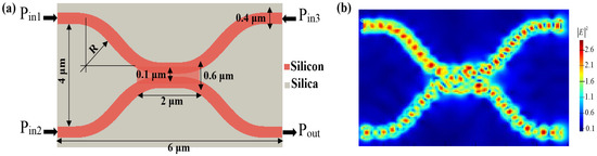
Figure 1.
(a) Schematic diagram and (b) light field distributions of 2 × 2 silicon waveguide.
The threshold transmission (Tth) value is initially set to 0.14, which is the minimum normalized power required to generate the spectral transmission (T). , where is the intensity at Pout and is the sum of the intensities at three input ports [15]. The intensity monitors of the FDTD are set to record the simulation findings. The logic output is ‘1’ when T > Tth; otherwise, the output is ‘0’ (i.e., T < Tth). The incident beams must match in phase to maximize T. The destructive interference scatters the incident beams when the phases of the incident beams are out of phase with the waveguide, producing a ‘0’ output. The CR described by [19,20], where and are the mean peak powers of outputs ‘1’ and ‘0’, respectively, is employed to evaluate the performance of the considered logic functions better and more accurately than other metrics [23].
Figure 2 depicts the spectral transmission (T) and the loss versus the operating wavelength (λ) when the input beams are injected at the three input ports with the same phase of 0°. Due to the constructive interference between the input beams utilizing the suggested waveguide, a high T of 0.865 and a low loss of 0.63 dB/μm are achieved. The scattering at the interfaces between the slots and the design area and the material absorption are responsible for these negligible propagation losses. Moreover, this graph demonstrates that our waveguide generates a high T and a low loss across the entire range of exploitable telecommunication wavelengths, i.e., 1.3–1.6 μm.
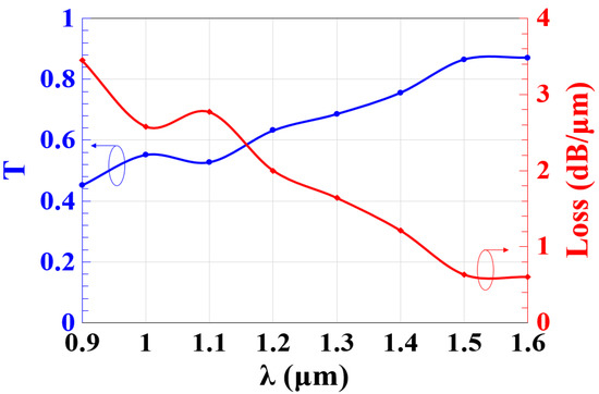
Figure 2.
Spectral transmission (T) and loss versus operating wavelength (λ) utilizing 2 × 2 silicon waveguide.
The design area, which controls the coupling gap between the upper and the lower waveguide’s arms, is essential for the suggested design to achieve the considered logic functions with high CRs. Therefore, Figure 3 illustrates the simulation of the effect of the design area’s volume on the normalized spectral transmission (T) at 1.55 μm. This figure shows that the maximum T occurs between 0.40 and 0.60 μm3, which gives flexibility in the practical implementation of the suggested design. A closer look at this figure reveals that by varying the design area’s volume, the light scattering and absorption within the materials increase, which, in turn, causes higher losses.
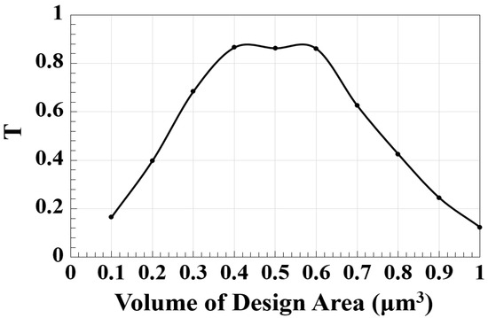
Figure 3.
Spectral transmission (T) versus volume of design area utilizing 2 × 2 silicon waveguide at 1.55 μm.
The process variations, such as those in waveguide thickness, etching depth, waveguide width, and material refractive indices, result in phase errors that introduce uncertainty in the responses of photonic devices [24,25,26]. Therefore, it is necessary to study the effect of the phase error on the performance of the logic operations. Figure 4 shows the dependence of the normalized spectral transmission (T) on the phase error utilizing the 2 × 2 silicon waveguide at 1.55 μm. This figure shows that by increasing the amount of phase error, T is decreased, which, in turn, reduces the CR.
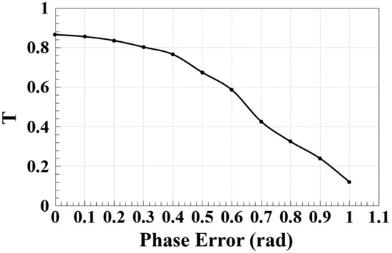
Figure 4.
Spectral transmission (T) versus phase error utilizing 2 × 2 silicon waveguide at 1.55 μm.
The top and lower waveguide arms are separated by a gap of 4 μm. This gap plays a central role in the waveguide performance. Therefore, Figure 5 shows the relation between the spectral loss and the gap between the waveguide arms utilizing the proposed 2 × 2 waveguide crossing at 1.55 μm. It can be seen that the loss deteriorates with the widening of the separated gap. This happens because if the separated gap is increased, the upper and lower waveguide arms move away from their convergence point at the design area, which induces no interferences between the incoming beams, and thus naturally results in a loss increase.
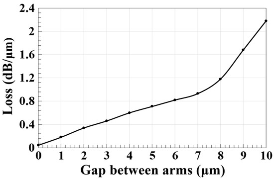
Figure 5.
Spectral loss versus gap between waveguide arms utilizing 2 × 2 silicon waveguide at 1.55 μm.
The bending radiation losses are caused by the coupling of light from core modes to cladding modes when the optical waveguides/fibers are bent. These losses must be simulated correctly as they critically affect the device’s performance. Therefore, Figure 6 shows the bending loss as a function of the bend radius (R) using the proposed waveguide at 1.55 μm. The form of the obtained curve agrees well with the trend that bending losses increase for smaller R. Accurate measurements of bending losses in silicon waveguides with submicron dimensions fabricated on SOI wafers that experimentally verify this fact are reported in [27,28].
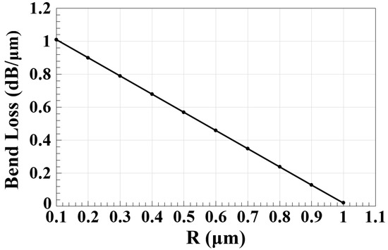
Figure 6.
Bending radiation loss versus bend radius (R) utilizing 2 × 2 silicon waveguide at 1.55 μm.
Realizing a highly flat and low dispersion over a broad wavelength range is a key challenge for integrated waveguides. Dispersion flattening has proven to be a challenge for silicon waveguides due to the tight light confinement and severe waveguide dispersion in the highly nonlinear integrated waveguides. Additionally, it may be advantageous to reduce phase mismatching and eliminate the need for high pump power in nonlinear processes by optimizing the dispersion profile in silicon waveguides [29]. The transverse size of silicon strip and rib waveguides would need to be quite large to produce one zero-dispersion wavelength in the desired wavelength range, which is typically around 1.55 μm [30,31]. The waveguide dispersion [32] is decreased with the increase in the operating wavelength (λ), as shown in Figure 7. The proposed 2 × 2 silicon waveguide achieves a low dispersion of 0.54 ps2/m at 1.55 μm and also exhibits flattened dispersion from the 1.45 to 1.6 μm wavelength, which is potentially useful for both telecom and mid-infrared applications. The device’s performance can be optimized through the control of the waveguide dispersion by varying the waveguide’s geometry [32].
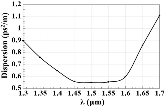
Figure 7.
Waveguide dispersion versus operating wavelength (λ) utilizing 2 × 2 silicon waveguide.
3. Logic Functions
3.1. XOR
For the XOR, AND, and OR operations to be implemented, a reference beam (REF) needs to be inserted into Pin3 of Figure 1. A reference phase difference between the input beams is introduced using the REF (all ‘1’s), which can produce either constructive or destructive interference. Two additional beams are supplied to Pin1 and Pin2, respectively. Pout generates a logical ‘1’ as a result of the constructive interference between the input beams when Pin1 and Pin2 are ‘0’ and ‘1’, or vice versa (i.e., 01 or 10), with REF adjusted at the same phase of 0°. Due to destructive interference between the input beams, Pout results in a ‘0’ when both Pin1 and Pin2 are ‘1’ launched at θ1 = 180° and θ2 = 90° with REF at θREF = 0°. The XOR gate is then implemented between the two input beams. The distributions of the light fields for the logic XOR gate at 1.55 μm are shown in Figure 8.
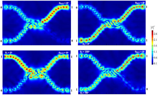
Figure 8.
Light field distributions for XOR function utilizing 2 × 2 silicon waveguide at 1.55 μm.
The considerable disparity between and allows the proposed waveguide to have a high CR = 39.64 dB. The simulation findings for the XOR function are provided in Table 1.

Table 1.
Simulation findings for XOR (Tth = 0.14).
3.2. AND
By connecting two beams to Pin1 and Pin2, as well as the REF (all ‘1’s) to Pin3, the AND function is performed (see Figure 1). The phase angle of REF is adjusted to θREF = 0°. Destructive interference manifests because of the phase difference between the input beams when the two beams ‘1’ and ‘0’, or vice versa (i.e., 01 or 10), are injected at a different phase than the REF phase, leading to an output of ‘0’. Because the input beams and REF have the same phase, i.e., θ1 = θ2 = θREF = 0°, constructive interference produces ‘1′’ at Pout when both input beams are ‘1’. The AND logic operation is therefore functionally accomplished. Figure 9 displays the light field distributions for the logic AND gate at 1.55 μm.
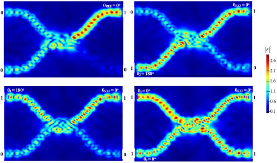
Figure 9.
Light field distributions for AND function utilizing 2 × 2 silicon waveguide at 1.55 μm.
The simulation findings for the AND function with CR = 31 dB are summarized in Table 2.
Table 2.
Simulation findings for AND (Tth = 0.14).
3.3. OR
Two beams are sent into the waveguide from Pin1 and Pin2, respectively, while the REF is supplied from Pin3, similar to the XOR and AND operations. When all input beams propagate at the same phase, i.e., θ1 = θ2 = θREF = 0°, the OR function can be straightforwardly achieved, yielding a ‘1’ output as a result of constructive interference between the input beams. Utilizing a 2 × 2 silicon waveguide at 1.55 μm, Figure 10 displays the light field distributions for the logic OR function.
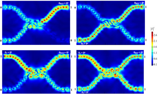
Figure 10.
Light field distributions for OR function utilizing 2 × 2 silicon waveguide at 1.55 μm.
The simulation findings for the OR function at 1.55 μm concerning T and CR are summarized in Table 3. A high CR = 42.75 dB is achieved by utilizing the proposed waveguide due to the wide gap between and .
Table 3.
Simulation findings for OR (Tth = 0.14).
Table 4 compares the simulation findings of the considered logic functions at 1.55 μm using the proposed waveguide with and without REF. The obtained CRs are much greater with than without REF, according to the cited data.
Table 4.
CR without and with REF.
3.4. NOT
A clock light (Clk) and an input beam are, respectively, sent into the proposed waveguide from Pin1 and Pin2 in Figure 1 to perform the NOT function. In a manner, and similar to REF, the Clk introduces an additional phase shift to the propagating beams, altering the waveguide balance and producing the desired output. To achieve this function, the phases of the Clk (all ‘1’s) and input beam should be adjusted at θClk = 180° and θ2 = 0°, respectively. The input beams suffer different phases when Pin2 is set to ‘1’, inducing destructive interference and producing a logical ‘0’ output (i.e., T < Tth). The Clk does not go through a differencing phase when Pin2 is set to ‘0’, producing a logical ‘1’ output (i.e., T > Tth) at Pout. Thus, the NOT function is realized. Figure 11 depicts the NOT function’s light field distributions at 1.55 μm.
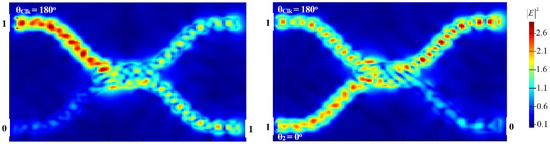
Figure 11.
Light field distributions for NOT function utilizing 2 × 2 silicon waveguide at 1.55 μm.
The simulation findings for the NOT function are listed in Table 5. These findings demonstrate that a NOT logic function at 1.55 μm with CR = 24.63 dB can be formed utilizing the suggested waveguide.
Table 5.
Simulation findings for NOT (Tth = 0.14).
3.5. NOR
The Clk beam is injected into Pin1 to realize the NOR (NOT–OR) function, while the other two beams are injected into Pin2 and Pin3, respectively (see Figure 1). A logical ‘0’ is produced at Pout due to the destructive interference when the combination of (01, 10, or 11) OF the input beams is injected at various angles. If the (00) combination of the two beams is launched, the Clk beam with θClk = 180° will cancel the phase balance of the three input ports, thereby resulting in a logical ‘1’ at Pout. Thus, the NOR gate is created, as seen in Figure 12.
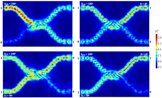
Figure 12.
Light field distributions for NOR function utilizing 2 × 2 silicon waveguide at 1.55 μm.
Table 6 provides a summary of the simulation findings for the NOR gate with CR = 25.53 dB.
Table 6.
Simulation findings for NOR (Tth = 0.14).
3.6. NAND
It is possible to perform the NAND (NOT–AND) operation by injecting the Clk into Pin1 and the other two beams into Pin2 and Pin3, respectively. Due to the Clk’s θClk = 180°, the output is ‘1’ when Pin2 and Pin3 are ‘OFF’ (i.e., 00). Constructive interference occurs when (01, 10) is launched with Clk at the same angle of 180°, producing a ‘1’ at the output. When (11) is launched with Clk at different phases, i.e., θClk = 180°, θ2 = 90°, and θ3 = 0°, as shown in Figure 13, the concomitant destructive interference results in a ‘0’ at the output.
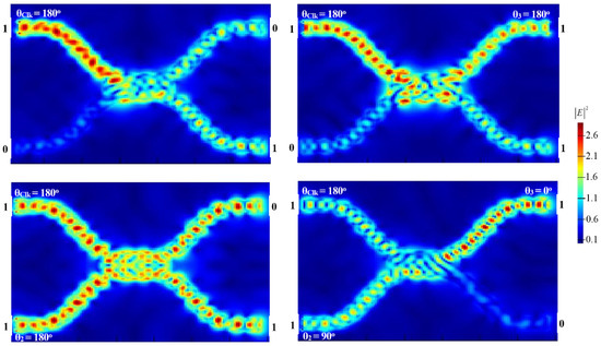
Figure 13.
Light field distributions for NAND function utilizing 2 × 2 silicon waveguide at 1.55 μm.
The findings of the NAND function are compiled in Table 7. The mean peak power of ‘1’ is greater than ‘0’ when using our design at 1.55 μm, enabling a high CR = 33.38 dB for the NAND function.
Table 7.
Simulation findings for NAND (Tth = 0.14).
3.7. XNOR
The Clk enters Pin1, and the two additional beams are injected from Pin2 and Pin3, similarly to the NOR and NAND functions, to carry out the XNOR (exclusive-NOR) function. When the input beam combination (11) is introduced along with the Clk at the same phase of 180°, Pout produces a ‘1’ output due to constructive interference. The Clk at 180° produces a ‘1’ output for the (00) combination. As depicted in Figure 14, Pout comprises a ‘0’ when the beam combinations (01) or (10) are injected with a different phase.
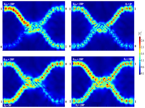
Figure 14.
Light field distributions for XNOR function utilizing 2 × 2 silicon waveguide at 1.55 μm.
A high CR = 26 dB for the XNOR function is achieved employed the proposed waveguide. The XNOR simulation findings are provided in Table 8.
Table 8.
Simulation findings for XNOR (Tth = 0.14).
The working data rate of the proposed waveguide is calculated to be 120 Gb/s for an optical bandwidth of 30 GHz and four beam levels (i.e., 00, 01, 10, 11) according to the Nyquist formula [33].
The manufacturing constraints are often referred to as a bottleneck. As more applications rely on nanophotonic devices, photonic design is becoming increasingly challenging and sophisticated. Designers are increasingly turning to advanced optimization techniques rather than traditional photonic design methodologies to address this challenge [34,35,36,37]. These new techniques examine devices with totally arbitrary geometries rather than modifying relatively straightforward known geometries with a small number of parameters, as is the conventional practice. In order to take advantage of the extra degrees of freedom, devices have been created that have incredibly small footprints, high efficiency, and innovative features that cannot be accomplished using conventional techniques [38,39,40,41,42,43,44,45,46]. The silicon and silica utilized in the proposed waveguide are common in the Earth’s crust and play a significant role in the composition of the mantle. Because the nanofabrication technologies are already in place, it would, therefore, be possible to implement the proposed waveguide based on the key outcomes of the conducted simulation. In fact, it has been reported that several Boolean logic functions can be implemented experimentally based on different waveguides [16,22,47,48,49].
In order to check whether our work contributes in advancing the relevant the state-of-art, we compared our principal outcomes on the realization of the target logic functions using the proposed waveguides with those of other designs employed for the same purpose. To this end, we constructed Table 9, whose inspection reveals that, in contrast to other reported designs, the suggested waveguides allow for the performance of the specified logic functions at 1550 nm with higher CRs.
Table 9.
Evaluation of the proposed design in comparison to other published waveguide-based logic functions.
4. Conclusions
We have designed a full family of fundamental Boolean logic functions operated at 1.55 μm, using compact 2 × 2 silicon-on-silica waveguides. The proposed scheme consists of three input waveguides, one output waveguide, and a design area. Lumerical FDTD analysis software was used to perform these logic functions. The key for the proper operation of these functions is inducing and exploiting the appropriate tuning of the phase angle of the input-launched beams. By conducting numerical simulations based on FDTD analysis, we assessed and verified the high performance of the target gates. Moreover, we compared our outcomes to those of other reported similar designs and confirmed that the proposed waveguide results in higher CRs at higher operating speeds of up to 120 Gb/s.
Author Contributions
Conceptualization, A.K.; data curation, A.K.; formal analysis, A.K.; funding acquisition, A.K.; investigation, A.K. and K.E.Z.; methodology, A.K. and K.E.Z.; project administration, A.K.; resources, A.K.; software, A.K.; supervision, K.E.Z.; writing—original draft, A.K.; writing—review and editing, A.K. and K.E.Z. All authors have read and agreed to the published version of the manuscript.
Funding
This research received no external funding.
Institutional Review Board Statement
Not applicable.
Informed Consent Statement
Not applicable.
Data Availability Statement
Not applicable.
Acknowledgments
A.K. expresses gratitude for the support provided by the Chinese Academy of Sciences President’s International Fellowship Initiative (Grant No. 2022VMB0013).
Conflicts of Interest
The authors declare no conflict of interest.
References
- Tong, X.C. Silicon-on-Insulator Waveguides. In Advanced Materials for Integrated Optical Waveguides; Springer Series in Advanced Microelectronics; Springer: Berlin/Heidelberg, Germany, 2014; Volume 46, pp. 253–287. [Google Scholar]
- Peng, Z.; Feng, J.; Du, T.; Cheng, W.; Wang, Y.; Zang, S.; Cheng, H.; Ren, X.; Shuai, Y.; Liu, H.; et al. Series of ultra-low loss and ultra-compact multichannel silicon waveguide crossing. Opt. Express 2022, 30, 27366–27380. [Google Scholar] [CrossRef] [PubMed]
- Ma, Y.; Zhang, Y.; Yang, S.; Novack, A.; Ding, R.; Lim, A.E.; Lo, G.; Baehr-Jones, T.; Hochberg, M. Ultralow loss single layer submicron silicon waveguide crossing for SOI optical interconnect. Opt. Express 2013, 21, 29374–29382. [Google Scholar] [CrossRef] [PubMed]
- Sanchis, P.; Villalba, P.; Cuesta, F.; Håkansson, A.; Griol, A.; Galán, J.V.; Brimont, A.; Martí, J. Highly efficient crossing structure for silicon-on-insulator waveguides. Opt. Lett. 2009, 34, 2760–2762. [Google Scholar] [CrossRef] [PubMed]
- Bogaerts, W.; Dumon, P.; Thourhout, D.V.; Baets, R. Low-loss, low-cross-talk crossings for silicon-on-insulator nanophotonic waveguides. Opt. Lett. 2007, 32, 2801–2803. [Google Scholar] [CrossRef]
- Brunetti, G.; Marocco, G.; Benedetto, A.D.; Agostino Giorgio, A.; Mario Nicola Armenise, M.N.; Ciminelli, C. Design of a large bandwidth 2 × 2 interferometric switching cell based on a sub-wavelength grating. J. Opt. 2021, 23, 085801. [Google Scholar] [CrossRef]
- Chang, W.; Lu, L.; Ren, X.; Lu, L.; Cheng, M.; Liu, D.; Zhang, M. An ultracompact multimode waveguide crossing based on subwavelength asymmetric Y-junction. IEEE Photonics J. 2018, 10, 1–8. [Google Scholar] [CrossRef]
- Chen, C.H.; Chiu, C.H. Taper-integrated multimode-interference based waveguide crossing design. IEEE J. Quantum Electron. 2010, 46, 1656–1661. [Google Scholar] [CrossRef]
- Gilarlue, M.; Badri, S.H. Photonic crystal waveguide crossing based on transformation optics. Opt. Commun. 2019, 450, 308–315. [Google Scholar] [CrossRef]
- Lu, L.; Zhang, M.; Zhou, F.; Chang, W.; Tang, J.; Li, D.; Ren, X.; Pan, Z.; Cheng, M.; Liu, D. Inverse-designed ultra-compact star-crossings based on PhC-like subwavelength structures for optical intercross connect. Opt. Express 2017, 25, 18355–18364. [Google Scholar] [CrossRef]
- Priya, N.H.; Swarnakar, S.; Krishna, S.V.; Kumar, S. Design and analysis of an optical three-input AND gate using a photonic crystal fiber. Appl. Opt. 2022, 61, 77–83. [Google Scholar]
- Priya, N.H.; Swarnakar, S.; Krishna, S.V.; Kumar, S. Design and analysis of a photonic crystal-based all-optical 3-input OR gate for high-speed optical processing. Opt. Quantum Electron. 2021, 53, 720. [Google Scholar] [CrossRef]
- Rao, D.G.S.; Swarnakar, S.; Palacharla, V.; Raju, K.S.R.; Kumar, S. Design of all-optical AND, OR, and XOR logic gates using photonic crystals for switching applications. Photonic Netw. Commun. 2021, 41, 109–118. [Google Scholar] [CrossRef]
- Rani, P.; Kalra, Y.; Sinha, R.K. Design of all optical logic gates in photonic crystal waveguides. Optik 2015, 126, 950–955. [Google Scholar] [CrossRef]
- Yao, C.; Kotb, A.; Wang, B.; Singh, S.; Guo, C. All-optical logic gates using dielectric-loaded waveguides with quasi-rhombus metasurfaces. Opt. Lett. 2020, 45, 3769–3772. [Google Scholar] [CrossRef]
- Pan, D.; Wei, H.; Xu, H. Optical interferometric logic gates based on metal slot waveguide network realizing whole fundamental logic operations. Opt. Express 2013, 21, 9556. [Google Scholar] [CrossRef]
- Bian, Y.; Gong, Q. Compact all-optical interferometric logic gates based on one-dimensional metal-insulator-metal structures. Opt. Commun. 2014, 313, 27–35. [Google Scholar] [CrossRef]
- Al-Musawi, H.K.; Al-Janabi, A.K.; Al-Abassi, S.A.W.; Abusiba, N.A.A.; Al-Fatlawi, N.A.Q. Plasmonic logic gates based on dielectric-metal-dielectric design with two optical communication bands. Optik 2020, 223, 165416. [Google Scholar] [CrossRef]
- Kotb, A.; Zoiros, K.E.; Li, W. Silicon-on-silica waveguides-based all-optical logic gates at 1.55 μm. Phys. Scr. 2023, 98, 035517. [Google Scholar] [CrossRef]
- Kotb, A.; Zoiros, K.E. K-shaped silicon waveguides for logic operations at 1.55 μm. Electronics 2022, 11, 3748. [Google Scholar] [CrossRef]
- Neseli1, B.; Yilmaz, Y.A.; Kurt, H.; Turduev, M. Inverse design of ultra-compact photonic gates for all-optical logic operations. J. Phys. D Appl. Phys. 2022, 55, 215107. [Google Scholar] [CrossRef]
- Kita, S.; Nozaki, K.; Takata, K.; Shinya, A.; Notomi, M. Ultrashort low-loss Ψ gates for linear optical logic on Si photonics platform. Commun. Phys. 2020, 3, 33. [Google Scholar] [CrossRef]
- Zoiros, K.E.; Papadopoulos, G.; Houbavlis, T.; Kanellos, G.T. Theoretical analysis and performance investigation of ultrafast all-optical Boolean XOR gate with semiconductor optical amplifier-assisted Sagnac interferometer. Opt. Commun. 2006, 258, 114–134. [Google Scholar] [CrossRef]
- Han, Q.; Robin, D.; Gervais, A.; Ménard, M.; Shi, W. Phase errors and statistical analysis of silicon-nitride arrayed waveguide gratings. Opt. Express 2022, 30, 42784–42800. [Google Scholar] [CrossRef] [PubMed]
- Khan, U.; Fiers, M.; Xing, Y.; Bogaerts, W. Experimental phase error extraction and modelling in silicon photonic arrayed waveguide gratings. Proc. SPIE 2020, 11285, 1128510. [Google Scholar]
- Goh, T.; Suzuki, S.; Sugita, A. Estimation of waveguide phase error in silica-based waveguides. J. Light. Technol. 1997, 15, 2107–2113. [Google Scholar] [CrossRef]
- Vlasov, Y.A.; McNab, S.J. Losses in single-mode silicon-on-insulator strip waveguides and bends. Opt. Express 2004, 12, 1622–1631. [Google Scholar] [CrossRef]
- Bienstman, P.; Six, E.; Roelens, M.; Vanwolleghem, M.; Baets, R. Calculation of bending losses in dielectric waveguides using eigenmode expansion and perfectly matched layers. IEEE Photonics Technol. Lett. 2002, 14, 164–166. [Google Scholar] [CrossRef]
- Zhang, L.; Yue, Y.; Beausoleil, R.C.; Willner, A.E. Flattened dispersion in silicon slot waveguides. Opt. Express 2010, 18, 20529–20534. [Google Scholar] [CrossRef]
- Yin, L.; Lin, Q.; Agrawal, G.P. Dispersion tailoring and soliton propagation in silicon waveguides. Opt. Lett. 2006, 31, 1295–1297. [Google Scholar] [CrossRef]
- Dadap, J.I.; Panoiu, N.C.; Chen, X.; Hsieh, I.W.; Liu, X.; Chou, C.Y.; Dulkeith, E.; McNab, S.J.; Xia, F.; Green, W.M.J.; et al. Nonlinear-optical phase modification in dispersion engineered Si photonic wires. Opt. Express 2008, 16, 1280–1299. [Google Scholar] [CrossRef]
- Hu, Y.; Yang, Z.; Chen, N.; Hu, H.; Zhang, B.; Yang, H.; Lu, X.; Zhang, X.; Xu, J. 3 X 40 Gbit/s all-optical logic operation based on low-loss triple-mode silicon waveguide. Micromachines 2022, 13, 90. [Google Scholar] [CrossRef]
- Crisp, J.; Elliott, B. Introduction to Fiber Optics, 3rd ed.; Elsevier: Amsterdam, The Netherlands, 2005. [Google Scholar]
- Vercruysse, D.; Sapra, N.V.; Su, L.; Trivedi, R.; Vučković, J. Analytical level set fabrication constraints for inverse design. Sci. Rep. 2019, 9, 8999. [Google Scholar] [CrossRef]
- Sean Molesky, S.; Zin Lin, Z.; Alexander, Y.; Piggott, A.Y.; Weiliang Jin, W.; Vucković, J.; Rodriguez, A.W. Outlook for inverse design in nanophotonics. Nat. Photonics 2018, 12, 659–670. [Google Scholar] [CrossRef]
- Lu, J.; Vuckovic, J. Nanophotonic Computational Design. Opt. Express 2013, 21, 7748–7759. [Google Scholar] [CrossRef]
- Jensen, J.S.; Sigmund, O. Topology optimization for nano-photonics. Laser Photonics Rev. 2011, 5, 308–321. [Google Scholar] [CrossRef]
- Shen, B.; Wang, P.; Polson, R.; Menon, R. Integrated metamaterials for efficient and compact free-space-to-waveguide coupling. Opt. Express 2014, 22, 27175–27182. [Google Scholar] [CrossRef]
- Piggott, A.Y.; Lu, J.; Lagoudakis, K.G.; Petykiewicz, J.; Babinec, T.M.; Vučković, J. Inverse design and demonstration of a compact and broadband on-chip wavelength demultiplexer. Nat. Photonics 2015, 9, 374–377. [Google Scholar] [CrossRef]
- Shen, B.; Wang, P.; Polson, R.; Menon, R. An integrated-nanophotonics polarization beam splitter with 2.4 × 2.4 μm2 footprint. Nat. Photonics 2015, 9, 378–382. [Google Scholar] [CrossRef]
- Sell, D.; Yang, J.; Doshay, S.; Yang, R.; Fan, J.A. Large-Angle, Multifunctional Metagratings Based on Freeform Multimode Geometries. Nano Lett. 2017, 17, 3752–3757. [Google Scholar] [CrossRef]
- Yu, Z.; Cui, H.; Sun, X. Genetically optimized on-chip wideband ultracompact refectors and Fabry–Perot cavities. Photonics Res. 2017, 5, B15–B19. [Google Scholar] [CrossRef]
- Su, L.; Piggott, A.Y.; Sapra, N.V.; Petykiewicz, J.; Vučković, J. Inverse Design and Demonstration of a Compact on-Chip Narrowband Tree-Channel Wavelength Demultiplexer. ACS Photonics 2018, 5, 301–305. [Google Scholar] [CrossRef]
- Sitawarin, C.; Jin, W.; Lin, Z.; Rodriguez, A.W. Inverse-designed photonic fbers and metasurfaces for nonlinear frequency conversion. Photonics Res. 2018, 6, 82–89. [Google Scholar] [CrossRef]
- Pestourie, R.; Pérez-Arancibia, C.; Lin, Z.; Shin, W.; Capasso, F.; Johnson, S.G. Inverse design of large-area metasurfaces. Opt. Express 2018, 26, 33732–33747. [Google Scholar] [CrossRef] [PubMed]
- Wang, J.; Shi, Y.; Hughes, T.; Zhao, Z.; Fan, S. Adjoint-based optimization of active nanophotonic devices. Opt. Express 2018, 26, 3236–3248. [Google Scholar] [CrossRef]
- Gao, L.; Chen, L.; Wei, H.; Xu, H. Lithographically fabricated gold nanowire waveguides for plasmonic routers and logic gates. Nanoscale 2018, 10, 14771. [Google Scholar] [CrossRef]
- Donzella, V.; Sherwali, A.; Flueckiger, J.; Grist, S.M.; Fard, S.T.; Chrostowski, L. Design and fabrication of SOI micro-ring resonators based on sub-wavelength grating waveguides. Opt. Express 2015, 23, 4791–4803. [Google Scholar] [CrossRef]
- Fu, Y.; Hu, X.; Lu, C.; Yue, S.; Yang, H.; Gong, Q. All-optical logic gates based on nanoscale plasmonic slot waveguides. Nano Lett. 2012, 12, 5784–5790. [Google Scholar] [CrossRef]
Disclaimer/Publisher’s Note: The statements, opinions and data contained in all publications are solely those of the individual author(s) and contributor(s) and not of MDPI and/or the editor(s). MDPI and/or the editor(s) disclaim responsibility for any injury to people or property resulting from any ideas, methods, instructions or products referred to in the content. |
© 2023 by the authors. Licensee MDPI, Basel, Switzerland. This article is an open access article distributed under the terms and conditions of the Creative Commons Attribution (CC BY) license (https://creativecommons.org/licenses/by/4.0/).