Article

Optimal I–V Curve Scan Time for a GaAs Laser Power Converter

1
Laboratory of Optoelectronics and Sensor (OES Lab), School of Science, Hubei University of Technology, Wuhan 430068, China
2
Hubei Engineering Technology Research Center of Energy Photoelectric Device and System, Hubei University of Technology, Wuhan 430068, China
3
AOV Energy LLC, Wuhan 430068, China
*
Authors to whom correspondence should be addressed.
Photonics 2023, 10(7), 762; https://doi.org/10.3390/photonics10070762
Submission received: 11 May 2023 / Revised: 21 June 2023 / Accepted: 25 June 2023 / Published: 1 July 2023

Abstract

:
Current–voltage (I–V) curve measurement is an essential performance characterization technique for laser power converters (LPCs). Choosing an appropriate scan time can effectively avoid problems in the test process that lead to inaccurate data. We analyzed the I–V curve error of a GaAs LPC in relation to scan time by building a test system for LPCs. A method for determining the optimal scan time, defined as a time period containing the upper limit and lower limit, is presented. The effects of the temperature of a measured GaAs LPC were investigated through comparative tests, and the upper limit of the scanning time was determined. The hysteresis of the equivalent capacitance in GaAs LPCs was analyzed. The upward limit of the scanning time was determined by establishing the relationship between the hysteresis of the I–V curve and the scanning time. It was concluded that the optimal scanning time of GaAs LPCs in the same structure ranges from 10 ms to 1 s.

1. Introduction

Laser power converters (LPCs) have strong anti-electromagnetic interference abilities [1]. LPCs are not easily affected by the natural environment and have attracted wide attention from researchers [2,3,4]. GaAs LPCs have a wider range of applications due to their high photoelectric conversion efficiency compared to other materials [5,6]. With the further design optimization of LPCs [7,8], it has been predicted that the conversion efficiency will be even higher. At the same time, the measuring systems and test methods used to evaluate the performance of LPCs have become particularly important. It is well-known that I–V curve measurement is an important technique for characterizing LPC performance. Researchers have used I–V curves to investigate the effects of temperature and irradiance on LPCs. S. Kasimir Reichmuth analyzed the influence of temperature and irradiance on a dual-junction GaAs LPC and calculated that the losses in performance due to variations in operating temperature were between 16.2% and 21.0% [9]. A. W. Walker established a mathematical model to analyze the effect of temperature on LPCs [10].
In addition, the transient effect of high efficiency photovoltaic cells has become another focus [11,12,13,14,15,16,17,18,19]. G. Friesen proposed that the diffusion capacitance is related to the diffusion length and lifetime of minority carriers, and that the diffusion capacitance charge exponentially increases with the forward bias voltage, which is proportional to the light intensity and inversely proportional to the device temperature [13]. F. Granek and T. Roth proposed the importance of the measurement speed in measuring the output characteristics of PV cells [14,15].A. Edler and H. Kojima demonstrated that rapid voltage changes applied to a photovoltaic cell can greatly influence the equilibrium charge distribution in the cell. They also showed that the higher the open-circuit voltage of the cell is, the longer it will take to reach the equilibrium condition [16,17]. M. Herman tested the effect of the equivalent capacitance of Si cells with different structures. The influence of the scanning time on the open-circuit voltage and short-circuit current was negligible. The main effect came from the maximum operating point, Pmax. Finally, the optimal test times for pc-Si, mc-Si, and BC mc-Si solar cells without the influence of capacitance were 2.2 ms, 7.3 ms, and 43.8 ms [18]. In addition to Si solar cells, Q. Gao examined PSCs and proposed that certain test parameters in the source measurement unit would affect the voltage scanning speed. They also proposed that a high scanning speed would affect the accuracy of the test data [19]. In conclusion, the measurement results can be affected by either the influence of temperature or the effect of transients. In this paper, we built a PC measuring system based on the source measurement unit (SMU) of Keithley, which can quickly and accurately obtain the I–V curve of the LPC to be tested. We analyzed the phenomenon, which includes the thermalization loss due to excess energy of the incident photons and the transient effect due to the internal equivalent capacitance of a monochromatic GaAs LPC containing six subcells. We then determined the optimal I–V curve scan time of the GaAs LPC.

2. Materials and Methods

2.1. Structure of the GaAs LPC

A monochromatic GaAs LPC containing six subcells produced by AOV Energy LLC is located in Wuhan City Hubei Province China was used for the test, as shown in Figure 1. Based on the fabricated tunneling junction diodes, a monochromatic GaAs LPC containing six subcells was fabricated. The subcells were interconnected in series via tunnel junctions.
Each subcell consisted of an N-type emitter layer (Si-doped of 1 × 10 18 / c m 3 ), a P-type base layer (Zn-doped of 5 × 10 17 / c m 3 ), and a P-type back surface field (BSF) layer (Zn-doped of doping of 2.5 × 10 18 / c m 3 ). To ensure current matching with the LPC, each subcell was 147 nm, 180 nm, 210 nm, 327 nm, 559 nm, and 2555 nm. In addition, a heavily 1.5 µm thick GaInP window layer, doped with Si, was included as a top lateral current layer to reduce carrier recombination in the emitter layer. Finally, a 300 nm-thick N-type cap layer, serving as an ohmic contact to minimize the contact resistance, was grown on the window layer. Except for the tunnel junction layer, all the layers were N-type doped with Si or P-type doped with Zn, as shown in Figure 1c. The AlGaAs/GaAs tunnel junction layers were N-type doped with Te or P-type doped with C. Using Te with lower diffusion coefficients instead of Si further increased the doping concentration of N-type materials in the tunnel junction. Moreover, the double heterojunction structures of AlGaAs/AlGaAs/GaAs/GaInP were utilized to prevent the diffusion of C and Te during tunnel growth and to ensure peak current characteristics. The thickness of the entire tunnel junction was controlled to be approximately 42 nm, which ensured that the absorption rate of the input light energy was as small as possible. The width of the front grid, designed to have a low contact resistivity, was 6 µm, and the thickness was 5 µm. The thickness of the chip was 150 µm for better thermal conductivity. The multijunction GaAs LPC, with an optical input of approximately 808 nm, exhibited high-efficiency capabilities. The internal capacitance in high-efficiency LPC may lead to a strong hysteresis effect in I–V measurements. Fast measurement techniques were employed to observe the capacitance effect in LPCs.

2.2. Modeling and Analysis of the Multijunction LPC

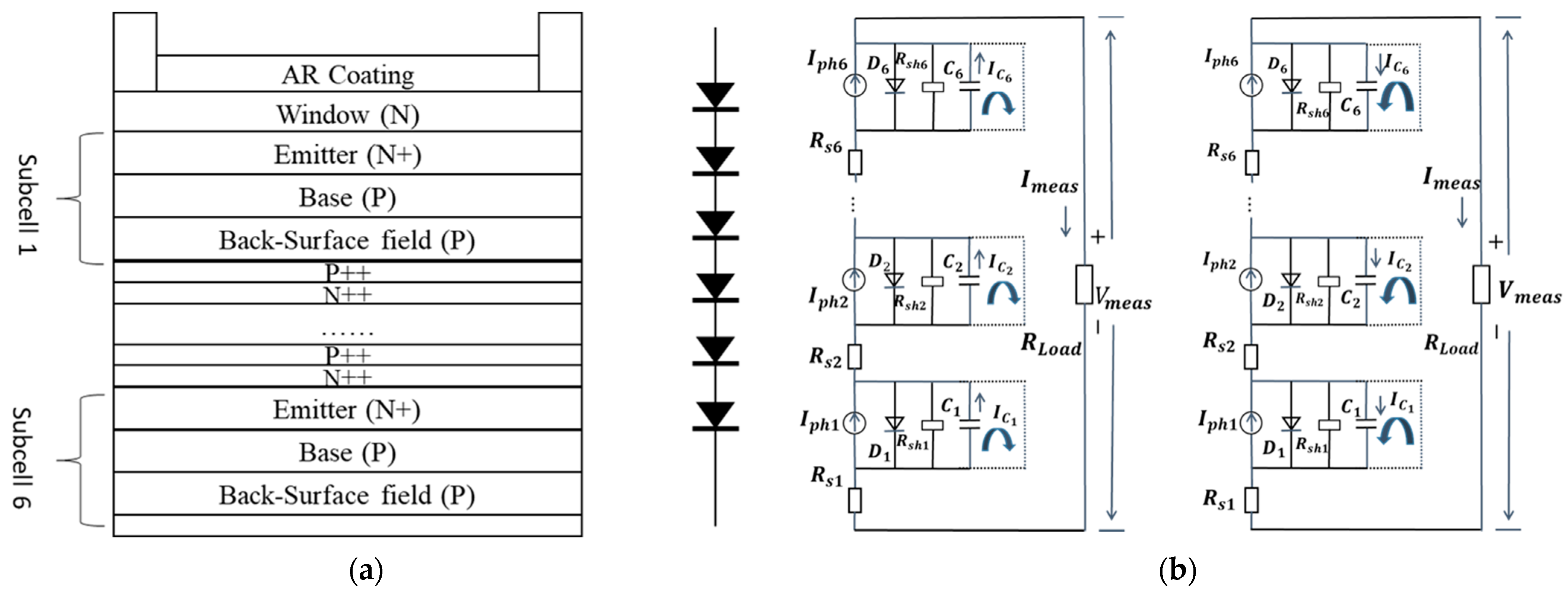
The core structure for LPC power generation is the PN junction. We used a monochromatic GaAs LPC containing six diode models, as shown in Figure 2a. To research the output characteristics of an LPC, the PN junction must be analyzed. The charge in the space charge region of the PN junction is immobile, while the carriers in the neutral region of the PN junction move freely. The difference in conductivity between the space charge region and the neutral region of the PN junction can be equivalent to the capacitance. According to the change in the majority carrier concentration in the space charge region and the change in the minority carrier concentration in the neutral region, the equivalent capacitance can be divided into the barrier capacitance and the diffusion capacitance. The PN junction used to obtain the I–V curves in this paper was always forward biased, and the barrier capacitance was relatively small. The influence of the barrier capacitance was negligible; therefore, the focus was on diffusion capacitance.
The diffusion capacitance of a PN junction refers to the capacitance caused by the charge storage of nonequilibrium minority carriers in the neutral region on both sides of the PN junction. The accumulation and release process of minority carriers in the neutral region is the same as that of capacitor charging and discharging, which corresponds to the diffusion capacitance. When a forward voltage is applied, the distribution of the balanced minority carriers in the neutral region of the PN junction changes. The current generated by the movement of the free carriers directly affects the test results. With the movement of the free carriers, the magnitude and direction of change occur. Electrons in region P are attracted to the positive electrode of the power supply, moving through the external circuit to region N to complete capacitor charging. The direction of the equivalent capacitor charging current is opposite to the direction of the current flowing through the load. After the equivalent capacitor is charged, the excess electrons in region N move through the external circuit to region P, and the direction in this case is the same as that of the current flowing through the load. The circuit model of the GaAs LPC that was used for the test is shown in Figure 2b. The influence of capacitance effect on the test current ( I m e a s ) can be seen directly through the equivalent circuit model. The direction of the capacitive current ( I c ) is the same as I m e a s when the equivalent capacitor is discharged, whereas the directions of I c and I m e a s are different when the equivalent capacitor is charged.

2.3. Optimization of the Acquisition System

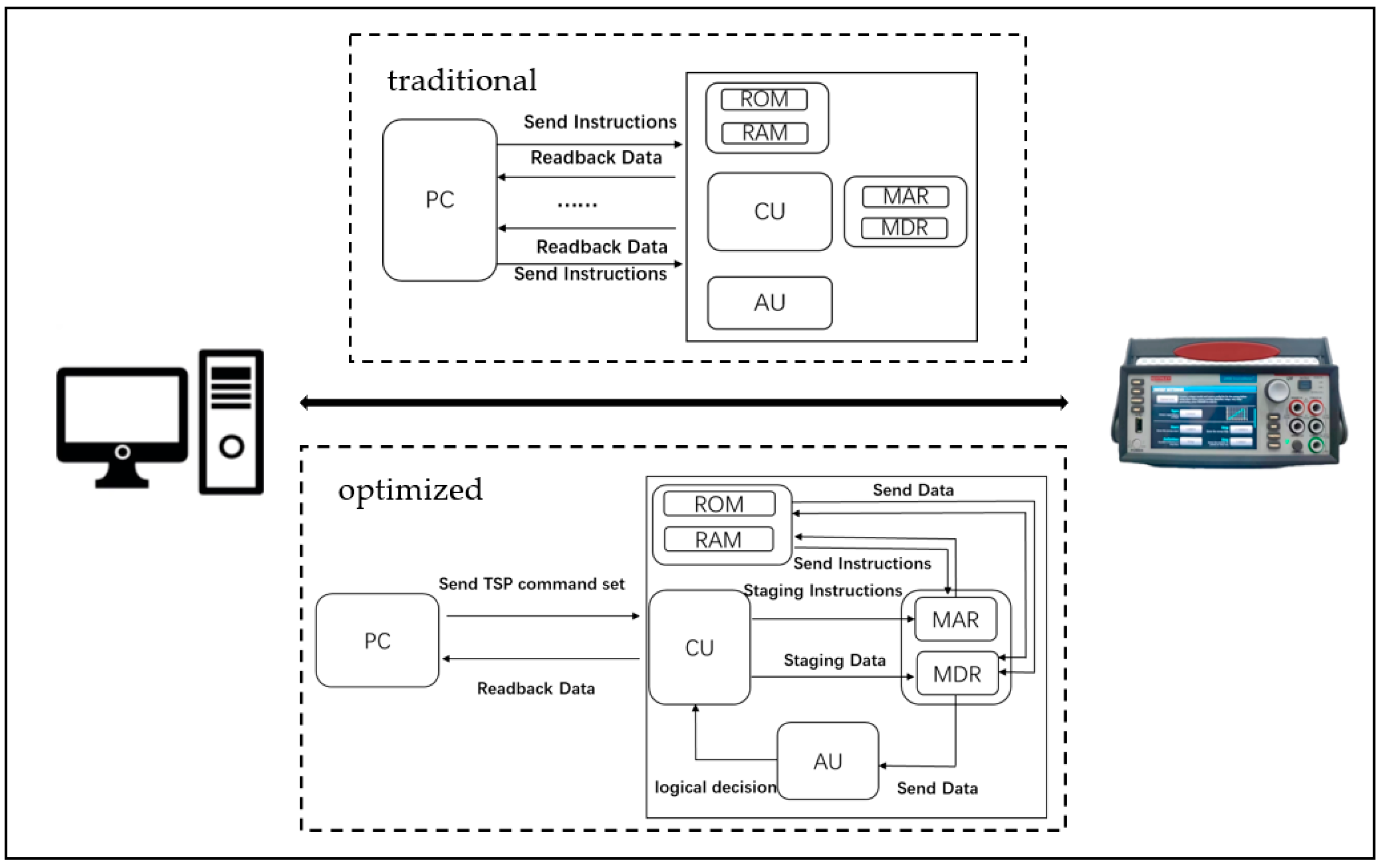
The upper computer acquisition system can quickly obtain all types of index information and output characteristics of the device under test (DUT), which is convenient for further analysis of the DUT. However, the upper computer remotely controls the measuring device to transmit various instructions to the test device through the data bus. The data collected by the measuring device are transmitted to the upper computer by the data bus. The process increases the communication overhead. Measurements obtained in cases with a long laser exposure can suffer from errors induced by the radiation heating of the specimen.
The traditional data acquisition process requires a PC to send various instructions to the test equipment to complete the corresponding operations. In addition, the upper computer executes the algorithm and makes logical data acquisition judgements. After receiving the data, the upper computer makes logical judgments to decide which operation to carry out next and resends instructions to the test equipment. We optimized the test system to address this data acquisition shortcoming. A test script language (TSL) based on the standard programming language Lua was introduced into the test system. Using internal test script processor (TSP) technology, the whole TSL control program can be loaded into the measuring equipment, and the host computer can execute the whole program by sending one instruction, which greatly reduces the number of times that the upper computer needs to pass the data bus to the measuring equipment. Compared with the traditional data communication mode, TSP technology allows algorithms and logic judgments executed in the upper computer to be realized autonomously within the instrument. The data collection diagram is shown in Figure 3.

3. Results

3.1. Test System and Optimized Algorithm

Due to the capacitance characteristics of the PN junction and the influence of temperature, a rapid data acquisition system that obtains the I–V curve of the LPC based on Keithley source measure units (SMUs) was designed and implemented. The upper computer was programmed to control the laser emission and shutdown, and to simultaneously control the SMUs (Keithley 2450, Keithley 2651A, Keithley 4200-SCS) are made by Tektronix in Beaverton City United States to quickly scan the LPC within a short time.
In addition to system construction, the selection of SMU measurement parameters also has an impact on the collected data [19,20]. The measurement parameters of different materials or different structures of the same material are different. Based on the optimized system design, a method for automatically configuring suitable measurement parameters was implemented, as shown in Figure 4. t 1 is associated with the configuration parameter source delay in the device, which is the waiting time before the bias voltage change. t 2 is associated with the configuration parameter NPLC of the device, which is a part of the time of voltage rise or fall. t 3 is associated with the configuration parameter measure delay of the device, which is the time of voltage holding after the bias voltage change and before the measurement. t 4 is associated with the configuration parameter display digits in the device, which determines the time required to write the data into the memory. t 5 is associated with the configuration parameter point in the device, which determines the time it takes for the analog signal to be converted into a digital signal. ε r e a l is the actual hysteresis index, which reflects the effect of the capacitive characteristics of the LPC. ε r e f is the hysteresis index of the reference. D r e a l is the difference between ε r e f and ε r e a l .

3.2. Experiment

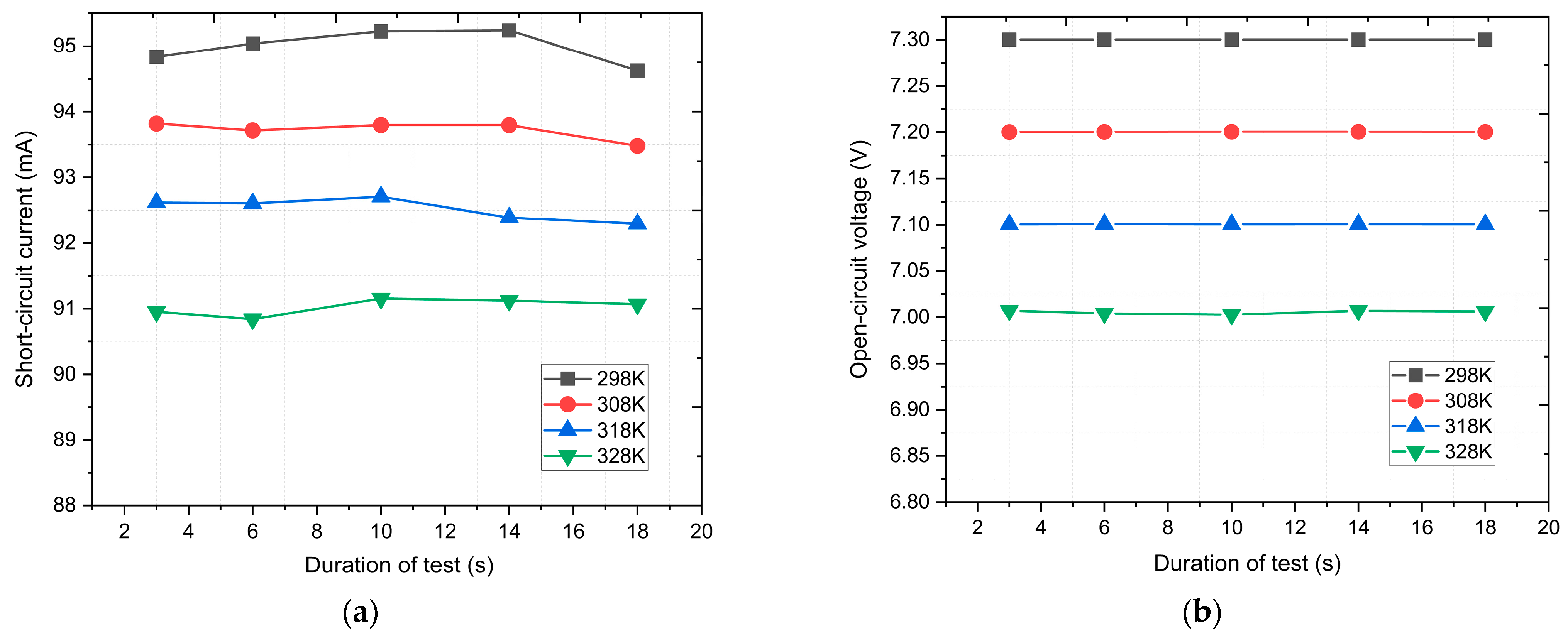
Based on the established test system and optimized test method, we conducted the following experiments to determine the appropriate test time. The influence of the output characteristics of the LPC when the experimental temperature was increased from 298 K to 328 K and test time from 3 s to 18 s was observed first. Significantly, the thermoelectric cooler (TEC) was added to control the temperature of the LPC chip. The short-circuit current ( I s c ) and open-circuit voltage ( V o c ) of the LPC were measured at different temperatures and for different test times, and the results are shown in Figure 5a,b.
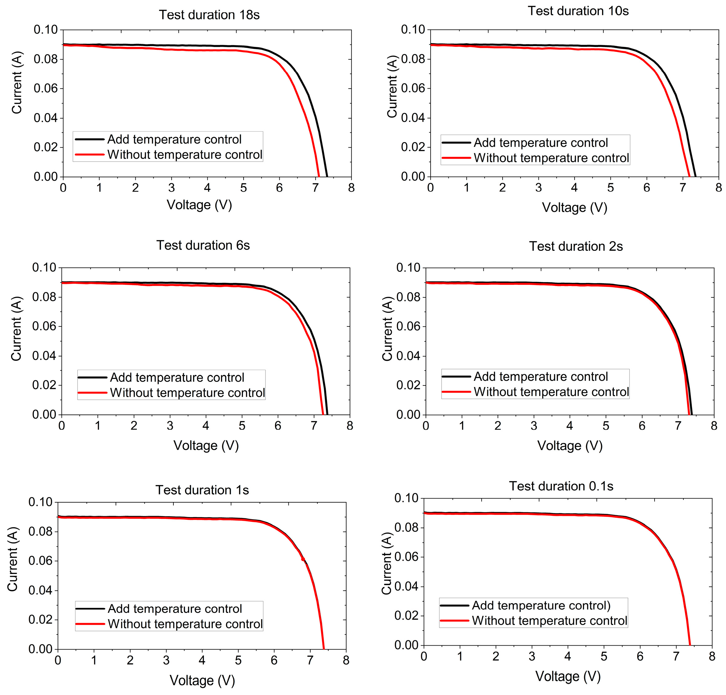
Based on the above experiment, increasing the test time had little effect on Isc and Voc when the temperature was constant. The output characteristics of the same LPC changed at different temperatures under the same test environment. Two conclusions can be drawn: the real influence on the experimental results was caused by the LPC chip heating due to the long test time, and the temperature factor determined the upper limit of the optimal test time. Therefore, another group of comparative experiments was designed to determine the upper time limit that is not affected by temperature. One experiment included the temperature control, and the other experiment did not. When the two groups of experimental data were almost consistent, the influence of the temperature rise over the test time was negligible. The I–V curve measured with and without temperature control remained accurate during the test, as shown in Figure 6.
As the test time increased, the I–V curves with and without TEC showed obvious differences for the same voltage drop, and the photocurrent with TEC was larger than without TEC, as shown in Figure 6. The energy gaps of the semiconductors were due to electron–phonon interactions and thermal dilation. The energy gaps decreased with increasing temperature in GaAs [21]. The barrier height of the PN junction was reduced, and carriers could pass through the PN junction under a relatively small potential. The I–V curve measured without temperature control coincided with the curve under temperature control when the test time was 1 s. In this case, the test data were not affected by the temperature when the test time was less than 1 s. In Figure 6, the test duration of 0.1 is shown as a demonstrative example to illustrate the IV curves (measurements of test durations from 0.1 s to 1 s were omitted for better readability of the chart).
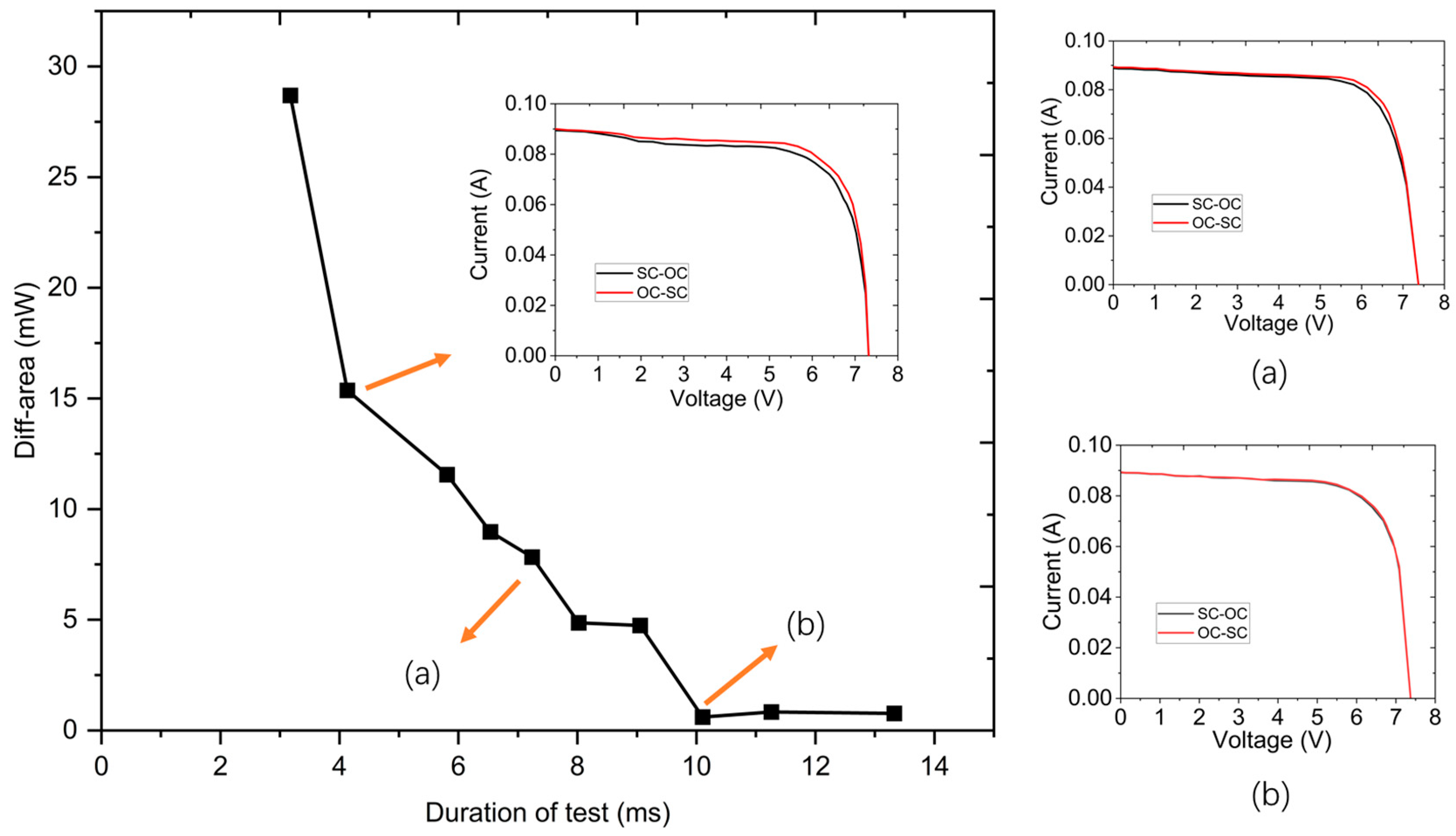
Based on the established rapid test system, the effect of equivalent capacitance on the test was further explored. The forward and reverse scanning of LPC was completed within a short time. When the two groups of scanning data were closer, the I–V curves of the two groups were closer, and the influence of the equivalent capacitance of the LPC was lessened. The experiment was designed and arranged to measure the forward and reverse scanning voltages within a short period of 3 ms~13 ms. We observed the difference between the two curves at different times. The area surrounded by the curves and coordinate axes allowed us to visually compare the differences between the two curves. The area denoted by A is enclosed by a forward scanning curve and coordinate axes. The area denoted by B is enclosed by a reverse scanning curve and coordinate axes. The I–V curve difference in the forward and reverse scanning directions is represented by diff-area, which is the difference between areas A and B. The variation in the relationship between the diff-area and test time t is shown in Figure 7.
As shown in Figure 7, the reverse scan current was larger than the forward scan current under the same applied voltage. This was due to the voltage gradually increasing during the forward scan and equivalent capacitor charge. The direction of Ic was opposite to the direction of the measured current ( I m e a s ), so I m e a s was less than the actual current in this case. The voltage gradually decreased when the SMU reverse scanned the LPC chip, and the equivalent capacitor discharged. The direction of Ic was the same as the direction of I m e a s . Therefore, I m e a s was higher than the actual value, which led to the phenomenon obtained in the experiment above. The diff-area gradually decreased with increasing time t before leveling off. The diff-area was reduced to close to 0 when the test time was increased to 10 ms or higher.
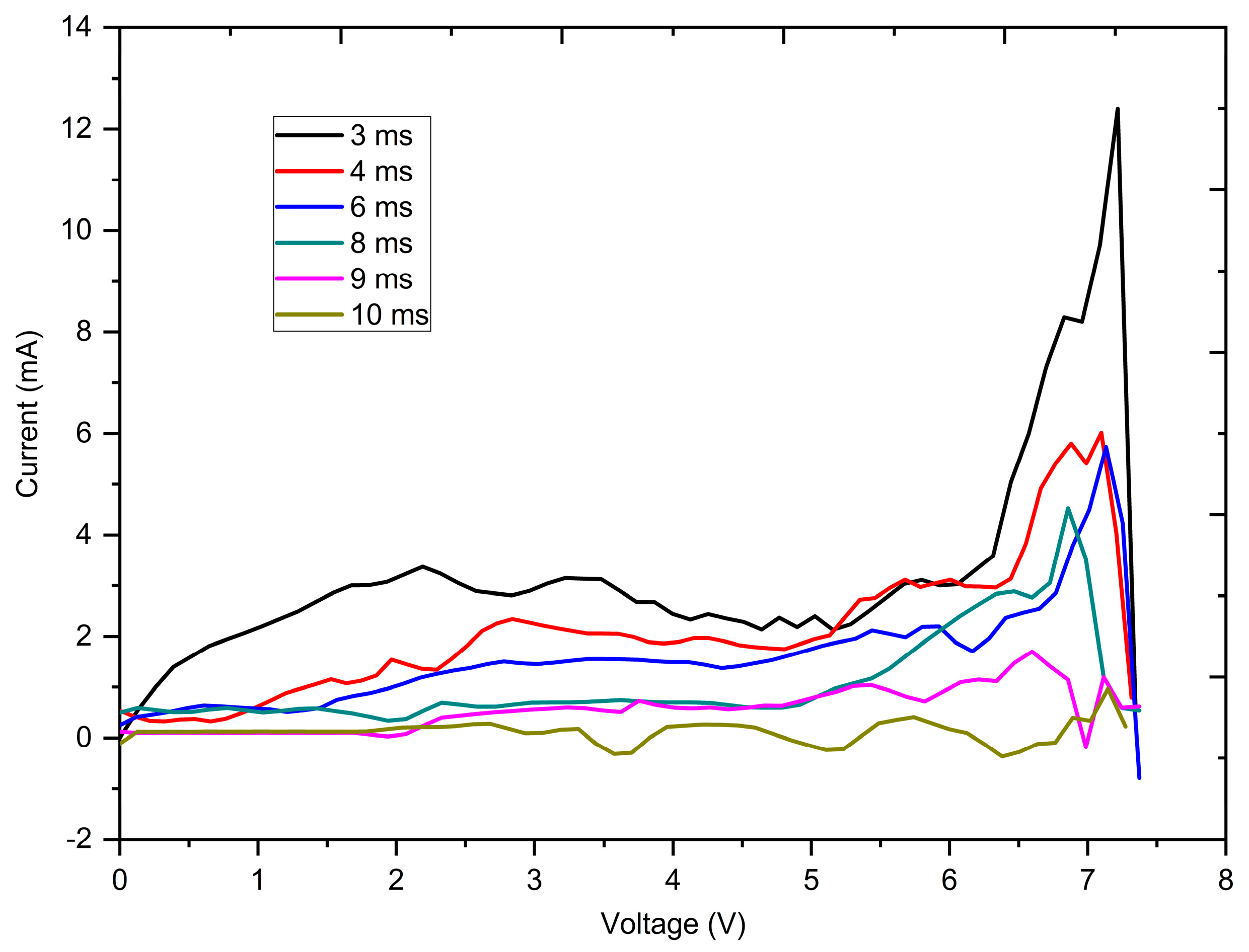
In addition, an interpolation method was introduced to process the data. The principle of interpolation involves subdividing the original curve and inserting values in between. This approach makes the points denser and the curve smoother in the process of data visualization. By obtaining more data points, we can derive a more accurate mathematical model. In our work, we assumed that V 1 and I 1 represent the voltage and current in the forward scan and V 2 and I 2 represent the voltage and current in the reverse scan. When processing the original data, the values of V 1 and V 2 were similar but not equal. Directly subtracting I 1 from I 2 would yield meaningless results. The interpolation method was used to fit the two new curves. By calculating the difference between the two new curves, we obtained the results shown in Figure 8.
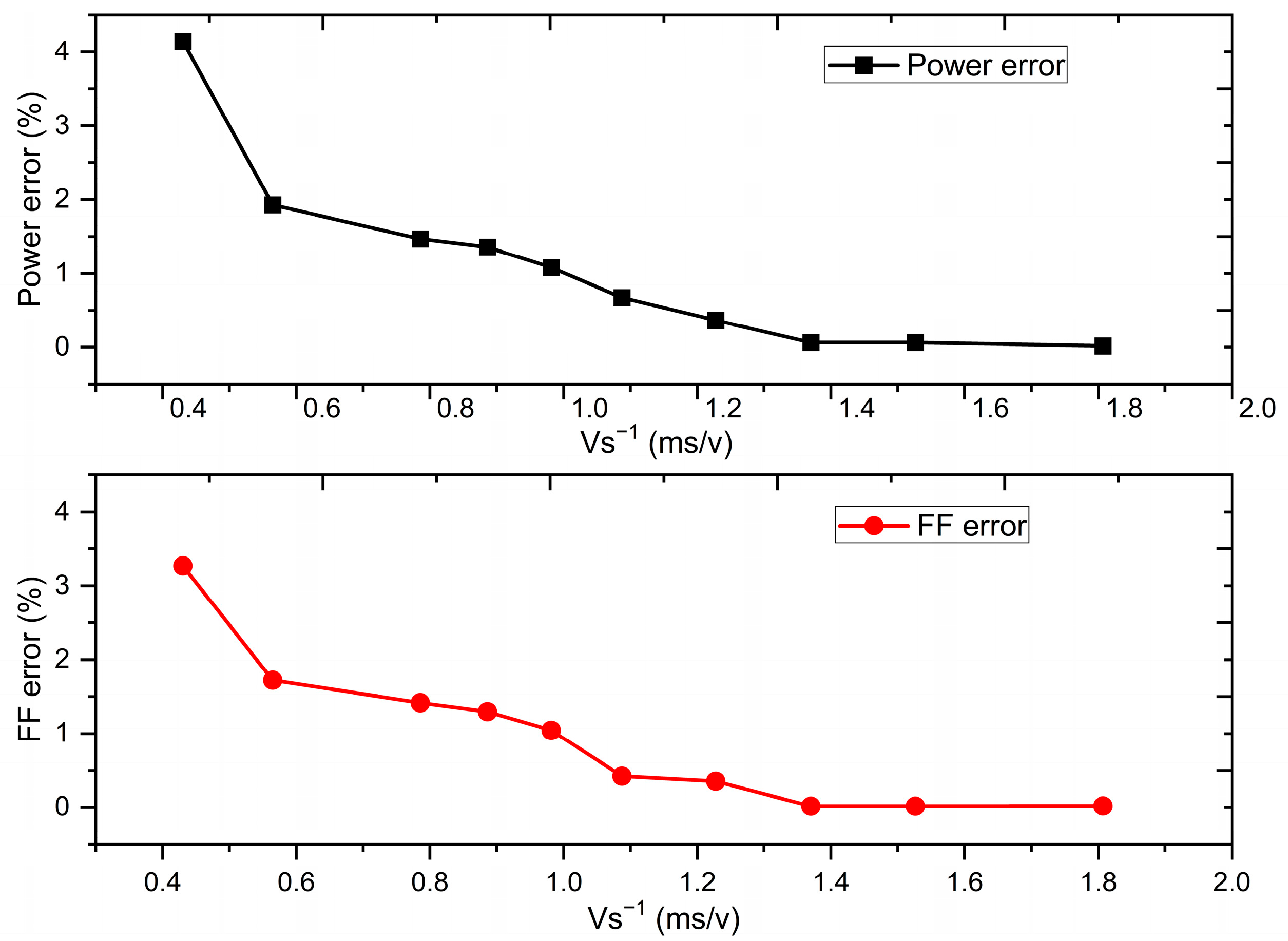
Figure 8 shows that the test time was shorter and the degree to which the curve fluctuated was stronger. As the test time increased, the curve gradually tended to level off. When the test time was 10.103 ms, the curve maintained a small fluctuation around zero. According to Figure 7 and Figure 8, the I–V curves exhibited differences under different scanning directions, and these differences changed over time. It was also observed that the output characteristics of the LPC had some numerical errors. The errors in pmax and the fill factor (FF) between the forward and reverse scanning are denoted by ε p m a x and ε F F :
ε p m a x = p m a x r p m a x f p m a x r + p m a x f   ×   100 %
ε F F = F F r F F f F F r + F F f   ×   100 %
Figure 9 clearly demonstrates the relationship between achieving lower ε p m a x and ε F F while maintaining a lower test speed. When the test speed was faster, the value of hysteresis errors ε p m a x and ε F F were larger. With decreasing test speed and increasing test time, the errors gradually decreased and tended to stabilize. The pmax and FF of the LPC in different scanning directions were almost the same when the test time was approximately 10 ms ( V S 1 is approximately 1.4 ms/v).

4. Discussion

Evaluating the performance of LPCs is particularly important. However, an inappropriate I–V scan time can introduce a significant error into the I–V measurements. In addition to the error resulting from temperature rise due to a longer test time, the transient effect of LPCs also contributed to the deviation. For the multijunction LPC, the impact of equivalent capacitance was even greater. This was because the multijunction LPCs had high-efficiency capabilities and higher open circuit voltages; therefore, more time was needed to reach the individual equilibrium condition. The charge distribution in the LPC was drastically changed when the external power applied fast voltage changes to the LPC. Therefore, the capacitive characteristics of multijunction GaAs LPCs should be considered. In this paper, we successfully built a fast upper computer test system (shown in Section 2.3) to further study the effect of equivalent capacitance. The system combined the powerful data processing ability of the upper computer and the accurate data acquisition capacity of professional measuring equipment. In addition, the collected data was processed directly by the upper computer, which greatly facilitated our further analysis of the LPC. The method was applied to experiments to determine the optimal scanning time for GaAs LPCs, which can also be used for LPCs of other materials.

5. Conclusions

In this paper, we employed TSP technology to build a test system, which was proven to be very effective and convenient. An algorithm for automatically configuring suitable measurement parameters was introduced. This proposed algorithm can be applied to LPCs of different materials. In addition, a series of experiments were carried out based on the constructed system and optimized algorithm. We studied the influence of temperature on GaAs LPC during I–V curve measurements. This study demonstrated that temperature had almost no effect on I–V curve measurements when the test duration lasted up to 1 s. Furthermore, the effect of equivalent capacitance on the measurements was analyzed. It was confirmed in this study that the test time was shorter and the effect of the equivalent capacitance was greater. This work presented the diff-area, reflecting capacitive characteristics that were reduced to almost 0 when the test time was increased to 10 ms or higher. These experiments also obtained a curve using an interpolation method, which maintained a small fluctuation close to 0. Meanwhile, the pmax and FF tended to stabilize at approximately 10 ms. In conclusion, we determined the optimal I–V curve scan time from approximately 10 ms to nearly 1 s of the GaAs LPC.

Author Contributions

Conceptualization, Y.Z. (Yihao Zhang) and C.G.; methodology, Y.Z. (Yihao Zhang) and C.G.; software, Y.Z. (Yihao Zhang); validation, Y.Z. (Yihao Zhang) and Y.Z. (Yikai Zhou); investigation, Y.Z. (Yihao Zhang), R.Z. and W.C.; resources, C.G. and Y.Y.; data curation, Y.Z. (Yihao Zhang); writing—original draft preparation, Y.Z. (Yihao Zhang); writing—review and editing, Y.Y.; supervision, C.G. and Y.Y.; funding acquisition, Y.Y. All authors have read and agreed to the published version of the manuscript.

Funding

This research was funded by the International Science and Technology Cooperation Key Research and Development Program of Science and Technology Agency in Hubei Province (No. 2021EHB018), Project of Outstanding Young and Middle-aged Scientific Innovation Team of Colleges and Universities in Hubei Province (No. T201907), and Overseas Expertise Introduction Center for Discipline Innovation (111 Center).

Institutional Review Board Statement

Not applicable.

Informed Consent Statement

Not applicable.

Data Availability Statement

Not applicable.

Conflicts of Interest

The authors declare no conflict of interest.

References

  1. Wojtczuk, S.J. Long-wavelength laser power converters for optical fibers. In Proceedings of the 26th IEEE Photovoltaic Specialists, Anaheim, CA, USA, 29 September–3 October 1997. [Google Scholar] [CrossRef]
  2. Zhao, Y.; Li, S.; Ren, H.; Li, S.; Han, P. Energy band adjustment of 808 nm GaAs laser power converters via gradient doping. J. Semicond. 2021, 42, 032701. [Google Scholar] [CrossRef]
  3. Fafard, S. High-Efficiency and High-Power Multijunction InGaAs/InP Photovoltaic Laser Power Converters for 1470 nm Photonics. Photonics 2022, 9, 438. [Google Scholar] [CrossRef]
  4. Zhao, Y.; Liang, P.; Ren, H.; Han, P. Enhanced efficiency in 808 nm GaAs laser power converters via gradient doping. AIP Adv. 2009, 9, 105206. [Google Scholar] [CrossRef] [Green Version]
  5. Oliva, E.; Dimroth, F. GaAs converters for high power densities of laser illumination. Prog. Photovolt. 2008, 16, 289–295. [Google Scholar] [CrossRef]
  6. Olsen, L.C.; Huber, D.A. High efficiency monochromatic GaAs solar cells. In Proceedings of the 22th IEEE Photovoltaic Specialists, Las Vegas, NV, USA, 7–11 October 1991. [Google Scholar] [CrossRef]
  7. Nandon, S. InAlGaAs/InP-Based laser photovoltaic converter at 1070 nm. IEEE Electron Device Lett. 2016, 37, 1154–1157. [Google Scholar] [CrossRef]
  8. Shan, T.; Qi, X. Design and optimization of GaAs photovoltaic converter for laser power beaming. Infrared Phys. Technol. 2015, 71, 144–150. [Google Scholar] [CrossRef]
  9. Reichmuth, S.K. On the temperature dependence of dual-junction laser power converters. Prog. Photovolt. Res. Appl. 2017, 25, 67–75. [Google Scholar] [CrossRef] [Green Version]
  10. Walker, A.W. Optimal laser wavelength for efficient laser power converter operation over temperature. Appl. Phys. Lett. 2016, 108, 241104. [Google Scholar] [CrossRef]
  11. Mau, S.; Krametz-Proc, T. Influence of solar cell capacitance on the measurement of I-V-curves of PV-modules. In Proceedings of the 20th European Photovoltaic Solar Energy Conference, Barcelona, Spain, 6–10 June 2005. [Google Scholar]
  12. Sinton, R.A. A solution to the problem of accurate flash-testing of high-efficiency modules. In Proceedings of the 21th European Photovoltaic Solar Energy Conference, Munchen, Germany, 4–8 September 2006. [Google Scholar]
  13. Friesen, F.; Ossenbrink, H.A. Capacitance effects in high-efficiency cell. Sol. Energy Mater Sol. Cells 1997, 48, 77–83. [Google Scholar] [CrossRef]
  14. Granek, F. Advanced system for calibration and characterization of solar cells. Opto-Electron. Rev. 2004, 12, 57–67. [Google Scholar]
  15. Roth, T.; Wichmann, D. In-depth analysis of transient errors of inline IV measurements. Energy Procedia 2011, 8, 82–87. [Google Scholar] [CrossRef] [Green Version]
  16. Edler, A.; Schlemmer, M. Understanding and overcoming the influence of capacitance effects on the measurement of high efficiency silicon solar cells. Energy Procedia 2012, 27, 267–272. [Google Scholar] [CrossRef] [Green Version]
  17. Kojima, H.; Iwamoto, K. Accurate and rapid measurement of high-capacitance PV cells and modules using a single short pulse light. In Proceedings of the 2014 IEEE 40th Photovoltaic Specialist Conference, Denver, CO, USA, 8–13 June 2014. [Google Scholar]
  18. Herman, M. Optimal I-V curve scan time of solar cells and modules in light of irradiance level. Int. J. Photoenergy 2012, 2012, 151452. [Google Scholar] [CrossRef] [Green Version]
  19. Gao, Q.; Zhang, Y. Effects of I-V measurement parameters on the hysteresis effect and optimization in high-capacitance PV module testing. IEEE J. Photovolt. 2018, 8, 710–718. [Google Scholar] [CrossRef]
  20. Moreno-Romero, P.M. Voltage scanning speed determination and current voltage curves of different types of perovskite solar cells. IEEE J. Photovolt. 2022, 12, 611–617. [Google Scholar] [CrossRef]
  21. Gopalan, S.; Lautenschlager, P. Temperature dependence of the shifts and broadenings of the critical points in GaAs. Phys. Rev. B 1987, 35, 5578–5584. [Google Scholar] [CrossRef] [PubMed]
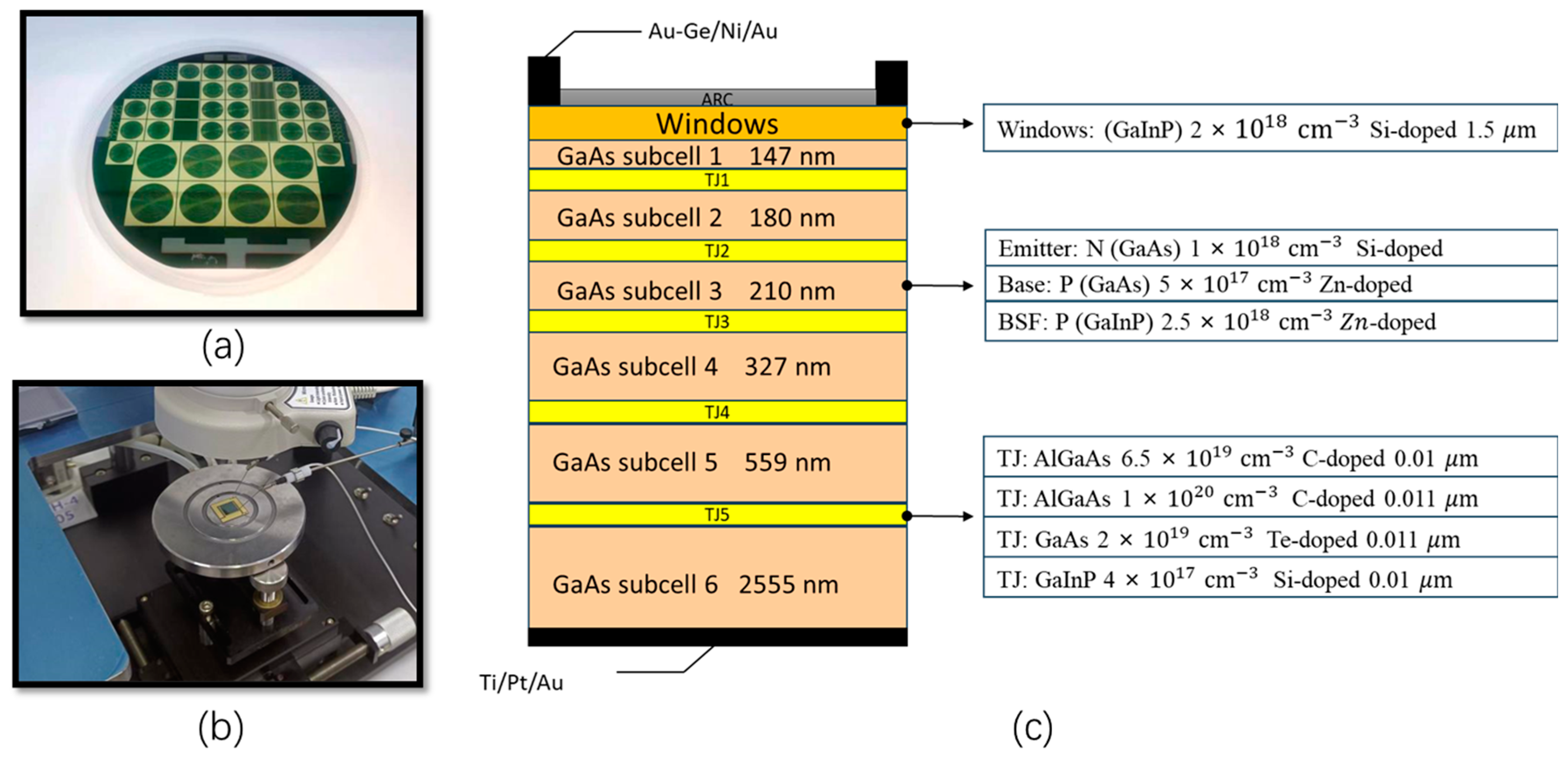
Figure 1. Schematics of the multijunction GaAs LPC that was used for testing. (a) LPC wafer, (b) LPC chips in the platform, (c) structures of the multijunction GaAs LPC.
Photonics 10 00762 g001
Figure 2. (a) Schematics of the test LPC containing six diode models. (b) The equivalent model of a multi-junction LPC circuit when the equivalent capacitance is charged and discharged.
Photonics 10 00762 g002
Figure 3. Schematics comparing the traditional data acquisition system with the optimized data acquisition system.
Photonics 10 00762 g003
Figure 4. Schematic of the data acquisition and automatic parameter configuration process.
Photonics 10 00762 g004
Figure 5. The influence of the output characteristics of the LPC: (a) short-circuit current; (b) open-circuit voltage.
Photonics 10 00762 g005
Figure 6. Comparison of test results with and without temperature control at different test times.
Photonics 10 00762 g006
Figure 7. Schematics of variation of diff-area over test time. (a) the result of the test duration of 6.535 ms, (b) the result of the test duration of 10.103 ms.
Photonics 10 00762 g007
Figure 8. Time dependent relationship diagram of the current difference between forward and reverse scans.
Photonics 10 00762 g008
Figure 9. Schematics of the hysteresis errors ε p m a x and ε F F vs. scanning speed.
Photonics 10 00762 g009
Disclaimer/Publisher’s Note: The statements, opinions and data contained in all publications are solely those of the individual author(s) and contributor(s) and not of MDPI and/or the editor(s). MDPI and/or the editor(s) disclaim responsibility for any injury to people or property resulting from any ideas, methods, instructions or products referred to in the content.