Article

Racetrack Ring Resonator Integrated with Multimode Interferometer Structure Based on Low-Cost Silica–Titania Platform for Refractive Index Sensing Application

by
Muhammad A. Butt
*,
Muhammad Shahbaz
and
Ryszard Piramidowicz
Institute of Microelectronics and Optoelectronics, Warsaw University of Technology, Koszykowa 75, 00-662 Warszawa, Poland
*
Author to whom correspondence should be addressed.
Photonics 2023, 10(9), 978; https://doi.org/10.3390/photonics10090978
Submission received: 11 August 2023 / Revised: 22 August 2023 / Accepted: 25 August 2023 / Published: 27 August 2023

Abstract

:
In this work, a racetrack ring resonator (RTRR) integrated with a multimode interferometer (MMI) structure based on a silica–titania (SiO2:TiO2) platform is projected for refractive index sensing application. The typical ring resonator structure requires a gap of ~100 nm to 200 nm between the bus waveguide (WG) and the ring structure which makes it challenging to fabricate a precise device. Thus, the device proposed in this paper can be considered a “gapless” ring resonator structure in which the coupling of light between the ring and bus WG can be achieved via an MMI coupler. A minor change in the refractive index in the vicinity of the MMI structure can trigger a shift in the resonance wavelength of the device. Thus, this simple and fascinating structure can be employed as a refractive index sensor. The device’s sensitivity is ~142.5 nm/RIU in the refractive index range of 1.33 to 1.36 with a figure of merit (FOM) of 78.3. This simple device structure can potentially be fabricated via a low-cost and highly efficient sol–gel process and dip-coating method combined with the nanoimprint lithography (NIL) method.

1. Introduction

Multi-mode interference (MMI) structure is based on the ‘Talbot effect,’ discovered in 1886 by Henry Fox Talbot [1]. It involves self-imaging of injected optical fields in multi-mode WGs, aiding the expansion of compact and efficient photonic devices and components. The fundamental building block of an MMI device is a multimode waveguide (WG) capable of supporting several modes of light propagation. When light travels through this WG, the different guided modes interfere with each other. This interference phenomenon leads to the reconstitution of the input optical field in one or more images at regular intervals along the direction of propagation, depending on the length and width of the WG. This remarkable effect is commonly described as the “self-imaging principle” [2].
Since its initiation in 1975, MMI couplers have seen an instant development [3]. They are generally used in various Planar Lightwave Circuit (PLC) applications, including power splitters, optical switches, and wavelength division multiplexers/demultiplexers. MMI couplers based on different materials, such as LiNBO3 [4], SOI [5], InP [6], polymer [7], silica-on-silicon (SOS) [8], etc., have been reported. The versatility and efficiency of MMI couplers make them a crucial component in modern integrated photonics devices. The self-imaging principle, based on high-index-contrast WGs, is used to develop MMI devices typically accomplished with InGaAsP/InP [9] and GaAs/AlGaAs [10], but researchers have reported work on low-index-contrast optical WG MMI devices, particularly those based on silica-on-silicon (SOS) WGs [11,12].
Over the past twenty years, there has been a substantial transformation in the field of optical sensors, predominantly driven by advancements in optical device manufacturing and the widespread adoption of various sensing applications [13,14,15,16,17]. This period has seen a revolution, leading to incredible progress in both the development and utilization of photonic sensors based on resonant WG gratings [18], surface plasmon resonance [19,20,21], and guided-mode resonance [22,23]. Researchers have been actively exploring the applications of MMI structures in WG sensor technology [24,25]. These studies have focused on inspecting the potential uses and benefits of MMI devices for sensing purposes. A team of researchers presented a novel approach to microring resonators (MRR) using 4 × 4 MMI couplers for highly sensitive multichannel chemical and biological sensing [26]. The compact design exhibited superior sensitivity compared to existing structures. They optimized and demonstrated the sensor using silicon WGs through numerical simulations and the transfer matrix method (TMM). The sensor successfully detected glucose and ethanol concentrations simultaneously, achieving high sensitivity (9000 nm/RIU) and low detection limits (2 × 10⁻⁴ for glucose and 1.3 × 10⁻⁵ for ethanol) [26].
In a different study [27], researchers fabricated an MRR incorporating a multimode interference coupler on a polymer platform using a UV-based soft nanoimprint technique. The fabrication process involved the use of a special type of fluorinated polymer known as perfluoropolyether (PFPE) for creating a flexible soft mold. Through careful optimization of the proportions between Ormocore and the thinner maT materials, they successfully produced the MRR with minimal residual layer. The proposed device demonstrated a spectrum with an FSR and ER of ~335 pm and ~11.6 dB, respectively, achieving a high Q factor of 2.3 × 10⁴ [27]. In [28], the researchers put forward and designed an innovative S-bend resonator as a RI sensor, utilizing a multi-mode WG. The S-bend resonator was composed of a ridge WG, an MMI coupler, and multiple bend structures. The researchers achieved inspiring results, with a Q-factor of 2.3 × 10³ and a sensitivity of ~52 nm/RIU [28].
Ring resonators (RRs) are integrated photonic devices employed to sense changes in the environment, such as variations in refractive index, temperature, pressure, or biological interactions [29,30]. They are established on the principle of optical resonance and are commonly used in a variety of applications due to their numerous advantages and magnitudes. RR sensors offer high sensitivity to small changes in the surrounding environment. When the refractive index of the material around the ring changes, it triggers a shift in the resonant wavelength, which can be accurately determined. This sensitivity is particularly helpful in applications like chemical and biological sensing [13]. In [31], we exhibited a standard RR structure based on the SiO2:TiO2 platform for refractive index sensing applications. The gap between the bus WG and the ring is around 100 nm which is quite challenging to attain by employing a standard lithography process.
In this work, we proposed a novel design of a racetrack ring resonator (RTRR) integrated with an MMI structure based on a low-cost silica–titania (SiO2:TiO2) optical platform for refractive index sensing applications. The device design is straightforward and does not need a gap between the bus WG and a ring for evanescent field coupling. Hence, we assume that it can be effectively fabricated via a cost-effective nanoimprint lithography (NIL) method as declared in our previous study [32]. The sol–gel process allows us to manufacture a wide range of materials, including glasses, ceramics, and composites [33]. It offers versatility in tailoring the properties of the final product by varying the precursor materials and process parameters. The sol–gel process can produce thin films with precise control over thickness and composition, making them functional for applications like anti-reflective coatings, protective layers, and optical devices [32,33,34,35].
The dip-coating method is reasonably simple and cost-effective compared to other thin-film deposition techniques [36]. It does not demand complex equipment or elaborate setups [37]. Dip-coating can produce uniform and consistent thin films over large or complex-shaped substrates, ensuring even coverage and thickness distribution [38]. The dip-coating process is greatly reproducible, allowing for consistent results when performed under the same conditions [39]. In our previous work [35], high-quality SiO2:TiO2 thin films are deposited on BK7 glass via a sol–gel process and a dip-coating method. Thus, we assume that the proposed sensing device in this paper can be effectively fabricated by employing the NIL method as justified in our previous work [32].

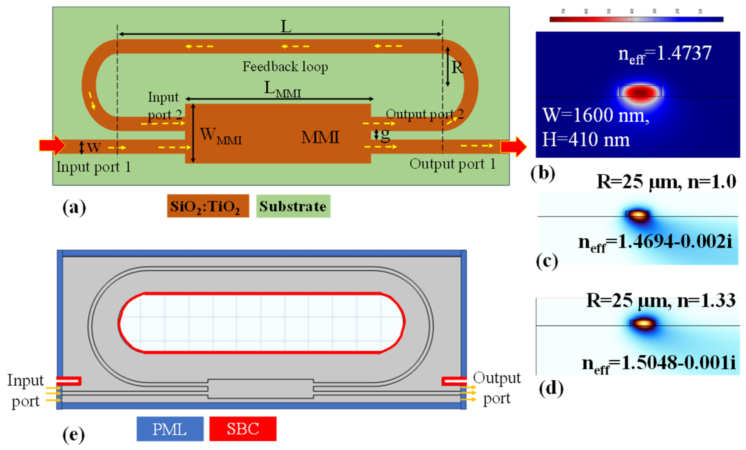
2. Device Design and Parametric Optimization

The graphical illustration of the RTRR integrated with the MMI structure is exhibited in Figure 1a. The device contains two input and two output ports connected to the MMI segment. The output port 2 is further combined with an RTRR structure which has a radius R and acts as a feedback loop. The width (W) of the input and output WGs are fixed at 1.6 µm which satisfies the single mode condition at the operational wavelength of 1.55 µm. The total height of the device is assumed to be 0.41 µm to support the TE0 mode having an effective refractive index of 1.4737 as shown in Figure 1b. Later, this effective index is employed in designing the device in a 2D numerical model. The width and length of the MMI structure are denoted as WMMI and LMMI, respectively. The WMMI is fixed at 8 µm which specifies a region where multiple modes can interfere. The light is launched at the input port 1 which couples to the RTRR structure via a MMI coupler. The resonance condition is satisfied at specific operational wavelengths which can be collected at output port 1. The feedback loop contains two semi-circular bend WGs; therefore, it is important to plot the E-field distribution and determine the effective refractive index of the mode propagating in the WGs with a bending radius (R) of 25 µm in the presence of ambient refractive index of 1.0 and 1.33 as shown in Figure 1c,d, respectively. The results suggest that WGs with R = 25 µm can support fundamental mode which stabilizes while propagating in the straight WG. Table 1 describes the geometric parameters used to optimize the device design for sensing applications.
The transmission and E-field distributions of the sensing device are verified by the finite element method (FEM) by employing commercially available COMSOL Multiphysics software 6.1. Perfect matching layer (PML) and scattering boundary condition (SBC) are applied to simulate the behavior of EM wave propagating in unbound domains as shown in Figure 1e. The numeric ports are also assigned to the bus WG to excite the input of the bus WG (input port) and collect the transmission at the output (output port). PML is an absorbing boundary condition that allows for the reduction of reflection and surplus wave interactions at the boundaries of the simulation domain. Moreover, meshing is a crucial step in the FEM process, and it plays a significant role in the accuracy and efficiency of simulations in COMSOL Multiphysics. Meshing involves dividing the computational domain into smaller geometric elements, for instance, triangles or tetrahedra in 2D or 3D, respectively. Each element corresponds to a discrete region where the equations of the physics being simulated can be approximated and solved. For our model, we choose “physics-controlled mesh”, which provides an appropriate mesh size to acquire accurate results.
To obtain a 3 dB 2 × 2 MMI coupler, the length of the multimode segment can be calculated as [27]:
L M M I = p L π 2 ;   where   p   =   1 ,   2 ,   3 ,   4
where L π is the beat length of the two lowest-order modes and can be stated as:
L π = π β o β 1 = 4 n e f f W M M I 2 3 λ ;
where neff is the effective refractive index, λ is the free-space wavelength, WMMI is the width of the MMI segment, which is fixed at 8 µm, and βo and β1 are the propagation constants of the fundamental and first-order lateral modes, respectively. From Equation (1), the LMMI is calculated as ~40.56 µm. The precise length of the MMI segment is attained via FEM as shown in Figure 2. The schematic representation of the 2 × 2 MMI segment is shown in Figure 2a which will be integrated with the final device configuration. The TE polarized light at the operational wavelength of 1.55 µm is launched at input port 1 and the transmission (a.u) spectrum obtained at output port 1 and output port 2 is plotted versus LMMI as shown in Figure 2b. The LMMI is varied from 40 µm to 114 µm, whereas W, WMMI, and g are fixed at 1.6 µm, 8 µm, and 2 µm, respectively. The power ratio (P1/P2) of the output ports is plotted in Figure 2c which indicates several points where equal power distribution can be achieved. However, looking at the maximum power transmission of ~0.31 which is obtained at both output ports, LMMI = 44 µm is selected. The normalized E-field distribution in the MMI structure for LMMI = 44 µm (equal power distribution at output ports) and LMMI = 68 µm (unequal power distribution at output ports) is presented in Figure 2d,e, respectively.
The transmission spectrum of the RTRR integrated MMI structure is simulated for R = 25, 30, 35, and 40 µm, while keeping the remaining structural variables such as LMMI, WMMI, L, W, and g at 44 µm, 8 µm, 94 µm, 1.6 µm, and 2 µm, respectively. For the spectral range of 1.548 µm to 1.560 µm, almost three resonance dips appear as shown in Figure 3a. The free spectral range (FSR) of a RR is a key parameter that characterizes its optical behavior. The FSR refers to the spacing between adjacent resonant frequencies or wavelengths at which the RR exhibits constructive interference [40]. In other words, it is the frequency difference between two consecutive resonance peaks of the RR’s transmission spectrum [31]. From Figure 3b, it can be seen that the FSR of the device reduces from 4.65 nm to 3.675 nm as R increases from 25 µm to 40 µm. The FSR is a vital parameter in various applications, such as in WDM systems and the design of optical filters and lasers [41,42]. By controlling the FSR, the operating frequencies of the RR can be determined, and tailor its performance to specific applications. The E-field distribution at the resonance wavelength where a sharp dip in the transmission spectrum takes place and the wavelength at which light transmits at output port 1 is shown in Figure 3c,d, respectively.

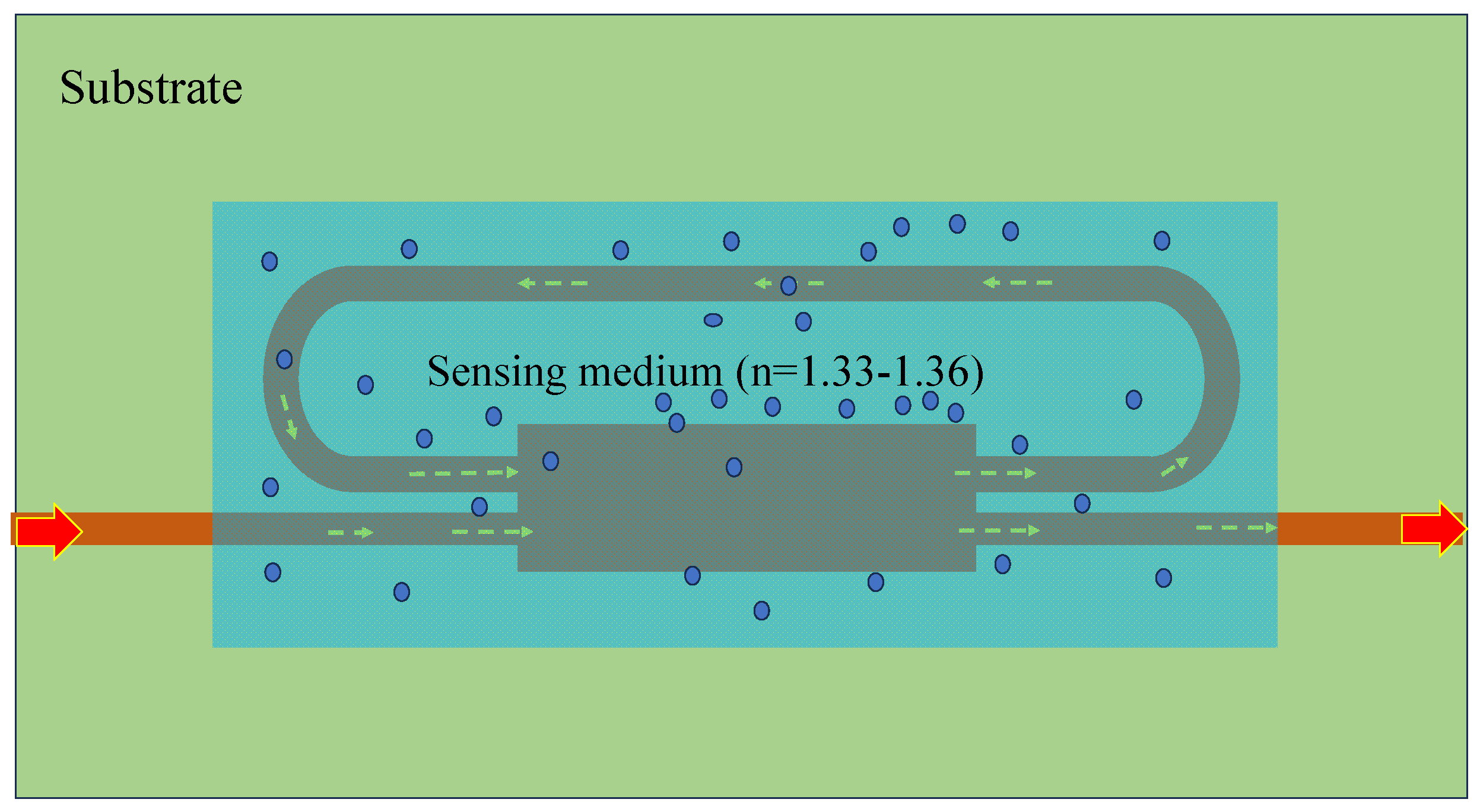
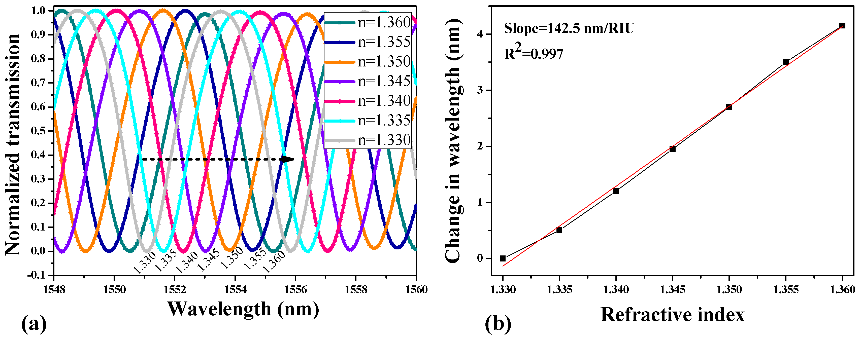
3. Refractive Index Sensing Operation

The basic principle of refractive index sensing operation involves exploiting the interaction of light with the material under investigation. Refractive index sensing devices are used in biosensors to detect biomolecules and analytes or monitor chemical reactions [43]. The refractive index is an essential property in the context of bioanalytes, as it can provide valuable information about their composition and concentration. Bioanalytes refer to various biomolecules, cells, or biological substances that are of interest for analysis in biological and biomedical research. Some common bioanalytes include proteins, nucleic acids (DNA and RNA), peptides, antibodies, antigens, cells, and small molecules like glucose and ions [44]. The refractive index of a bioanalyte depends on its chemical composition, concentration, temperature, and wavelength of light used for measurement. One significant advantage of refractive index sensors in bioanalyte analysis is that they enable label-free detection. This indicates that the analytes do not require any specific labels or tags, reducing the complexity and cost of the analysis [45].
The RTRR-integrated MMI structure is immersed in a sensing medium (see Figure 4), where the change in the refractive index of the medium can influence the interference pattern of the propagating modes in the MMI structure resulting in the shift in the resonance dip. The sensitivity of the photonic sensor is typically quantified in terms of the smallest detectable change in the measured quantity that can be reliably sensed by the device. Highly sensitive photonic sensors authorize precise and accurate measurements of small changes in physical quantities for instance temperature, pressure, strain, displacement, or chemical concentrations [29,30]. This level of precision is crucial in applications where even petite variations can have substantial implications. The sensitivity of the refractive index sensor based on RTRR-integrated MMI structure is evaluated as:
S e n s i t i v i t y   n m R I U = λ r e s n ;
where ∆λres and ∆n are the variation in resonance wavelength and change in the refractive index of the ambient medium, respectively.
The normalized transmission spectrum of the RTRR-integrated MMI structure in the presence of different ambient refractive indices varied between 1.33 and 1.36 with a step size of 0.05 is shown in Figure 5a. The resonance wavelength performs a redshift as the ambient index increases due to a change in the effective refractive index of the modes interfering in the MMI structure. The change in resonance wavelength shift concerning the variation in ambient refractive index is plotted in Figure 5b (black dotted line). A common method for determining the relationship between two variables is to fit a straight line to a collection of data points using linear regression (red line in Figure 5b). One of the most notable results of this method is the slope of the line, which shows how quickly the dependent variable changes for each unit increase in the independent variable. The resonant wavelength versus RIU graph can be fitted linearly to get a slope of about 142.5 nm/RIU. The sensitivity obtained with the RTRR integrated with the MMI structure resembles our previous results on the SiO2:TiO2 platform-based standard RR structure [31]. However, we believe that the proposed structure is much simpler and more flexible in fabrication. The figure of merit (FOM) of the sensing device is expressed in terms of:
F O M = S F W H M
where S is the device’s sensitivity and FWHM is the full width at half maximum of the resonant dip, which is ~1.82 nm, and, correspondingly, the FOM of the device is ~78.3.
In [46], the authors presented a chip-scale photonic system in their study, aimed at detecting gas composition and pressure at room temperature. This system relied on a slotted Si MRR for its operation. In [47], the researchers documented the development of a liquid sensing device that utilized a Ge–Sb–Se MRR operating at a wavelength of 1550 nm. In the study [48], a label-free optical biosensor employing a microring resonator, which utilized lithium niobate-on-insulator (LNOI) technology, was conceptualized and simulated for applications in biosensing. Another study introduced a design guideline for an MZI sensor utilizing SOI nanowires [49]. This guideline enabled the adjustment of sensitivity through the strategic selection of MZI arm lengths, as outlined by the provided data within the research paper. Recently, a unique sensor designed for MIR biochemistry applications was introduced [50]. This sensor employed a configuration featuring two suspended GaAs WGs within an asymmetric MZI setup. The device performance is compared with several other novel designs, as shown in Table 2.

4. Concluding Statements

A multimode interferometer (MMI) is an optical device used in integrated photonics for various applications, including optical communications and sensors. It is based on the principle of interference, where light waves from different modes interact constructively or destructively to produce an output pattern. In this work, a numerical study on RTRR integrated with MMI structure is aimed at refractive index sensing application. The structure is based on a low-cost SiO2:TiO2 material platform where high-quality thin films are obtained via the sol–gel process and a dip-coating method. The sensitivity and FOM of the proposed device are ~142.5 nm/RIU and 78.3, respectively. The cost of the photonic sensor is an important factor, especially for commercial and mass-market applications, as it affects the feasibility of operating the sensor in various scenarios. We consider that this device can be realized via a low-cost NIL method which overall cut down the cost of production of this photonic sensing device.

Author Contributions

Conceptualization, M.A.B. and R.P.; methodology, M.A.B.; software, M.A.B.; validation, M.A.B. and R.P.; formal analysis, M.A.B.; investigation, M.A.B.; resources, R.P.; data curation, M.A.B.; writing—original draft preparation, M.A.B. and M.S.; writing—review and editing, M.A.B., M.S. and R.P.; visualization, M.A.B. and M.S.; supervision, R.P.; project administration, R.P.; funding acquisition, M.A.B. All authors have read and agreed to the published version of the manuscript.

Funding

The research is co-financed by the Foundation for Polish Science from the European Regional Development Fund within the project POIR.04.04.00-00-14D6/18 “Hybrid Sensor Platforms for Integrated Photonic Systems based on Ceramic and Polymer Materials (HYPHa)” (TEAM-NET program).

Institutional Review Board Statement

Not applicable.

Informed Consent Statement

Not applicable.

Data Availability Statement

Not applicable.

Acknowledgments

The author acknowledges the support from the Warsaw University of Technology for the completion of this work.

Conflicts of Interest

The authors declare no conflict of interest.

Abbreviations

Racetrack ring resonator = RTRR; multimode interferometer = MMI; finite element method = FEM; perfect matching layer = PML; scattering boundary condition = SBC; silica–titania = SiO2:TiO2; nanoimprint lithography = NIL; waveguide = WG.

References

  1. Talbot, H. LXXVI. Facts relating to optical science. No. IV. Lond. Edinb. Dublin Philos. Mag. J. Sci. 1836, 9, 401–407. [Google Scholar] [CrossRef]
  2. Bryngdahl, O. Image formation using self-imaging techniques. J. Opt. Soc. Am. 1973, 63, 416–419. [Google Scholar] [CrossRef]
  3. Ulrich, R. Light-propagation and imaging in planar optical waveguides. Nouv. Rev. d’Optique 1975, 6, 253–262. [Google Scholar] [CrossRef]
  4. Li, M.; Rao, L.; He, X.; Tian, F.; Pan, X.; Xin, X. Low-loss, broadband MMI coupler based on thin film lithium niobate platform. Phys. Scr. 2023, 98, 035506. [Google Scholar] [CrossRef]
  5. Tsao, S.-L.; Guo, H.-C.; Chen, Y.-J. Design of a 2 × 2 MMI MZI SOI electro-optic switch covering C band and L band. Microw. Opt. Technol. Lett. 2002, 33, 262–265. [Google Scholar] [CrossRef]
  6. Mu, S.; Liu, K.; Wang, S.; Zhang, C.; Guan, B.; Zou, D. Compact InGaAsP/InP 3 × 3 multimode-interference coupler-based electro-optic switch. Appl. Opt. 2016, 55, 1795–1802. [Google Scholar] [CrossRef] [PubMed]
  7. Al-Hetar, A.M.; Mohammad, A.B.; Supa’At, A.S.M.; Shamsan, Z.A.; Yulianti, I. Fabrication and characterization of polymer thermo-optic switch based on mmi coupler. Opt. Commun. 2011, 284, 1181–1185. [Google Scholar] [CrossRef]
  8. Chowdhury, A.Z. Performance study of silica-on-silicon based multimode interference (MMI) optical coupler. Photonic Sens. 2014, 4, 34–42. [Google Scholar] [CrossRef]
  9. Chiu, C.; Lay, T. Ring resonator with multimode waveguide turning-mirror couplers in InGaAsP-InP. Opt. Commun. 2011, 284, 3590–3592. [Google Scholar] [CrossRef]
  10. Yin, R.; Teng, J.; Chua, S. A 1×2 optical switch using one multimode interference region. Opt. Commun. 2008, 281, 4616–4618. [Google Scholar] [CrossRef]
  11. Song, J.; Ding, J. Polarisation-independent bidirectional triplexer using grating-assisted multimode interference coupler in silica-on-silicon platform. Electron. Lett. 2010, 46, 1213–1214. [Google Scholar] [CrossRef]
  12. Lai, Q.; Bachmann, M.; Melchior, H. Low-loss 1×N multimode interference couplers with homogeneous output power distributions realised in silica on Si material. Electron. Lett. 1997, 33, 1699–1700. [Google Scholar] [CrossRef]
  13. Kazanskiy, N.L.; Khonina, S.N.; Butt, M.A. A Review of Photonic Sensors Based on Ring Resonator Structures: Three Widely Used Platforms and Implications of Sensing Applications. Micromachines 2023, 14, 1080. [Google Scholar] [CrossRef] [PubMed]
  14. Ye, Z.; Wu, P.; Wang, H.; Jiang, S.; Huang, M.; Lei, D.; Wu, F. Multimode tunable terahertz absorber based on a quarter graphene disk structure. Results Phys. 2023, 48, 106420. [Google Scholar] [CrossRef]
  15. Chen, Z.; Cai, P.; Wen, Q.; Chen, H.; Tang, Y.; Yi, Z.; Wei, K.; Li, G.; Tang, B.; Yi, Y. Graphene Multi-Frequency Broadband and Ultra-Broadband Terahertz Absorber Based on Surface Plasmon Resonance. Electronics 2023, 12, 2655. [Google Scholar] [CrossRef]
  16. Lai, R.; Shi, P.; Yi, Z.; Li, H.; Yi, Y. Triple-Band Surface Plasmon Resonance Metamaterial Absorber Based on Open-Ended Prohibited Sign Type Monolayer Graphene. Micromachines 2023, 14, 953. [Google Scholar] [CrossRef] [PubMed]
  17. Jia, Z.; Huang, L.; Su, J.; Tang, B. Tunable Electromagnetically Induced Transparency-Like in Graphene metasurfaces and its Application as a Refractive Index Sensor. J. Light. Technol. 2021, 39, 1544–1549. [Google Scholar] [CrossRef]
  18. Quaranta, G.; Basset, G.; Martin, O.J.F.; Gallinet, B. Recent Advances in Resonant Waveguide Gratings. Laser Photonics. Rev. 2018, 12, 1800017. [Google Scholar] [CrossRef]
  19. Arora, P.; Talker, E.; Mazurski, N.; Levy, U. Dispersion engineering with plasmonic nano structures for enhanced surface plasmon resonance sensing. Sci. Rep. 2018, 8, 9060. [Google Scholar] [CrossRef]
  20. Xu, Y.; Bai, P.; Zhou, X.; Akimov, Y.; Png, C.E.; Ang, L.-K.; Knoll, W.; Wu, L. Optical Refractive Index Sensors with Plasmonic and Photonic Structures: Promising and Inconvenient Truth. Adv. Opt. Mater. 2019, 7, 1801433. [Google Scholar] [CrossRef]
  21. Homola, J. Surface Plasmon Resonance Sensors for Detection of Chemical and Biological Species. Chem. Rev. 2008, 108, 462–493. [Google Scholar] [CrossRef]
  22. Bellucci, S.; Fitio, V.; Yaremchuk, I.; Vernyhor, O.; Bendziak, A.; Bobitski, Y. Comparison of the Optical Planar Waveguide Sensors’ Characteristics Based on Guided-Mode Resonance. Symmetry 2020, 12, 1315. [Google Scholar] [CrossRef]
  23. Zhou, Y.; Wang, B.; Guo, Z.; Wu, X. Guided Mode Resonance Sensors with Optimized Figure of Merit. Nanomaterials 2019, 9, 837. [Google Scholar] [CrossRef] [PubMed]
  24. Kribich, K.; Copperwhite, R.; Barry, H.; Kolodziejczyk, B.; Sabattié, J.-M.; O’dwyer, K.; MacCraith, B. Novel chemical sensor/biosensor platform based on optical multimode interference (MMI) couplers. Sens. Actuators B Chem. 2005, 107, 188–192. [Google Scholar] [CrossRef]
  25. Peng, C.; Yang, C.; Zhao, H.; Liang, L.; Zheng, C.; Chen, C.; Qin, L.; Tang, H. Optical Waveguide Refractive Index Sensor for Biochemical Sensing. Appl. Sci. 2023, 13, 3829. [Google Scholar] [CrossRef]
  26. Le, T.-T. Two-channel highly sensitive sensors based on 4 × 4 multimode interference couplers. Photonic Sens. 2017, 7, 357–364. [Google Scholar] [CrossRef]
  27. Lv, H.; Liang, Y.; Wu, Z.; Han, X.; Morthier, G.; Zhao, M. Polymer-Based Microring Resonator with the Multimode Interference Coupler Operating at Very-Near-Infrared Wavelengths. Appl. Sci. 2019, 9, 2715. [Google Scholar] [CrossRef]
  28. Kim, D.-H.; Jeon, S.-J.; Lee, J.-S.; Hong, S.-H.; Choi, Y.-W. Novel S-Bend Resonator Based on a Multi-Mode Waveguide with Mode Discrimination for a Refractive Index Sensor. Sensors 2019, 19, 3600. [Google Scholar] [CrossRef]
  29. Ou, X.; Yang, Y.; Sun, F.; Zhang, P.; Tang, B.; Li, B.; Liu, R.; Liu, D.; Li, Z. Wide-range, ultra-compact, and high-sensitivity ring resonator biochemical sensor with CMOS-compatible hybrid plasmonic waveguide. Opt. Express 2021, 29, 19058–19067. [Google Scholar] [CrossRef] [PubMed]
  30. Ajad, A.K.; Islam, J.; Kaysir, R.; Atai, J. Highly sensitive bio sensor based on WGM ring resonator for hemoglobin detection in blood samples. Optik 2021, 226, 166009. [Google Scholar] [CrossRef]
  31. Butt, M.A.; Kaźmierczak, A.; Tyszkiewicz, C.; Karasiński, P.; Piramidowicz, R. Mode Sensitivity Exploration of Silica–Titania Waveguide for Refractive Index Sensing Applications. Sensors 2021, 21, 7452. [Google Scholar] [CrossRef]
  32. Butt, M.A.; Tyszkiewicz, C.; Karasiński, P.; Zięba, M.; Hlushchenko, D.; Baraniecki, T.; Kazmierczak, A.; Piramidowicz, R.; Guzik, M.; Bachmatiuk, A. Development of a low-cost silica-titania optical platform for integrated photonics applications. Opt. Express 2022, 30, 23678–23694. [Google Scholar] [CrossRef]
  33. Zięba, M.; Wojtasik, K.; Tyszkiewicz, C.; Gondek, E.; Nizioł, J.; Suchanek, K.; Wojtasik, M.; Pakieła, W.; Karasiński, P. High Refractive Index Silica-Titania Films Fabricated via the Sol–Gel Method and Dip-Coating Technique—Physical and Chemical Characterization. Materials 2021, 14, 7125. [Google Scholar] [CrossRef]
  34. Butt, M.A.; Kozlowski, L.; Piramidowicz, R. Numerical scrutiny of a silica-titania-based reverse rib waveguide with vertical and rounded sidewalls. Appl. Opt. 2023, 62, 1296–1302. [Google Scholar] [CrossRef]
  35. Butt, M.A.; Tyszkiewicz, C.; Wojtasik, K.; Karasiński, P.; Kaźmierczak, A.; Piramidowicz, R. Subwavelength Grating Waveguide Structures Proposed on the Low-Cost Silica–Titania Platform for Optical Filtering and Refractive Index Sensing Applications. Int. J. Mol. Sci. 2022, 23, 6614. [Google Scholar] [CrossRef]
  36. Butt, M.A. Thin-Film Coating Methods: A Successful Marriage of High-Quality and Cost-Effectiveness—A Brief Exploration. Coatings 2022, 12, 1115. [Google Scholar] [CrossRef]
  37. Wu, L.; Yang, D.; Fei, L.; Huang, Y.; Wu, F.; Sun, Y.; Shi, J.; Xiang, Y. Dip-Coating Process Engineering and Performance Optimization for Three-State Electrochromic Devices. Nanoscale Res. Lett. 2017, 12, 390. [Google Scholar] [CrossRef] [PubMed]
  38. Inui, C.; Tsuge, Y.; Kura, H.; Fujihara, S.; Shiratori, S.; Sato, T. Preparation of one-dimensional photonic crystals by sol–gel process for magneto-optical materials. Thin Solid Films 2008, 516, 2454–2459. [Google Scholar] [CrossRef]
  39. Butt, M.A.; Tyszkiewicz, C.; Karasiński, P.; Zięba, M.; Kaźmierczak, A.; Zdończyk, M.; Duda, Ł.; Guzik, M.; Olszewski, J.; Martynkien, T.; et al. Optical Thin Films Fabrication Techniques—Towards a Low-Cost Solution for the Integrated Photonic Platform: A Review of the Current Status. Materials 2022, 15, 4591. [Google Scholar] [CrossRef] [PubMed]
  40. Silicon Ring Resonators with a Free Spectral Range Robust to Fabrication Variations’. Available online: https://opg.optica.org/oe/fulltext.cfm?uri=oe-27-26-38698&id=424733 (accessed on 26 July 2023).
  41. Butt, M.A.; Shahbaz, M.; Kozłowski, Ł.; Kaźmierczak, A.; Piramidowicz, R. Silica-Titania Integrated Photonics Platform-Based 1 × 2 Demultiplexer Utilizing Two Serially Cascaded Racetrack Microrings for 1310 nm and 1550 nm Telecommunication Wavelengths. Photonics 2023, 10, 208. [Google Scholar] [CrossRef]
  42. Komljenovic, T.; Liang, L.; Chao, R.-L.; Hulme, J.; Srinivasan, S.; Davenport, M.; E. Bowers, J. Widely-Tunable Ring-Resonator Semiconductor Lasers. Appl. Sci. 2017, 7, 732. [Google Scholar] [CrossRef]
  43. Hajshahvaladi, L.; Kaatuzian, H.; Danaie, M. A very high-resolution refractive index sensor based on hybrid topology of photonic crystal cavity and plasmonic nested split-ring resonator. Photon. Nanostructures—Fundam. Appl. 2022, 51, 101042. [Google Scholar] [CrossRef]
  44. Singh, R.; Priye, V.; Chack, D. Highly Sensitive Refractive Index-Based Sensor for DNA Hybridization Using Subwavelength Grating Waveguide. IETE Tech. Rev. 2022, 39, 1463–1472. [Google Scholar] [CrossRef]
  45. Design of a Label-Free Photonic Crystal Refractive Index Sensor for Biomedical Applications—ScienceDirect’. Available online: https://www.sciencedirect.com/science/article/pii/S1569441017303735 (accessed on 1 August 2023).
  46. Robinson, J.T.; Chen, L.; Lipson, M. On-chip gas detection in silicon optical microcavities. Opt. Express 2008, 16, 4296–4301. [Google Scholar] [CrossRef]
  47. Huang, W.; Luo, Y.; Zhang, W.; Li, C.; Li, L.; Yang, Z.; Xu, P. High-sensitivity refractive index sensor based on Ge–Sb–Se chalcogenide microring resonator. Infrared Phys. Technol. 2021, 116, 103792. [Google Scholar] [CrossRef]
  48. Naznin, S.; Sher, S.M. Design of a lithium niobate-on-insulator-based optical microring resonator for biosensing applications. Opt. Eng. 2016, 55, 87108. [Google Scholar] [CrossRef]
  49. Xie, Y.; Zhang, M.; Dai, D. Design Rule of Mach-Zehnder Interferometer Sensors for Ultra-High Sensitivity. Sensors 2020, 20, 2640. [Google Scholar] [CrossRef]
  50. Wang, F.; Ma, S.; Ma, T.; Wang, X.; Yu, K.; Li, L. Refractive index sensing performances of a mid-infrared asymmetric mzi based on suspended gaas waveguides. Prog. Electromagn. Res. M 2022, 111, 173–183. [Google Scholar] [CrossRef]
Figure 1. (a) Schematic of the RTRR embedded with MMI structure, E-field distribution in the SiO2:TiO2 ridge; (b) straight WG at the operational wavelength of 1.55 µm; (c) bend WG of R = 25 µm where ambient refractive index = 1.0; (d) bend WG of R = 25 µm where ambient refractive = 1.33; (e) numerical model with boundary conditions along with input and output ports.
Photonics 10 00978 g001
Figure 2. MMI structure optimized for the operational wavelength of 1.55 µm, (a) schematic of 2 × 2 MMI structure, (b) transmission spectrum, (c) ratio between the power obtained at output port 1 and output port 2, (d) normalized E-field distribution in the MMI structure of LMMI = 44 µm, (e) E-field distribution in the MMI structure of LMMI = 68 µm.
Photonics 10 00978 g002
Figure 3. (a) Transmission spectrum of the device versus R, (b) FSR versus R, E-field distribution in the device at (c) wavelength = 1.554975 µm (or 1554.975 nm), (d) wavelength = 1.552 µm. It is worth mentioning that the ambient medium is considered air (n = 1.0).
Photonics 10 00978 g003
Figure 4. Schematic of the sensing mechanism.
Photonics 10 00978 g004
Figure 5. (a) Normalized transmission spectrum in the presence of different ambient refractive indices; (b) change in resonant wavelength versus RIU.
Photonics 10 00978 g005
Table 1. Variables used to optimize the device design.
VariableValue (µm)
W1.6 (fixed)
H0.41 (fixed)
WMMI8 (fixed)
L94 (fixed)
LMMI40 to 114
R25 to 40
g2 (fixed)
Table 2. Device performance comparison table.
StructurePlatformSensitivity (nm/RIU)FOMLOD (RIU)Reference
MRR-MMISi WG9000 for glucose; 6000 for ethanol-2 × 10⁻⁴ for glucose;
1.3 × 10⁻⁵ for ethanol
[26]
MRR-MMIPolymer---[27]
S-bend resonator-MMISU-8:SiO252--[28]
MRRSlotted Si490--[46]
MRRGe-Sb-Se123-3.24 × 10⁻⁴[47]
MRRLNOI~68-10−2 [48]
MZISOI106 -10−6 [49]
MZIGaAs854.5--[50]
RTRR-MMISiO2:TiO2~142.578.3-This work
Disclaimer/Publisher’s Note: The statements, opinions and data contained in all publications are solely those of the individual author(s) and contributor(s) and not of MDPI and/or the editor(s). MDPI and/or the editor(s) disclaim responsibility for any injury to people or property resulting from any ideas, methods, instructions or products referred to in the content.

