Abstract
Recently, thin-film lithium niobate electro-optical modulators have developed rapidly and have become the core solution for the next generation of electro-optical problems. Compared with bulk lithium niobate modulators, these modulators not only retain the advantages of lithium niobate materials, such as low loss, high extinction ratio, high linear response and high optical power handling capabilities, but can also effectively improve some performance parameters, such as the voltage bandwidth performance of the modulator. Unfortunately, the extremely small electrode gap of thin-film lithium niobate EO (electro-optic) modulators causes metal absorption, resulting in higher microwave losses. The electro-optical performance of the modulator, thus, deteriorates at high frequencies. We designed traveling-wave electrodes with microstructures to overcome this limitation and achieve a 3 dB electro-optical bandwidth of 51.2 GHz. At the same time, we maintain low on-chip losses of <2 dB and a high extinction ratio of 15 dB. It is important to note that the devices we manufactured were metal-encapsulated and passed a series of reliability tests. The success of this modulator module marks a key step in the commercialization and application of thin-film lithium niobate modulation devices.
1. Introduction
Electro-optical (EO) modulators have low half-wave voltage, large bandwidth and good signal quality [1]. As a core device, they are widely used in radio-frequency (RF) analog lines and coherent optical communication networks. In the past half century, electro-optic modulators have been developed on many material platforms, such as silicon–germanium [2], indium phosphate (InP) [3,4], silicon-on-insulator (SOI) [5,6,7,8], silicon–organic hybrids (SOH) [9,10] and thin-film lithium niobate (TFLN) [11,12,13,14,15,16,17,18]. Due to its obvious advantages, the TFLN photonic platform has attracted much attention from scholars among these platforms. Lithium niobate (LN) is a material with high temperature stability and has an ultra-wide transparent window (350–5000 nm) and an ultra-large second-order electro-optical coefficient (30 pm/V) [19]. In terms of voltage bandwidth, thin-film LN modulators have greater advantages and room for development than traditional LN bulk modulators, while retaining many of the advantages of lithium niobate materials. Therefore, thin-film lithium niobate electro-optical modulators have become the most promising solution for realizing low-voltage and large-bandwidth EO systems. In recent years, research on the preparation of electro-optical modulators based on thin-film lithium niobate has been reported. However, they are tested directly through high-frequency probes at the coupling stage without back-end packaging.
This article creates a fully enclosed lithium niobate film modulator based on lithium niobate film material. Using microstructured electrodes breaks the voltage–bandwidth trade-off limitation of integrated LN modulators. This greatly reduces microwave loss, achieves precise matching of microwave speed and light-wave speed and can further increase bandwidth. At the same time, high electro-optical modulation efficiency can be ensured. A single-driver EO modulator is experimentally verified. The design is suitable for implementing a modulator with a 3 dB EO bandwidth of 51.2 GHz. We also maintain low on-chip losses of <2 dB and a high extinction ratio of 15 dB. It is worth noting that the performance gains obtained using microstructured electrode designs on thin-film LN compared to conventional electrodes are comparable to those obtained when transitioning from bulk to thin-film LN modulators.
2. Design and Simulations
The proposed modulator consists of an optical waveguide in a traveling-wave electrode (TWE) MZI configuration and ground–signal–ground (GSG) Au coplanar microwave electrodes. The optical path includes the input and output mode spot conversion structures, MMI (Multimode Interference Coupler) structures for beam splitting and combining and modulated single-mode optical waveguides. All these structures were prepared on a lithium niobate platform. Figure 1a shows a schematic diagram of our nanophotonic LN modulator. Figure 1b,c shows the cross-sectional and top views of the electrodes. The refractive index contrast between the lithium niobate core and the SiO2 cladding is Δn = 0.67, which is an order of magnitude higher than that of the ion-diffused lithium niobate waveguide. The highly constrained optical mode allowed us to place gold RF electrodes close to the lithium niobate core. This results in a lower operating voltage. LNOI uses an X-cut 525 μm thick high-resistance quartz substrate, 2 μm SiO2 insulation layer and 360 nm thin-film LN. The maximum electro-optical tensor component () of LN mediates the interaction between the transverse electric (TE) optical mode and the in-plane electric field (Ez). The top width w, ridge height h and plate thickness s of the ridge optical waveguide are 1.5 μm, 180 nm and 180 nm, respectively. The electric field strength increases as the electrode spacing decreases, but too close a distance between the electrodes and the waveguide will result in larger metal-induced absorption losses. To increase the electro-optical interaction in the modulation region, we performed design work on waveguide geometry and RF electrode location. The purpose was to achieve the best overlap between the light field and the electric field. The spacing between the RF signal electrode and the ground electrode was set to 3 μm. We used a TO phase shifter made of NiCr heating resistor material to control the phase difference between the phase arms of the modulator, thereby achieving control of the DC bias point of the modulator. This reduced the amount of drift. We also used silica material as the cladding. The thickness of the covering layer of SiO2 was set to 800 nm.
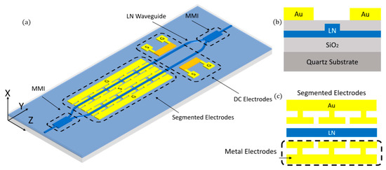
Figure 1.
(a) Schematic diagram of LN modulator chip. (b) Cross-sectional view of the segmented electrodes. (c) Top view of the segmented electrodes.
We observe that, in practice, bandwidth and voltage performance are limited by the following four key factors: first, microwave losses in the transmission line cause the driving voltage to decay over the electrode’s length; second, design trade-offs cause a reduction in electro-optical modulation efficiency; third, design trade-offs reduce modulation efficiency per unit length, requiring larger device sizes to achieve low drive voltages, further limiting bandwidth; and finally, impedance mismatch between the device and external circuitry can also cause problems, such as reflections, and the driving voltage deteriorates. In other words, in order to achieve a high bandwidth and low voltage for the LN modulator, the microwave loss (i.e., the attenuation of the current flowing along the traveling wave direction) should be as low as possible; the effective index of the RF signal should match the group index of the optical signal [20]; the electric field strength between the signal electrode and the ground electrode needs to be strengthened to facilitate effective matching and accumulation of the modulation phase along the traveling-wave direction; and the LN modulator should match the impedance of the external drive circuit to effectively transmit power to the transmission line.
There are two main sources of microwave electrode loss, namely the absorption loss of the substrate and the ohmic conductor loss. Ohmic losses are caused by the finite resistivity of metals and are the dominant loss mechanism in existing thin-film LN modulators. T-shaped traveling wave electrodes with microstructure can allow electrodes to be more evenly distributed over the electrode area. At the same time, it can effectively limit the current within the electrode area and will not enter the electrode gap. This increases the effective conductor area and reduces ohmic losses. Microwave transmission losses are reduced, resulting in greater bandwidth.
We also need the effective refractive index of microwaves and the group refractive index of light waves to be as close as possible. This means that microwaves can travel along transmission lines at the same speed as light waves. Compared with traditional rectangular electrode designs, the microwave speed of segmented electrodes is significantly reduced, known as the slow-wave effect. This is due to the increase in capacitance per unit length of the segmented electrode during each cycle. Therefore, by fine-tuning the size of the T-shaped segmented electrode, the capacitance value per unit length of the electrode can be changed. In addition, the slow-wave effect is used to accurately match the microwave phase velocity and optical group velocity. However, for thin-film LN on a SOI substrate, additional capacitance is introduced due to the T-shaped electrode structure and the slow-wave effect caused by the silicon substrate. These two points together cause the microwave phase velocity to be smaller than the optical group velocity. At this point, the slow-wave effect will cause the velocity mismatch to reappear. Therefore, we use a substrate with a lower dielectric constant, namely a quartz substrate, to reduce the adverse impact of the slow-wave effect.
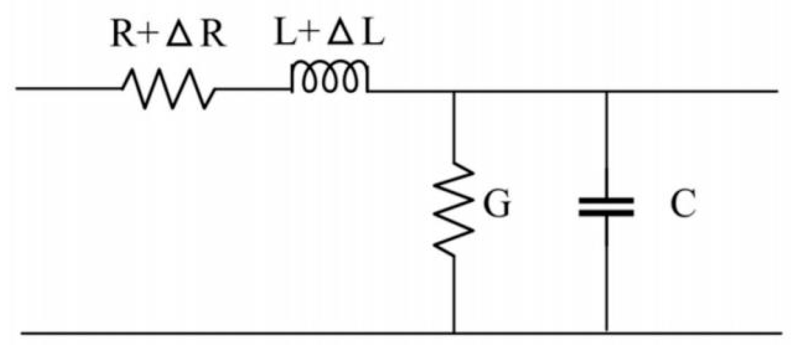
Therefore, segmented structures can be designed to achieve precise matching of microwave speed and light-wave speed. The equivalent circuit of the transmission line is shown in Figure 2. R, C, G and L in the figure are the impedance, capacitance, conductance and inductance of the coplanar waveguide per unit length, respectively. ΔR and ΔL are the impedance and inductance per unit length due to the periodic grooves. According to the theoretical analysis of transmission lines [21], the characteristic impedance Zc and microwave index nm are
where c is the speed of light in vacuum, is the angular frequency and , and are the attenuation constant, phase constant and propagation constant, respectively.

Figure 2.
Transmission line equivalent circuit model of the electrode.
At frequencies above 10 GHz, inductance and capacitance become dominant in (1) and (2) ( and ); then, we have:
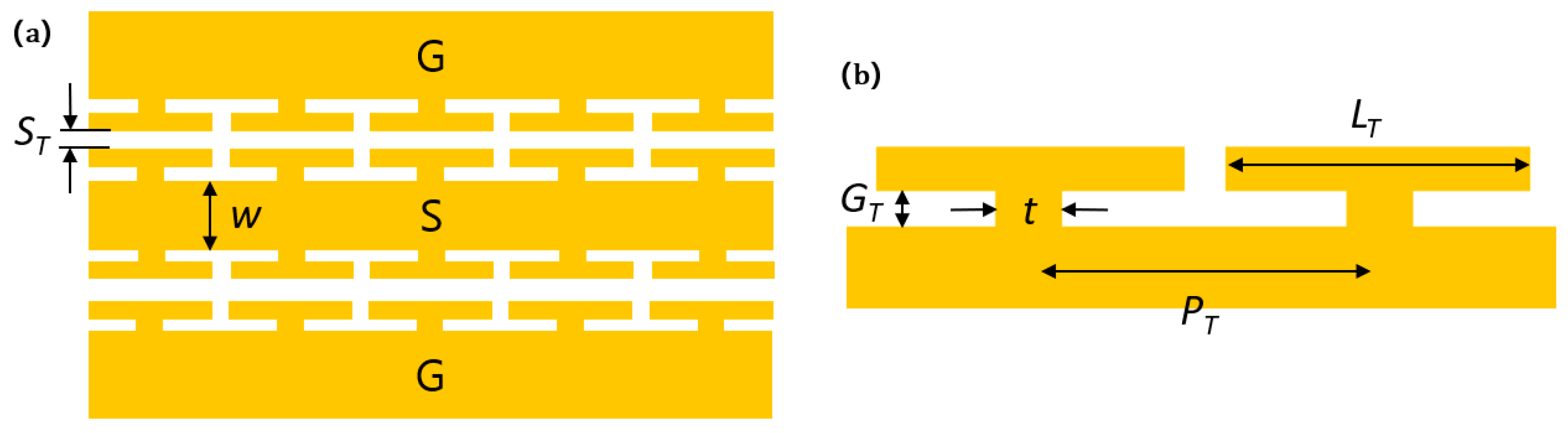
Figure 3 shows the top and partial views of the segmented electrode with the design parameters marked. It can be seen from Equation (4) that the periodic electrode gap will cause an additional inductance ΔL, which will significantly increase the microwave index. That is, the periodic electrode gap can slow down the speed of the microwave signal, thereby achieving wave speed matching. We set the target value of Zc to 50 Ω and then modified the nm value to match the optical index ng. Therefore, the demand values of L+ΔL and C can be calculated by Equation (4). When the electrode gap width is determined, the value of C is mainly affected by the width of the signal electrode. C can be accurately calculated by conformal transformation and quasi-TEM analysis [22]. Then, with C and L known, appropriate parameters can be chosen to obtain the desired ΔL. However, the electromagnetic field in the gap region is not quasi-TEM mode. At the same time, the fringe field around the edge of the gap is complex. Therefore, it is difficult to obtain analytical formulas for ΔR and ΔL. In previous studies on capacitively loaded segmented electrode structures [13,15], the precise value of capacitive load was obtained by fitting the model with experimental results. Here, in order to obtain accurate values of ΔR and ΔL, a commercial 3D electromagnetic simulator is used to perform numerical finite element simulation.
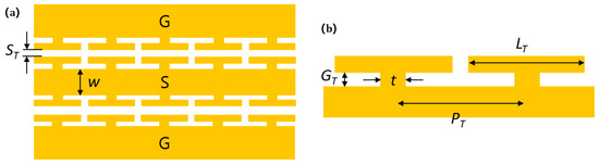
Figure 3.
(a) Top and (b) partial view of the segmented electrode with design parameters labeled.
The height of the electrode was set to 0.9 μm. This was determined through the process. We first used SI9000 software V7.1.0 to calculate the widths of the signal electrode and the ground electrode which were w = 42 μm and Wg = 80 μm, respectively. At this point, the impedance of the electrode is approximately 50 Ω. The two parameters of signal electrode trench length PT and width w have a significant impact on microwave parameters. Therefore, they are the main variable parameters in our design. Other parameters involved in the electrode structure were preliminarily set as follows: PT = 50 μm, WT = 3 μm, GT = 3 μm, t = 2 μm, ST = 3 μm. It is worth noting that if a larger microwave effective refractive index needs to be achieved, a larger gap width GT and a smaller period PT may need to be selected. The reverse is also true.
The segmented structure is designed to achieve precise matching of microwave speed and light-wave speed. The key to obtaining the required nm is to choose appropriate LT and w values. In addition, it is worth noting that as the width of the signal electrode increases, the slot inductance ΔL decreases rapidly. But capacitor C rises much more slowly. Therefore, contrary to conventional CPW, the microwave index nm of the segmented electrode structure does not increase but decreases with increasing signal width.
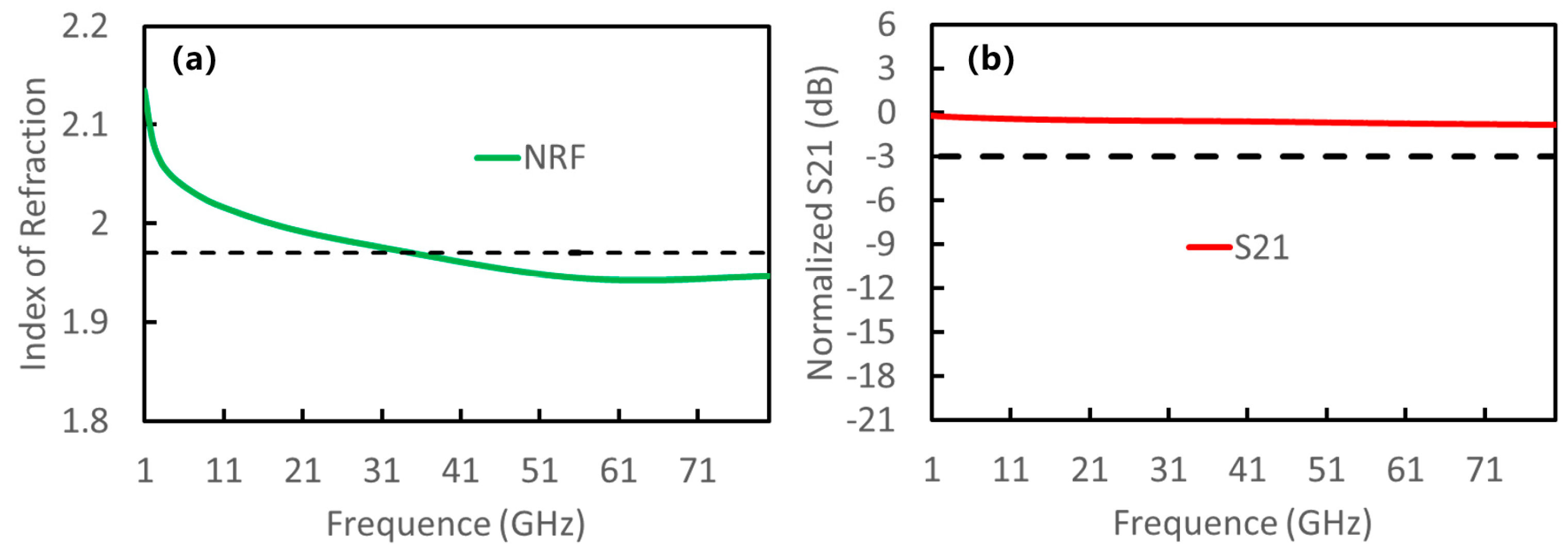
We simulated the S-parameters and microwave refractive index of multiple sets of structural parameters through finite element analysis and ultimately determined the parameters as follows: PT = 50 μm, LT = 47 μm, GT = 3 μm, t = 2 μm, WT = 3 μm, ST = 3 μm. The results are shown in Figure 4. According to the analysis of the optimization results of TWE, the RF group index value is approximately equal to the group index of the LN waveguide, achieving accurate rate matching. In the 0–80 GHz frequency range, the microwave RF index is 1.97. The design simultaneously achieves extremely low attenuation (α) and a characteristic impedance (Z0) match of nearly 50 Ω to reduce RF reflections.
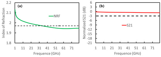
Figure 4.
(a) Effective refractive index of segmented electrodes. (b) S-parameters of segmented electrodes.
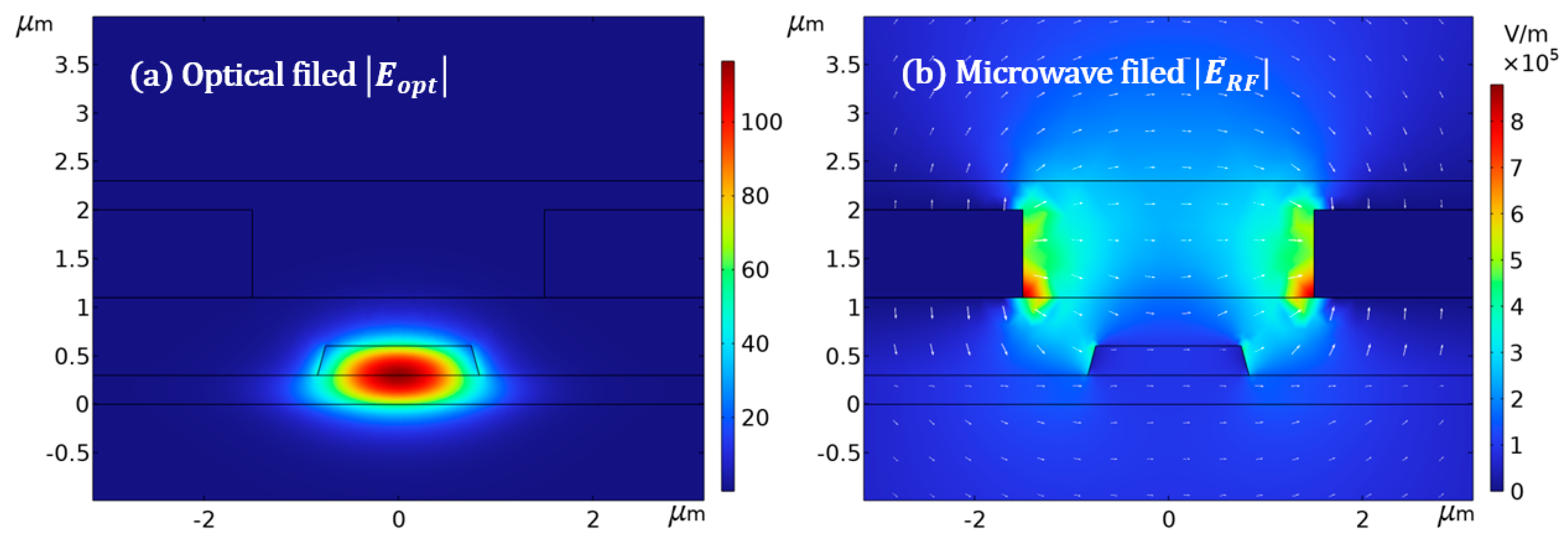
On the other hand, since the design of the optical waveguide and microwave electrode will affect the electro-optical modulation after an electric field is applied, in order to achieve matching of the microwave light-wave mode field, the modulation arm cross section needs to be analyzed. After the electrode is designed, the phase shift caused by the external electric field is related to the overlap integration factor of the electric field and the light field, which means that the relative position of the electrode and the waveguide will have a great impact on it. To increase the electric field strength in the waveguide, we placed electrodes on the flat plate of the LN ridge waveguide. The modulation efficiency of the electrodes increases as the electrode spacing decreases, but the electrode spacing cannot be reduced infinitely. When metal is close to the waveguide area, the metal will produce an absorption effect on the light waves. This further increases the transmission loss of the waveguide. We chose the electrode spacing to be 3 μm, at which the metal absorption mode does not appear.
Metal-induced optical loss varies with the cladding thickness in the area where the waveguide and electrode overlap. The loss is not significant when the cladding thickness exceeds 800 nm, so the cladding thickness of this structure was set to 800 nm. Furthermore, replacing the air cladding with silica cladding improves the electric field distribution inside the waveguide, thereby increasing the electro-optical interaction efficiency. We set the modulation length to 8 mm and the entire device length to 10 mm to achieve a lower drive voltage. Figure 5 shows the electric and optical fields in the waveguide. The corresponding Γ = 29.40%. The calculation method can be found in the references [23].

Figure 5.
The z component of the optical field and the electric field within the waveguide.
Instead of using a DC electro-optical bias controller, we used a TO bias controller built into the LN part shown in Figure 1a. LN has a thermo-optical effect (dneff/dT = 3.34 × 10⁻⁵ K−1 at 1523 nm and 300 K wavelength) [24]. In addition, due to the inherent piezoelectricity and pyroelectric effect of the material, LN will experience DC bias point drift when a static electric field is introduced. This is widely recognized. Feedback compensation control is more complex, but the pyroelectric effect will not be affected by this. The TO solution also eliminates the need for RF bias tees, making packaging and testing more convenient. We can clearly see the advantages of the TO bias controller. Not only is it small in size and high in efficiency, but it can also greatly improve the stability of the bias point and effectively solve the problem of bias drift. This TO bias controller is constructed from two materials. Lithium niobate serves as the waveguide, and the laterally moving heating electrode on the SiO2 cladding is composed of nickel–chromium. Then, the change in optical phase with temperature at this time can be expressed as
where L is the device length, λ0 is the free-space wavelength and ΔT is the temperature change. Considering that the resistor is located above the cladding, the gap between the nichrome metal and the waveguide does not cause optical loss but affects heat conduction and temperature distribution. The thickness and width of the NiCr heating resistor in the TO phase shifter were set to 160 nm and 3 μm, respectively, while the length of the overall phase shifter was set to 200 μm. And the resistance was set to 600 Ω. The corresponding power consumption corresponding to the π phase shift is about 160 mW.
3. Fabrication and Packaging
3.1. Fabrication
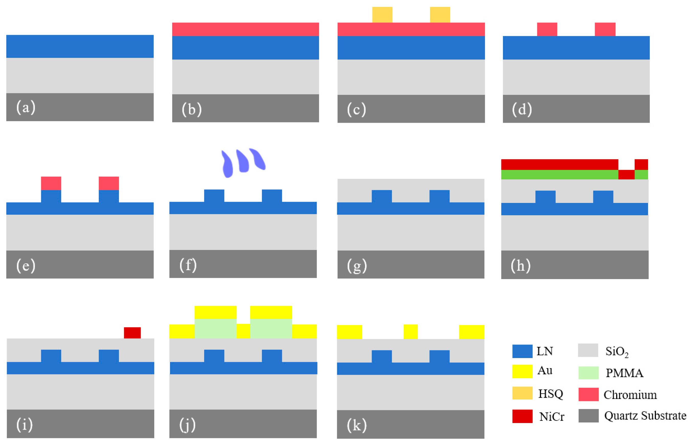
The device is made of an X-cut LN-on-insulator (LNOI) substrate (NANOLN). A 360 nm thick LN film was bonded to a 2 μm thick silicon dioxide insulating layer. The thin-film lithium niobate modulator preparation process we adopt is mainly divided into six main parts, namely cleaning, electron beam exposure, hard mask preparation, waveguide etching, cladding deposition and (thermal) electrode preparation. First, a layer of metallic Cr was deposited on LNOI using the electron beam evaporation method as a hard etch mask with a thickness of 200 nm. Electron beam lithography (EBL) is a widely used semiconductor chip preparation process. The EBL here is mainly used to form the designed waveguide pattern on the hydrogen silsesquioxane polymers (HSQ). The arrangement of the waveguide pattern ensures that the transmission direction of the optical signal is perpendicular to the Z-axis direction of the LN crystal, so that the maximum second-order electro-optical coefficient can be utilized. We then relied on conventional ICP-RIE etching technology to transfer the pattern to the chromium layer, followed by transfer to the LN via an argon gas mixture flowing through the ICP-RIE process following an optimized etching recipe [25]. The etching rate was set to about 30 nm/min. The sidewall inclination angle of the lithium niobate waveguide is greater than 75°, and the etching depth is 0.180 μm. Next, PECVD technology was used to deposit a silicon dioxide cladding layer with a thickness of 700 nm on the top of the LN waveguide. The nickel–chromium metal resistors were then deposited by electron beam and formed along the straight arms of the MZI using a standard lift-off process. Similarly, gold electrodes were also made through a second EBL alignment, evaporation and demolding process. Finally, the finished device was cut and finely polished to ensure proper coupling between the fibers. The entire process flow is shown in Figure 6. SEM and optical microscope images of the high-speed lithium niobite EO modulation region are shown in Figure 7.
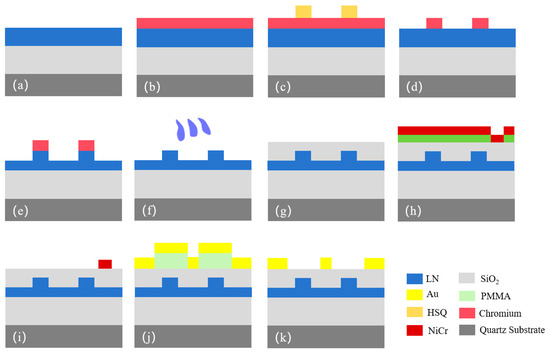
Figure 6.
Schematic diagram of the process. (a) Chip cleaning. (b) Deposition of Chromium. (c) HSQ etching. (d) Chromium etching. (e) LN waveguide etching. (f) Chromium removal. (g) Deposition of silica cladding. (h) Deposition of nickel-chromium metal. (i) PMMA patterning and nickel-chromium metal deposition. (j) PMMA patterning and gold deposition. (k) PMMA stripping.
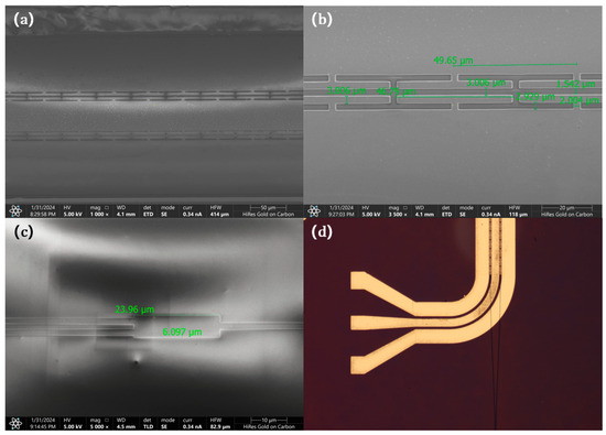
Figure 7.
Scanning electron microscope images and optical microscope images of the fabricated device: (a,b) SEM images of segmented electrodes; (c) SEM image of MMI; (d) optical microscope image of electrode corners.
3.2. Packaging
High-performance packaging of modems requires consideration of several key aspects, such as optical performance, electrical performance, mechanical performance and hermeticity. Figure 8 gives an internal view of the packaged modulator to illustrate how these issues can be addressed.
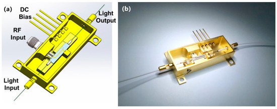
Figure 8.
(a) Schematic diagram and (b) real shots of the internal structure of the packaged EO modulator.
The package size is 45 mm × 20 mm × 9 mm. We chose Kovar as the encapsulation material because of its good thermal expansion compatibility with fiber optics, traditional glass-to-metal seals and ceramic feedthroughs. The package surface is nickel-plated and gold-plated. The interior of the Kovar package is machined to make room for the lithium niobate chip and ceramic electronic components. These parts serve as microwave inputs and terminals. The two ports within the package for optical feedthrough are soldered using Kovar tubes.
After analysis, the coupling process between the optical mode field in the lithium niobate waveguide and the optical mode field in the optical fiber is the main cause of optical loss. Compared with the optical mode field in optical fibers, the optical mode field in the optical waveguides of lithium niobate film is very small. Therefore, in order to reduce the cross-scale optical coupling loss between the fiber and the chip, we chose a polarization-maintaining fiber with a smaller core diameter. And an SSC was built on the chip end-face to achieve the best match of mode field size and distribution. The lateral and angular alignment of the fiber core relative to the waveguide requires tolerances of approximately 0.1 μm and 0.05 μm. In this experiment, we used a high-precision six-dimensional coupling platform with an accuracy of 10 nm and 0.01 degree for optical coupling.
The polarization axis of the PMF is rotated to align features on the glass tube. During the entire optical alignment and installation process, in order to achieve a fixation effect, the glass tube is installed and adjusted relative to the lithium niobate mold so that it is stably attached to the mold surface. The entire process requires active alignment of the input and output fibers to occur simultaneously. The optical fiber is then attached to the tube using a commercially available index-matching adhesive and UV epoxy. We use RMA flux and eutectic solder to solder the sealed splice on the fiber into the sealed tube and remove it when complete. The design of the sealed tube, the selection of solder and the establishment of welding technology are all to ensure that the PMF can withstand moderate radial stress to maintain a high polarization extinction ratio greater than 20 dB. The theoretically calculated optical loss is 10 dB, and the actual coupling loss is about 20 dB.
Due to RF design and module assembly accuracy, problems such as impedance mismatch or grounding discontinuity may occur on the RF signal transmission route of the packaged device. For example, the assembly of RF connectors and the transition area between electro-optic chips and packages. In order to obtain good EO performance, a 1.85 mm connector with a useful bandwidth of approximately 65 GHz is used. During the assembly and packaging process, the concentricity error of the connector glass beads in the Kovar housing must be controlled to prevent undesirable resonances.
The electro-optic system includes a Kovar heat sink, RF connectors and RF thin-film transmission circuitry. In order to reduce RF loss and matching impedance, the installed grounded coplanar waveguide transmission line must meet RF transmission characteristics. The RF signal is coupled to the modulator through an external V-connector and then connected to a coplanar waveguide (CPW) transmission line printed on an ALN substrate. The modulator is soldered to the ALN substrate. A gold wire is used to make the electrical connection to the modulator. ALN not only has a low RF loss tangent (0.03 at 10 GHz), but it also has extremely high thermal conductivity (285 W/dc degrees Celsius) to aid thermal management.
A strong connection between MSL and glass beads will maximize RF performance. However, during assembly, a valid ground connection must be established between the substrate and package sidewalls. If there is an air gap between these two components, A ground discontinuity will occur in this transition zone. In addition to the CPW transmission lines, 50 Ω thin-film termination resistors are used in the sub-installation. This terminating resistor is contacted using tape adhesive and is necessary to produce excellent return loss. By partially capacitating the resonant modulator, the inductance of the ribbon bond can be exploited to improve the return loss of the device.
After seam-sealing the Kovar lid to the outer casing, the package is complete. The lids were seam-sealed using commercially available parallel gap welding equipment. After fiber connections and welding seals are completed, standard helium leak detection equipment is used to test the tightness of the packaging device and fluorine oil is used for rough leak detection.
4. Results and Discussion
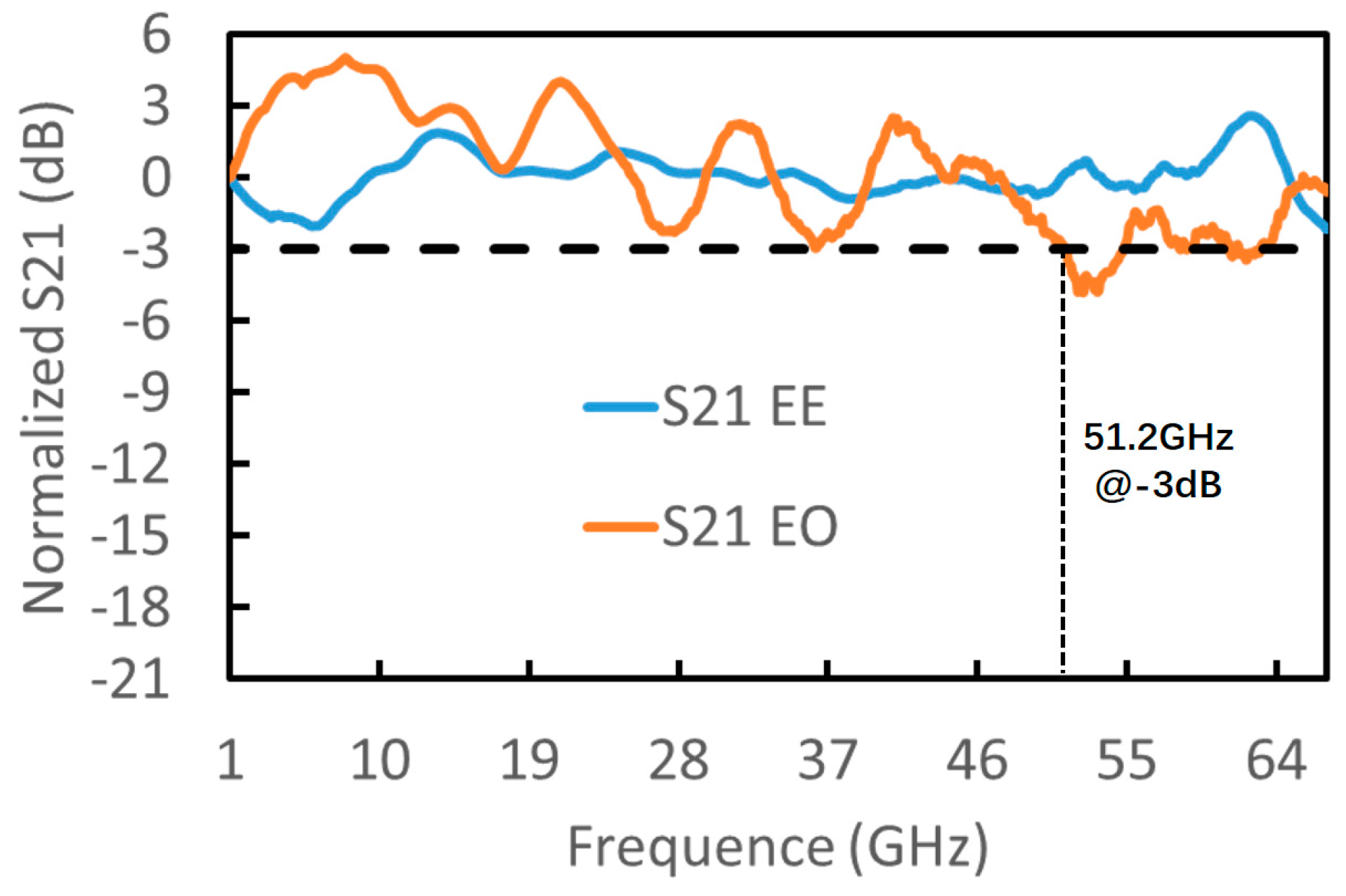
We measured the frequency response of the designed modulator via a 67 GHz network analyzer. The results are shown in Figure 9. The actual measured 3 dB EE bandwidth is higher than 67 GHz and the 3 dB EO bandwidth is 51.2 GHz. Next, we performed TO and EO characterization using a tunable-wavelength laser source in the communication C-band. The results are as expected. Due to the large TO coefficient of lithium niobate material, TO phase shifters show high efficiency. The Vπ of a nickel-chromium heating electrode is approximately 3.5 V. The observed extinction ratio is approximately 15 dB. EO Vπ measurements are made by performing a 100 kHz triangular voltage sweep across the device. The response shows a Vπ of 10.25 V for the 8 mm long device.
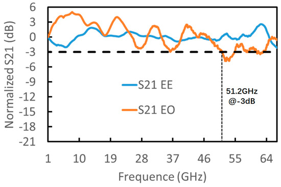
Figure 9.
Measured EE bandwidth and EO bandwidth.
At a wavelength of 1550 nm, the insertion loss of our packaged devices is measured to be −20 dB. This is quite different from theoretical analysis, which we believe is due to the sidewall roughness caused by etching, resulting in significant scattering loss, and the displacement of the optical fiber during the curing process, which is inevitable during packaging. Insertion loss can be reduced by improving the SSC structure and etching process.
The device underwent mechanical impact testing in accordance with GJB 548B-2005. (Test condition A: 500 g, 1.0 ms, direction Y1, five times). After the experiment, there was no significant damage to the surface of the sample, and there were no metal wires falling off or folding. The device was leak tested according to GJB 128A-1997 (Test condition D: fluorine oil, temperature: 85 °C). There were no two or more bubbles generated at the same point of the shell sealing weld, and no bubbles with increased attachment were generated. The experimental results meet the sealing performance requirements of electronic components.
In recent years, most of the reports on thin-film lithium niobate electro-optic modulators have been based on direct testing of bare chips using high-frequency probes on a coupling platform. Compared to these bare chips, the performance of our fabricated devices is not outstanding, but it is noteworthy that our devices are metal-encapsulated and have passed reliability testing, which is very rare in related reports. We believe that this work will provide guidance for researchers interested in the process of manufacturing such devices.
5. Conclusions
The modulator we manufactured achieves a 51.2 GHz 3 dB EO bandwidth. Meanwhile, we maintained an on-chip loss of <2 dB and a high extinction ratio of 15 dB. It is worth noting that the devices we manufactured were metal-encapsulated and passed a series of reliability tests. The success of this modulator module marks a crucial step forward in the productization and application of thin-film lithium niobate modulation devices.
Author Contributions
Conceptualization, J.T. and Y.Y.; methodology, J.T. and Y.Y.; software, J.T. and P.W.; validation, J.T., Y.Y. and X.L.; formal analysis, X.L. and P.W.; writing—original draft preparation, Y.Y.; writing—review and editing, J.L. (Jinye Li) and J.T.; project administration, J.L. (Jianguo Liu), J.T. and Y.Y. made equal contributions to this work. All authors have read and agreed to the published version of the manuscript.
Funding
This research was funded by the National Natural Science Foundation of China (NSFC), grant number 62035009.
Institutional Review Board Statement
Not applicable.
Informed Consent Statement
Not applicable.
Data Availability Statement
Data underlying the results presented in this paper are not publicly available at this time but may be obtained from the authors upon reasonable request.
Conflicts of Interest
The authors declare no conflicts of interest.
References
- Reed, G.T.; Mashanovich, G.; Gardes, F.Y.; Thomson, D.J. Silicon optical modulators. Nat. Photonics 2010, 4, 518–526. [Google Scholar] [CrossRef]
- Mastronardi, L.; Banakar, M.; Khokhar, A.Z.; Hattasan, N.; Rutirawut, T.; Bucio, T.D.; Grabska, K.M.; Littlejohns, C.; Bazin, A.; Mashanovich, G. High-speed Si/GeSi hetero-structure electro absorption modulator. Opt. Exp. 2018, 26, 6663–6673. [Google Scholar] [CrossRef] [PubMed]
- Ogiso, Y.; Ozaki, J.; Ueda, Y.; Wakita, H.; Nagatani, M.; Yamazaki, H.; Nakamura, M.; Kobayashi, T.; Kanazawa, S.; Hashizume, Y.; et al. 80-GHz bandwidth and 1.5-v vπ InP-based IQ modulator. J. Lightw. Technol. 2020, 38, 249–255. [Google Scholar] [CrossRef]
- Lange, S.; Wolf, S.; Lutz, J.; Altenhain, L.; Schmid, R.; Kaiser, R.; Schell, M.; Koos, C.; Randel, S. 100 gbd intensity modulation and direct detection with an InP-based monolithic DFB laser Mach-Zehnder modulator. J. Lightw. Technol. 2018, 36, 97–102. [Google Scholar] [CrossRef]
- Witzens, J. High-speed silicon photonics modulators. Proc. IEEE 2018, 106, 2158–2182. [Google Scholar] [CrossRef]
- Xu, H.; Xiao, X.; Li, X.; Hu, Y.; Li, Z.; Chu, T.; Yu, Y.; Yu, J. High speed silicon Mach-Zehnder modulator based on interleaved PN junctions. Opt. Exp. 2012, 20, 15093–15099. [Google Scholar] [CrossRef] [PubMed]
- Xu, H.; Li, X.; Xiao, X.; Zhou, P.; Li, Z.; Yu, J.; Yu, Y. High-speed silicon modulator with band equalization. Opt. Lett. 2014, 39, 4839–4842. [Google Scholar] [CrossRef]
- Li, M.; Wang, L.; Li, X.; Xiao, X.; Yu, S. Silicon intensity Mach-Zehnder modulator for single lane 100 Gb/s applications. Photonics Res. 2018, 6, 109–116. [Google Scholar] [CrossRef]
- Wolf, S.; Zwickel, H.; Kieninger, C.; Lauermann, M.; Hartmann, W.; Kutuvantavida, Y.; Freude, W.; Randel, S.; Koos, C. Coherent modulation up to 100 GBd 16QAM using silicon-organic hybrid (SOH) devices. Opt. Exp. 2018, 26, 220–232. [Google Scholar] [CrossRef]
- Alloatti, L.; Palmer, R.; Diebold, S.; Pahl, K.P.; Chen, B.; Dinu, R.; Fournier, M.; Fedeli, J.M.; Zwick, T.; Freude, W.; et al. 100 GHz silicon-organic hybrid modulator. Light Sci. Appl. 2014, 3, e173. [Google Scholar] [CrossRef]
- Xu, M.; Chen, W.; He, M.; Wen, X.; Ruan, Z.; Xu, J.; Chen, L.; Liu, L.; Yu, S.; Cai, X. Michelson interferometer modulator based on hybrid silicon and lithium niobate platform. APL Photonics 2019, 4, 100802. [Google Scholar] [CrossRef]
- Weigel, P.O.; Zhao, J.; Fang, K.; Al-Rubaye, H.; Trotter, D.; Hood, D.; Mudrick, J.; Dallo, C.; Pomerene, A.T.; Starbuck, A.L. Bonded thin film lithium niobate modulator on a silicon photonics platform exceeding 100 GHz 3-db electrical modulation bandwidth. Opt. Exp. 2018, 26, 23728–23739. [Google Scholar] [CrossRef] [PubMed]
- Rao, A.; Patil, A.; Rabiei, P.; Honardoost, A.; DeSalvo, R.; Paolella, A.; Fathpour, S. High-performance and linear thin-film lithium niobate Mach-Zehnder modulators on silicon up to 50 GHz. Opt. Lett. 2016, 41, 5700–5703. [Google Scholar] [CrossRef] [PubMed]
- Jin, S.; Xu, L.; Zhang, H.; Li, Y. LiNbO3 thin-film modulators using silicon nitride surface ridge waveguides. IEEE Photonics Technol. Lett. 2016, 28, 736–739. [Google Scholar] [CrossRef]
- Wang, C.; Zhang, M.; Chen, X.; Bertrand, M.; Shams-Ansari, A.; Chandrasekhar, S.; Winzer, P.; Lončar, M. Integrated lithium niobate electro-optic modulators operating at cmos-compatible voltages. Nature 2018, 562, 101–104. [Google Scholar] [CrossRef]
- Wang, C.; Zhang, M.; Stern, B.; Lipson, M.; Loncar, M. Nanophotonic lithium niobate electro-optic modulators. Opt. Exp. 2018, 26, 1547–1555. [Google Scholar] [CrossRef] [PubMed]
- Honardoost, A.; Juneghani, F.A.; Safian, R.; Fathpour, S. Towards subterahertz bandwidth ultracompact lithium niobate electrooptic modulators. Opt. Exp. 2019, 27, 6495–6501. [Google Scholar] [CrossRef] [PubMed]
- He, M.; Xu, M.; Ren, Y.; Jian, J.; Ruan, Z.; Xu, Y.; Gao, S.; Sun, S.; Wen, X.; Zhou, L.; et al. High-performance hybrid silicon and lithium niobate Mach-Zehnder modulators for 100 gbits-1 and beyond. Nat. Photonics 2019, 13, 359–364. [Google Scholar] [CrossRef]
- Arizmendi, L. Photonic applications of lithium niobate crystals. Phys. Status Solidi 2004, 201, 253–283. [Google Scholar] [CrossRef]
- Aoki, K.; Kondou, J.; Mitomi, O.; Minakata, M. Velocity-matching conditions for ultrahigh-speed optical LiNbO3 modulators with traveling-wave electrode. Jpn. J. Appl. Phys. 2006, 45, 8696–8698. [Google Scholar] [CrossRef]
- Collin, R.E. Foundations for Microwave Engineering; McGraw-Hill: New York, NY, USA, 1966. [Google Scholar]
- Carlsson, E.; Gevorgian, S. Conformal mapping of the field and charge distributions in multilayered substrate CPWs. IEEE Trans. Microw. Theory Tech. 1999, 47, 1544–1552. [Google Scholar] [CrossRef]
- Huang, X.; Liu, Y.; Li, Z.; Guan, H.; Wei, Q.; Yu, Z.; Li, Z. Advanced Electrode Design for Low-Voltage High-Speed Thin-Film Lithium Niobate Modulators. IEEE Photonics J. 2021, 13, 7900609. [Google Scholar] [CrossRef]
- Moretti, L.; Iodice, M.; Della Corte, F.G.; Rendina, I. Temperature dependence of the thermo-optic coefficient of lithium niobate, from 300 to 515 K in the visible and infrared regions. J. Appl. Phys. 2005, 98, 036101. [Google Scholar] [CrossRef]
- Li, D.; Li, J.; Li, R.; Liu, J. The Design and Characterization of an Ultra-Compact Asymmetrical Multimode Interference Splitter on Lithium Niobate Thin Film. Photonics 2024, 11, 60. [Google Scholar] [CrossRef]


Disclaimer/Publisher’s Note: The statements, opinions and data contained in all publications are solely those of the individual author(s) and contributor(s) and not of MDPI and/or the editor(s). MDPI and/or the editor(s) disclaim responsibility for any injury to people or property resulting from any ideas, methods, instructions or products referred to in the content. |
© 2024 by the authors. Licensee MDPI, Basel, Switzerland. This article is an open access article distributed under the terms and conditions of the Creative Commons Attribution (CC BY) license (https://creativecommons.org/licenses/by/4.0/).