Abstract
Numerous optoelectronic devices based on low-dimensional nanostructures have been developed in recent years. Among these, pyramidal low-dimensional semiconductors (zero- and one-dimensional nanomaterials) have been favored in the field of optoelectronics. In this review, we discuss in detail the structures, preparation methods, band structures, electronic properties, and optoelectronic applications (photocatalysis, photoelectric detection, solar cells, light-emitting diodes, lasers, and optical quantum information processing) of pyramidal low-dimensional semiconductors and demonstrate their excellent photoelectric performances. More specifically, pyramidal semiconductor quantum dots (PSQDs) possess higher mobilities and longer lifetimes, which would be more suitable for photovoltaic devices requiring fast carrier transport. In addition, the linear polarization direction of exciton emission is easily controlled via the direction of magnetic field in PSQDs with C3v symmetry, so that all-optical multi-qubit gates based on electron spin as a quantum bit could be realized. Therefore, the use of PSQDs (e.g., InAs, GaN, InGaAs, and InGaN) as effective candidates for constructing optical quantum devices is examined due to the growing interest in optical quantum information processing. Pyramidal semiconductor nanorods (PSNRs) and pyramidal semiconductor nanowires (PSNWRs) also exhibit the more efficient separation of electron-hole pairs and strong light absorption effects, which are expected to be widely utilized in light-receiving devices. Finally, this review concludes with a summary of the current problems and suggestions for potential future research directions in the context of pyramidal low-dimensional semiconductors.
1. Introduction
1.1. Structures and Properties of Low-Dimensional Nanomaterials
Nanotechnology is the science of studying the interactions, compositions, properties, and manufacturing of materials at the nanoscale (i.e., from atoms and molecules to the submicron scale) [1,2,3,4,5,6,7,8,9,10]. With the ongoing development of nanotechnology, the structures and properties of nanomaterials have gradually attracted the attention of researchers. Low-dimensional nanomaterials are those that have at least one dimension in the nanoscale range (1–100 nm) [11]. Importantly, such materials exhibit physical and chemical characteristics that differ from those of conventional materials. Low-dimensional nanomaterials have unique structures, and as a result, they do not possess the properties of traditional block materials; this is an important basis for the development of nanoscience and technology. More specifically, the unique structures of low-dimensional nanomaterials produce a range of effects, including surface, small-size, quantum-size, and macroscopic quantum tunneling effects [12,13,14,15]. Consequently, low-dimensional nanomaterials exhibit unique characteristics in terms of their magnetic, optical, electrical, thermal, and sensing properties [16,17,18,19,20]. Low-dimensional nanomaterials can be divided into zero-, one-, and two-dimensional nanomaterials, depending on their dimensions. Zero-dimensional nanomaterials include clusters, quantum dots (artificial atoms, QDs), and nanoparticles [21,22,23]; one-dimensional nanomaterials include nanowires (NWRs), nanorods (NRs), nanotubes, and nanofibers [24,25,26,27]; and two-dimensional nanomaterials include nanoribbons, ultra-thin films, and multilayer membranes [28,29,30].
1.2. Influences of Low-Dimensional Semiconductor Morphologies on Optoelectronics
In this review, we consider the effects of the morphologies and dimensions of pyramidal low-dimensional semiconductors on their application in the field of optoelectronics. In Figure 1, pyramidal low-dimensional semiconductors include pyramidal semiconductor quantum dots (PSQDs), pyramidal semiconductor clusters, pyramidal semiconductor nanorods (PSNRs), and pyramidal semiconductor nanowires (PSNWRs) [31,32,33,34]. Broadly speaking, truncated PSQDs, PSNRs, and PSNWRs can also be considered as pyramidal low-dimensional semiconductors, whereas their crystal planes at the tip are parallel to the bottom planes. Moreover, material morphology has become an important direction for the development of materials science within nanomaterials research [35,36]. Morphology produces significant effects on various characteristics in these systems (e.g., optics, electricity, and magnetism) via thermodynamics, kinetics, and crystallography [37,38,39]. However, so far, there is still no unified theory for the study of the photoelectric properties of nanomaterials with different morphologies. Because the optical properties of low-dimensional semiconductors are strongly dependent on the shapes and interaction between nanoparticles, the band structures can be adjusted by changing morphologies and sizes to optimize the photoelectric performance [40]. In addition, quantum confinement effects can change the band gap of most semiconductors to achieve a wide and continuously adjustable range [41].
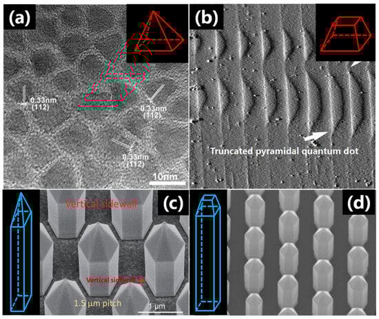
Figure 1.
Different pyramidal low-dimensional materials: (a) a pyramidal semiconductor quantum dot (PSQD) [31]; (b) a truncated pyramidal semiconductor quantum dot (truncated PSQD) [32]; (c) a pyramidal semiconductor nanorod (PSNR), or a pyramidal semiconductor nanowire (PSNWR) [33]; and (d) a truncated pyramidal semiconductor nanorod (truncated PSNR), or a truncated pyramidal semiconductor nanowire (truncated PSNWR) [34].
According to their geometric shapes, QDs can be divided into spherical, tetrahedral (pyramidal), cylindrical, disk, and plate QDs, among others [42]. Common QD materials include CdS, CdSe, CdTe, and ZnS, which represent II-VI semiconductor QDs [43]; PbS and PbSe, which represent IV–VI semiconductor QDs [44]; and InP, GaAs, and InAs, which represent III–V semiconductor QDs [45]. Although PSQDs contain similar material components, III–V pyramidal nanostructures exhibit superior thermal stabilities [46]. Since Lopez et al. first reported pyramidal GaAs QDs, PSQDs with various components have been successfully prepared [47]. For nearly half a century, the application of semiconductor QDs in optoelectronics has led to significant advances, and optoelectronic devices constructed using PSQDs have also undergone remarkable developments [48,49,50]. Compared with spherical and plate QDs, PSQDs have different degrees of electron and hole confinement and different k-space composition of their wave functions due to the nontrivial interplay between the geometric configurations and composition of material surfaces in various shapes, which is considered to be the possible reason for the difference in optical properties [51,52]. Moreover, compared with PSQDs, spherical and plate QDs exhibit faster radiative and slower Auger recombination times with similar emission energy, making them more suitable for applications in lasers and light-emitting devices [53,54]. PSQDs possess higher mobilities and longer lifetimes, which would be suited for applications in field-effect transistors and photovoltaic devices requiring fast carrier transport [53]. In addition, PSQDs also have high photoluminescence (PL) efficiency and large specific surface area, which is beneficial to the sensing application [55]. The linear polarization direction of exciton emission is controlled via the direction of the magnetic field in PSQDs with C3v symmetry so that all-optical multi-qubit gates based on electron spin as a quantum bit could be realized [56,57]. Therefore, based on the above viewpoints, we can combine the morphological advantages of PSQDs to develop optoelectronic devices in the fields of photocatalysis, photodetection, solar cells, and optical quantum information. Patterned PSQD arrays are more conducive to the construction of optoelectronic devices compared with common colloidal QDs, indicating their potential application value [58]. More specifically, the photoelectric properties of PSQDs can be effectively improved by component regulation, alloying, and the preparation of core-shell structures [59,60,61]. The maximum photoluminescence quantum yields (PLQYs) of some QDs with different morphologies and components are shown in Table 1.

Table 1.
Maximum PLQYs with different semiconductor QDs and shapes.
Semiconductor NWRs (semiconductor NRs) are unique one-dimensional artificial micro-nano structures that exhibit various advantages over traditional block semiconductor materials and other nanomaterials [77,78,79,80]. For example, NWRs exhibit significant surface and size effects, they are the smallest unit of charge transmission, and they can be used both in device construction units and as the interconnecting wires of device circuits. In addition, semiconductor NWRs have a diverse range of chemical compositions, including GaN, ZnO, and TiO2. Since the first synthesis of Si NWRs, a variety of quasi-one-dimensional NWRs, such as semiconductor NWRs, nanobelts, NRs, and nanotubes, have been successfully prepared and have attracted the attention of researchers [81,82,83,84,85]. Common NWRs can be divided into cylindrical, quadrangular, and hexagonal NWRs, among others. Since Ruach et al. first reported pyramidal CdSe NWRs, PSNWRs with various components have been successfully prepared [86]. Many studies have shown that these quasi-one-dimensional nanomaterials and structures have promising applications in nano-optoelectronic and electronic devices [87,88]. PSNRs and PSNWRs have been applied in the fields of photocatalysis, photodetectors, and solar cells due to their large specific surface area, the more efficient separation of electron-hole pairs, and strong light absorption effects [89,90].
2. Structure, Growth, and Preparation of Pyramidal Low-Dimensional Semiconductors
2.1. Pyramidal Semiconductor Quantum Dots with Different Components
2.1.1. Structure and Growth of Pyramidal SiGe/Si Quantum Dots
In the material systems of pyramidal low-dimensional semiconductors, pyramidal QDs are the most widely studied. Among the many pyramidal QD systems reported to date, self-assembled SiGe/Si QDs possess the simplest epitaxial structures. Based on scanning tunneling microscopy (STM) experimental observations, researchers have discovered that the growth of SiGe/Si self-assembled QDs can be described as follows. Firstly, the growth of Ge or SiGe QDs originates from the instability of the epitaxial plane, which is induced by mismatch strain, and is initially manifested as the fluctuation of only a few atoms on the growth surface. As the epitaxial growth process continues and the deposition amount increases, these surface fluctuations become approximately circular islands that the heights are ~3–4 monolayer (ML). These islands initially possess no definite crystallographic morphology and gradually grow into pyramids surrounded by {105} facets [91,92,93]. During subsequent growth, as their volume increases, these pyramidal growth islands take the shape of a dome or barn with a steeper outer surface (Figure 2) [94]. The outer surface of the dome or barn island contain {105}, {111}, {113}, {15 3 23}, and {20 4 23} facets [95,96]. In addition, the morphological changes from the pyramid to the dome or barn are discontinuous and can be explained by considering a thermodynamic phase-transition model [97]. More specifically, PSQDs exist in the transition state of crystal nucleation; therefore, their thermodynamic state is not stable, and phase transition occurs easily. Although the growth of SiGe/Si self-assembled QDs is influenced by many factors, these conclusions are applicable under a wide range of conditions.
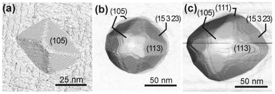
Figure 2.
Growth morphology of a SiGe quantum dot [94]: (a) Pyramid, (b) dome, and (c) barn.
2.1.2. Structure and Growth of Pyramidal III–V Quantum Dots
In the III–V semiconducting QD family, researchers initially focused on InAs/GaAs QDs, which possess a zinc-blende crystal structure with a direct band gap [98]. Additionally, InAs/GaAs QDs, as second-generation semiconductor materials, are expected to exhibit great application potential in optoelectronic devices [99]. To date, researchers have devoted significant efforts to examining the growth and structures of InAs/GaAs QDs. Despite the accumulation of large amounts of experimental data, few conclusions have been formed, likely due to the complexity of the problem. In the InAs/GaAs system, the QD growth process and structure are affected by many factors, such as the atmosphere, growth rate, temperature, deposition method, and material structure. Consequently, the growth conditions should be carefully optimized. In a mathematical sense, optimization is preferably carried out based on numerous permutations and combinations. The growth process of InAs/GaAs(001) QDs was investigated by Xu et al. [100], who considered the complex growth morphologies of pyramidal QDs. They suggest that InAs QDs with different volumes in the same system represent different growth stages. Hence, by observing the morphologies of QDs with different volumes using STM, changes in the QD morphology during the growth process can be carefully deduced. As presented in Figure 3, the initial morphology of the QD is a rhombohedral tetrahedron or pyramid composed of {137}A facets. During the subsequent growth stage, growth along the [110] direction is faster than that along the [10] direction, and as a result, {}B facets appear, followed by {}B facets. When the bottom width of the QD reaches a critical value, the steeper {110}, {111}A, and {}B facets appear successively.
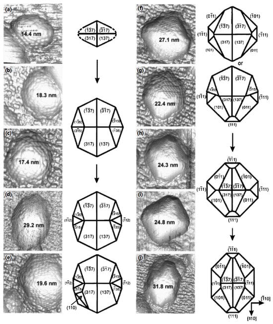
Figure 3.
Schematic outlining the growth process of InAs/GaAs(001) QDs [100]. (a–j) These images show that as the volume of these QDs increases, their shapes are constantly changing.
Considering the above hypothesis, Figure 4a outlines the changes in the cross-sectional morphology of an InAs QD observed along the [111] direction. According to the results of the Liu, Kratzer, and Xu groups [100,101], who used similar experimental methods and perspectives, the initial QD morphology is a pyramid surrounded by {137} facets; as the growth process advances, {110}, {111}, and {} facets begin to appear on the outer surface. By comparing the growth processes of the SiGe/Si self-assembled QD and InAs/GaAs(001) QD systems, it is clear that the two growth processes are similar, following the Stranski–Krastanow growth mode, wherein the pyramidal shape changes in the presence of a phase transition driving force.
Despite these advances, the growth processes of other PSQDs have not been extensively studied. However, progress has been made in the study of the pyramidal structures of AlGaAs/GaAs, InGaAs/AlGaAs, InGaAs/GaAs, and InAs/InP QDs in III–V low-dimensional compound semiconductors. These works are of particular interest due to the attractive development prospects exhibited by AlGaAs/GaAs QDs for application in quantum cascade lasers. The spontaneous growth structure of this type of QD is a typical truncated pyramidal (GaAs(001) substrate) due to the fact that the growth rates of the four {011} facets are slower than those of the low-index facets [102]. In addition, the growth range of the top region of the truncated pyramid is narrower because of the self-limiting growth mechanism. Hartmann et al. successfully prepared inverted pyramidal AlGaAs/GaAs QDs using a pyramidal groove pattern on a GaAs(111)B substrate and realized the controllable preparation of AlGaAs/GaAs QDs [103]. In another study, Pelucchi et al. prepared inverted pyramidal InxGa1−xAs/Al0.30Ga0.70As QDs on a patterned GaAs(111)B substrate, and observed that the growth rate of the QDs is faster at the tip of the pyramid due to surface diffusion on the (111)B plane [104]. In addition, Pelucchi et al. also fabricated inverted-pyramidal InGaAs/GaAs QDs on the same substrate, and in this case, the QDs grew laterally along the crystallographic orientation of the (111)A facet [105]. Prohl et al. successfully prepared truncated pyramidal In0.25Ga0.75As/GaAs QDs on a GaP(001) substrate, whereas the formation of such a shape is related to the occurrence of a capping layer and the intense lateral material transport from the wetting layer into the QDs [106]. Later, Gajjela et al. fabricated truncated pyramidal (InGa)(AsSb)/GaAs QDs on the same GaP substrate [107]. Compared with the work of Prohl et al. [106], the average size of the QDs was smaller due to the reduction in adatom mobility (surfactant effect of Sb) on the growth surface. Hasan et al. prepared InAs/InP QDs on an InP(001) substrate, and discovered that the morphologies of the InAs/InP QDs were related to the QD volume [108]. More specifically, when the volume of the QDs was <104 nm3, the morphology tended to be spherical, and when the volume was >104 nm3, a truncated pyramidal morphology was obtained (Figure 4b).

Figure 4.
(a). Cross-sectional diagram of an InAs QD at different stages of growth, among which numbers (1–6) show the different atomic layers [100]. (b) Schematic representation of the changes in morphology and volume of an InAs/InP QD during growth [108].
Figure 4.
(a). Cross-sectional diagram of an InAs QD at different stages of growth, among which numbers (1–6) show the different atomic layers [100]. (b) Schematic representation of the changes in morphology and volume of an InAs/InP QD during growth [108].

2.1.3. Structure and Growth of Pyramidal III-Nitride Quantum Dots
The III-nitride semiconductor QDs have been reported as direct-gap materials that cover the spectral range from near-infrared to ultraviolet [109]. Such materials are particularly suitable for the development of optoelectronics, especially short-wavelength optoelectronic devices, which can be implemented into high-temperature, high-frequency, and high-power electronic devices. Currently, GaN-based III-nitrides are the most attractive third-generation semiconductor materials [110]. In this context, Korytov et al. prepared GaN QDs with two morphologies on an Al0.5Ga0.5N substrate [111]. More specifically, the growth of the GaN QDs on the surface of Al0.5Ga0.5N led to a pyramidal shape (height = 12 ML) (Figure 5a), whereas when the GaN QDs were embedded in the interior of Al0.5Ga0.5N, a truncated pyramidal shape was obtained (height = 8 ML) (Figure 5b). Furthermore, in the case where the Al0.5Ga0.5N matrix is overgrown, the QD morphology changes dramatically. In addition to pyramidal GaN QDs, InGaAsN is an important material for constructing pyramidal III-nitride semiconductor QDs. However, the strain of the InGaAs layer was found to limit the emission spectrum of the QDs to a wavelength of ~880 nm (calibrated indium concentration = 45%), resulting in poor spectral quality. Consequently, Pelucchi et al. fabricated inverted pyramidal InGaAs1−εNε (ε << 1) QDs on the patterned GaAs(111)B substrate by introducing N into InGaAs (Figure 5c) [112]. Due to the strong band gap contraction effect of the N component in InGaAsN, the emission spectrum of this new material is red-shifted compared to that of pyramidal InGaAs QDs. In another study, Carron et al. conducted a preliminary investigation into the growth mechanism of pyramidal InGaAsN QDs, and found that their growth relies on significant capillary effects, which are associated with a highly curved crystal face [113]. Thus, owing to the large curvature of the pyramidal tip and the strong capillary effect, N atoms are easily enriched at the tip of the pyramid (Figure 5d). Furthermore, considering the small diffusion length between the As atoms at the edges of the PSQDs, a smaller As/III ratio was found to favor the adsorption of N atoms.
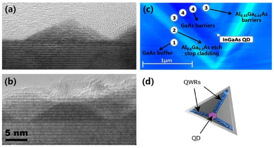
Figure 5.
(a,b) Pyramidal GaN QDs with 12 ML and truncated pyramidal GaN QDs with 8 ML [111]. (c) AFM image of a pyramidal InGaAs QD scanned in cross-section [112]. (d) A pyramidal InGaAsN QD is connected with lateral quantum wires (QWRs), among which the distribution of N atoms is depicted by white dots [113].
2.1.4. Structure and Growth of Pyramidal II–VI Quantum Dots
In the semiconducting QD family, II–VI semiconductors encompass the entire visible and near-ultraviolet regions, with large electric-optical coefficients, high exciton binding energies, and high light saturation intensities [114]. Accordingly, these materials are expected to be widely utilized in semiconductor QD lasers, photodetectors, and other fields. However, the structures of II–VI semiconductor QDs are unstable and prone to Ostwald ripening. To address this issue, Suemune et al. prepared a highly stable CdS/ZnS truncated PSQD (GaAs(001) substrate) in which CdS was epitaxially grown laterally on the (001) plane and {034} facets of ZnS [115]. Scheerschmidt et al. synthesized truncated pyramidal CdSe/ZnSe QDs on a GaAs(001) substrate, which include {011}, {112}, {113}, and {136} facets. Furthermore, the formation of this shape is relevant to the low CdSe content at the tips of the pyramids and the high level of strain around the islands [116].
2.1.5. Structure and Growth of Pyramidal IV–VI Quantum Dots
The IV–VI semiconductor QDs have been extensively applied in optoelectronic devices, and common IV–VI semiconductor QDs mainly include PbSe and PbS [117]. Although PbSe has been reported as a narrow band gap semiconductor (0.27 eV) with broad application prospects in the fields of photoelectronics and thermoelectrics, it has recently been discovered that the Auger recombination mechanisms are anomalous in this system [118,119]. In addition, Abtin et al. prepared pyramidal PbSe QDs and observed that they are prone to overgrowth [120]. As the anion surface exchange reaction induces a significant shape change (rounded shape), resulting in a significant reduction in height, the pyramidal structure of the PbSe QDs must be preserved in the barrier layer. Preobrajenski et al. synthesized pyramidal PbS QDs on an InP(110) substrate [121]. The base of each pyramidal PbS QD is formed by the (14) face and the largest facet is formed by the (001) face, and the appearance of this shape may be related to the difference in the free surface energy (or surface tension) of these systems.
2.1.6. Preparation Methodology of Pyramidal Semiconductor Quantum Dots
From the above observations, it is clear that the growth morphologies of PSQDs and truncated PSQDs are related to many effects involving both internal and external factors. In terms of the internal factors, PSQDs exist in a metastable thermodynamic state and are prone to phase transitions by virtue of the different growth rates of the various crystal planes. Moreover, a greater capillary effect is conducive to enriching atoms and generating crystal planes with larger curvatures. In terms of the external factors, the temperature, substrate components, and synthetic processes are known to impact the atomic diffusion rate and the resulting crystal quality. Currently, the most remarkable method for the preparation of PSQDs is the chemical vapor deposition (CVD) technique [122]. Unlike the solvothermal and sol–gel methods, no surfactants are present on the surfaces of nanomaterials prepared by CVD. In addition, owing to the higher preparation temperature, the obtained materials exhibit a superior crystallinity, which is conducive to the preparation of nanomaterial devices.
Due to the fact that the zero-dimensional nanomaterials prepared by CVD are not anisotropic, it is not necessary to control their epitaxial growth. Therefore, the kinetic process involved in the preparation of nanomaterials using the CVD approach is relatively simple, and the resulting particle size is uniform. At present, the majority of PSQDs are synthesized using the metal–organic chemical vapor deposition (MOCVD) technique. This technique is based on vapor-phase epitaxial growth and exploits the volatility of metal–organic compounds for metal transport [123]. Since patterned template-assisted methods are commonly used to prepare PSQDs, the MOCVD method is relatively mature and is suitable for the large-scale preparation of PSQDs with good crystallinity and uniform size. For a detailed discussion of the MOCVD method, the reader may refer to two classical reviews by Kapon and Pelucchi et al. [124,125]. In addition to the MOCVD approach, molecular beam epitaxy (MBE) has also been developed for the preparation of PSQDs with simple structures [126]. These semiconductor QDs can easily and spontaneously form a pyramidal structure under vapor phase deposition conditions, and so the PSQDs synthesized via this method do not require template assistance. Compared to MOCVD, the MBE growth rate is reduced, and the growth temperature is relatively low. Accordingly, high precision growth control can be achieved to accurately control a range of characteristics at a single molecular (atomic) scale, including the film thickness, components, and doping concentration [127]. Furthermore, MBE utilizes an ultra-high vacuum environment (1 × 10⁻¹⁰ Torr) and high-purity source materials (6–8 N), thereby leading to the generation of highly pure products. However, MBE requires a long epitaxial growth time, is not suitable for mass production, and has high requirements for the employed vacuum conditions. As a result, optimization of this approach remains an ongoing priority. In this context, a technique known as droplet epitaxy has been developed for implementation with MBE [128]. Droplet epitaxy can be used to prepare novel low-dimensional semiconductor structures, such as low-density quantum rings, QDs, and QD pairs (QD molecules) [129,130,131]. For example, Watanabe et al. prepared high-quality pyramidal GaAs/AlGaAs QDs using a modified droplet epitaxial technique, indicating its broad application prospects in the preparation of PSQDs [132]. The preparation methods of different PSQDs are shown in Table 2.
Table 2.
Some PSQDs with different preparation methods.
2.2. Pyramidal Semiconductor Nanorods (Nanowires) with Different Components
2.2.1. Structure and Growth of Pyramidal II–VI Nanorods (Nanowires)
PSNRs have received much research attention, with the most commonly used PSNR material being ZnO [133]. ZnO is a typical example of a II–VI wide band gap semiconductor and has important application prospects in ultraviolet optoelectronic devices [134,135,136]. Compared with ZnSe, which is also a II–VI semiconductor material, ZnO possesses a superior material quality; however, the application of ZnO devices still faces great technical difficulties. Among them, the p-type doping of high-quality ZnO is challenging, thereby restricting the further development of ZnO semiconductors [137]. Since the growth orientation of nanomaterials is determined by the surface energy, the shape complies with the principle of minimum total surface energy [138]. In the case of ZnO nanocrystals, the main equilibrium morphologies are cylindrical and hexagonal prisms; any deviation from these equilibrium morphologies can easily increase the systemic Gibbs free energy [139,140]. As a result, compared with the equilibrium morphologies of ZnO nanomaterials, the specific surface free energies of one-dimensional pyramidal ZnO NRs are higher, and the spontaneous formation of PSNRs is challenging. To address this issue, McPeak et al. used a continuous-flow microreactor to prepare one-dimensional truncated pyramidal ZnO NR arrays on a heated glass/silicon substrate [141]. As shown in Figure 6a, these truncated pyramidal ZnO NRs possess three crystal planes with different orientations, including the (0001), (101), and (100) planes. Notably, unlike the ZnO hexagonal prism, the truncated pyramidal ZnO NRs contain a (101) plane. This can be attributed to the higher growth rate of ZnO on the (0001) plane than that on the (101) plane under the conditions of a higher reactant concentration and a high flow rate. Thus, the geometric shape of the (101) plane is retained when the truncated pyramidal ZnO NRs complete the ripening process. In another study, Tharsika et al. successfully prepared pyramidal ZnO NRs on a glass substrate using zinc acetate and tin chloride pentahydrate as precursors [142]. However, in contrast to the system reported by McPeak et al. [141], no (0001) plane was detected at the tip of the ZnO NRs (Figure 6b,c). This was due to the presence of Sn4+ ions in the seed layer (Zn2+/Sn4+ molar ratio = 3:1), which in turn led to a fast relative growth rate of the (0001) plane, which eventually disappeared. Notably, the controllable preparation of pyramidal ZnO NRs was also achieved by the doping of specific transition metal elements. For example, Patra et al. prepared Co-doped pyramidal ZnO NR arrays on a polycrystalline glass substrate [143]. They discovered that although the ZnO NRs still grew along the crystallographic orientation of the c-axis, the presence of Co ions inhibited the NR growth rate on some specific crystal planes. As a result, the tips of the ZnO NRs retained their pyramidal shapes. In another study, Kim et al. prepared Ga-doped ZnO NR arrays with pyramidal tips on a c-plane sapphire substrate [144]. However, they found that the pyramidal ZnO NRs possessed a high stacking fault density owing to the presence of the Ga dopant.
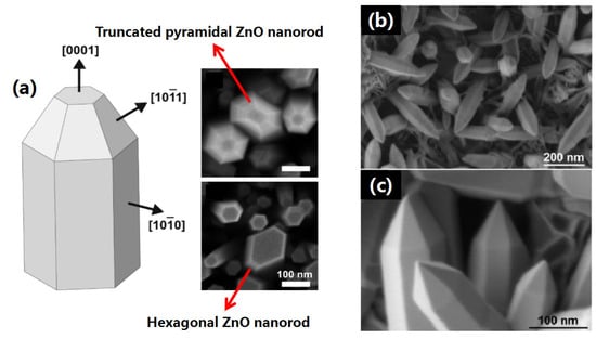
Figure 6.
Different growth morphologies of the ZnO nanorod: (a) truncated pyramidal and hexagonal ZnO nanorods [141]. (b,c) Pyramidal ZnO nanorods [142].
In addition to ZnO, the growth and preparation of pyramidal ZnTe NRs have also attracted considerable research attention. ZnTe is a p-type wide band gap semiconductor material (free hole concentration ≤1020 cm−3) with a band gap of 2.26 eV at room temperature. Similar to other II–VI semiconductors, ZnTe also possesses great potential for application in the field of optoelectronics [145,146]. However, the n-type doping of ZnTe is particularly challenging due to defect compensation during crystal growth, the low uncompensated solubility of intentionally doped impurities, and the high activation energies of some known donor or acceptor levels [147]. In the context of this material, Fonseca et al. prepared Au-catalyzed ZnTe NRs on a ZnTe(111)B substrate, wherein the ZnTe NR morphology could be controlled by varying Te/Zn flux ratio employed in the reaction [148]. More specifically, at a Te/Zn flux ratio of 1.7:1, the ZnTe NR morphology was conical with a zinc-blende structure, whereas a flux ratio of 1:1 led to a cylindrical morphology with a wurtzite structure (Figure 7). In addition, Fonseca et al. found that conical ZnTe NRs grew along the [−1−1−1] plane, whereas cylindrical ZnTe NRs grew along the [000−2] plane. Consequently, it was clear that increasing the Te/Zn flux ratio led to a decreased atom diffusion length on the side walls of the NRs, ultimately influencing the morphology of the ZnTe NR product.
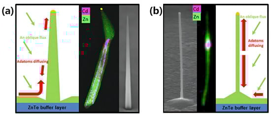
Figure 7.
Different morphologies of a ZnTe nanorod [148]: (a) cone and (b) cylindrical morphologies.
2.2.2. Other Pyramidal Semiconductor Nanorods (Nanowires)
In the study into the fabrication of pyramidal GaN NR arrays on a polar Ga template, Khan et al. found that the lateral growth rate of the pyramidal GaN NRs was faster than that of the hexagonal GaN NRs [149]. They also reported that smooth tips were obtained on N-polar templates under the same reaction conditions, and a faster lateral growth rate readily enabled the polymerization of the GaN NRs. Nano-TiO2 is a wide band gap n-type semiconductor with two main crystalline forms, namely the anatase and rutile forms, wherein the rutile form is more stable and has a denser structure [150,151]. As described in various reports, nano-TiO2 is expected to play an important role in photocatalysis, solar-energy conversion, sensing, and optoelectronic devices [152,153,154,155]. Thus, Xu et al. prepared TiO2 nanomaterials with two different pyramidal morphologies using H-titanate nanotubes [156]. They found that at pH levels ≥ 1.0, the H-titanate nanotubes initially transformed into tiny anatase nanocrystals, which continued to grow into rhombohedral anatase nanoparticles. In contrast, at pH levels ≤ 0.5, the H-titanate nanotubes initially formed hydrated titanium dioxide nanocrystals {TiO(OH2)}, and following the subsequent protonation of Ti-OH, rutile NRs with two pyramids were generated with (001), (110), and (111) orientations. Another well-known n-type semiconductor is the transparent In2O3, which possesses a wide band gap, high catalytic activity, and low resistivity. As a result, this functional material has been widely applied in optoelectronics, gas sensors, and catalysts [157,158,159]. For example, Hsin et al. fabricated pyramidal In2O3 NRs on SiO2 substrates, wherein the pyramidal tips were composed of {100} and {111} planes [160]. This result is consistent with the trend of a low total surface energy at 900 °C.
2.2.3. Preparation Methodology of Pyramidal Semiconductor Nanorods (Nanowires)
From the studies discussed above, it is clear that the growth morphologies of PSNRs are generally related to the reactant concentration, the doped ions, and the synthetic method employed. More specifically, the concentrations of the reactants and the doped ions can inhibit the growth of certain crystal planes, while different synthetic approaches can yield PSNRs with varying morphologies. For example, pyramidal GaN NRs are typically prepared using the MBE method. Due to the high melting point and high saturated vapor pressure of GaN, it cannot naturally exist in the single form, and as a result, it is difficult to prepare GaN films using the general bulk single-crystal growth method [161]. Similarly, the preparation of GaN NRs under liquid-phase conditions is challenging, often leading to their fabrication via vapor-phase deposition [149]. In contrast to the more stringent growth conditions required for GaN, the preparation of ZnTe can be achieved using both the gas- and liquid-phase approaches, although the morphology of nanoscale ZnTe prepared via the liquid-phase route is difficult to control [162,163]. Accordingly, controlling the reaction conditions using the MBE method remains the most effective method for regulating the growth morphologies of pyramidal ZnTe NRs [148]. Notably, pyramidal ZnO NRs have been successfully prepared using both gas- and liquid-phase approaches. However, magnetron sputtering is currently the preferred method for fabricating pyramidal ZnO NRs via physical vapor deposition (PVD) [144]. As presented in Figure 8a, the principle of magnetron sputtering is that, under vacuum or low-pressure gas discharge, the material source is evaporated (sputtered) into gaseous atoms (molecules) so that a new solid material coating with properties different from the substrate material is formed on the surface of the substrate [164]. However, compared with the ZnO NRs prepared using the liquid-phase approach, those obtained via vapor-phase deposition have a lower distribution density and greater numbers of defects; therefore, the liquid-phase method is often used when synthesizing pyramidal ZnO NRs [165,166]. This liquid-phase approach involves preparing a solution containing one or more suitable soluble salts, which are determined according to the stoichiometric ratio of the material composition to ensure that each element is in an ionic or molecular state [167]. During the relevant chemical reactions taking place in the solution state, the corresponding ions or molecules are uniformly precipitated or undergo nucleation crystallization to yield different types of low-dimensional nanomaterials. This method allows control of the crystal nucleation and growth of materials by adjusting the reaction conditions, including the temperature, concentration, and time, to obtain low-dimensional nanomaterials with a range of structural features. Indeed, semiconductor QDs are generally synthesized via self-assembly under liquid-phase conditions, and the resulting structures tend to be ordinarily spherical or quasi-spherical [168]. However, the edge curvature of the pyramidal QD structure is large, resulting in a high surface energy, and rendering its spontaneous formation challenging in the liquid phase. As such, the vapor-phase deposition method is commonly employed for the preparation.
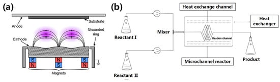
Figure 8.
(a) Schematic representation of magnetron sputtering [164]. (b) Schematic representation of a microfluidic reactor [169].
In the context of ZnO, pyramidal NRs have been prepared using a mature liquid-phase approach, which includes chemical bath deposition (CBD) and electrochemical deposition (ECD). CBD is conducive to a more effective entry of doped ions into the ZnO lattice, and it can be utilized in combination with continuous-flow microreactors, which have significantly advanced in recent years to allow the preparation of low-dimensional nanomaterials [143,169]. More specifically, a continuous-flow microreactor has been used to combine reactant mixing with the actual reaction, both of which take place in the small channels of the reactor to control the product quality. Importantly, this approach can also achieve the industrial production of nanomaterials by simultaneous parallel reactions in multiple reactors (Figure 8b). However, when preparing pyramidal ZnO NRs, it is desirable to realize nucleation at the bottom of the pore prior to a gradual upward growth to ensure that the ZnO NRs in each pore grow into a complete single crystal [141]. Thus, if the reactor pores are too slender, they are not conducive to the migration of the solute raw material for NR growth, and the pore wall may also become nucleation sites. Moreover, the resulting pyramidal ZnO NRs may possess many defects or be polycrystalline in nature. It is therefore necessary to reduce the number of defects in ZnO NRs to obtain high-purity single crystals.
With regards to the ECD method mentioned above, this is a coating technology based on the migration of current through the positive and negative ions present in an electrolyte solution, thereby promoting a range of redox reactions in the electrode under the action of an external electric field (Figure 9a) [170]. In the context of nanomaterial preparation, the ECD method offers the advantages of good orientation and fewer defects; therefore, it is favored by researchers. In addition, ECD can achieve nanomaterial growth under low-temperature and high-current density conditions, which accelerates the growth rate and results in a more uniform particle size. Importantly, using the ECD approach, ZnO NRs with different morphologies can be prepared by adjusting the process parameters, including the current intensity, reaction time, and reaction temperature [171]. In this context, Alimanesh et al. prepared ZnO NR arrays with pyramidal shapes and hexagonal prisms on an n-type Si(100) substrate using ECD, during which they controlled the reaction conditions to obtain these different morphologies [172]. Spray pyrolysis, which also employs a liquid-phase solution as the precursor, has also been reported for the preparation of pyramidal ZnO NRs [142]. In this case, under high temperature and vacuum conditions, nano-powders with smaller particle sizes and improved dispersions can be obtained. It is therefore clear that the spray pyrolysis approach exhibits a number of advantages over both the gas- and liquid-phase methods (Figure 9b) [173]. The preparation of some pyramidal NRs can also be achieved by adjusting the pH of the reaction solution, and the synthesis of pyramidal TiO2 NRs is a simple example [146]. As mentioned above, variation in the pH value can lead to the generation of nano-TiO2 species with different pyramidal shapes. Taking advantage of this approach, Zeng et al. prepared pyramidal ZnO NRs with diameters of <50 nm and aspect ratios of 30–40 by the addition of a surfactant (ethylenediamine) under alkaline conditions. Notably, the presence of an alkaline environment is beneficial for the surfactant to inhibit the growth of ZnO NRs at the tip [174].
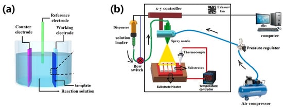
Figure 9.
(a) Preparation of nanomaterials via electrochemical deposition (ECD) [170]. (b) Schematic representation of the spray pyrolysis method [173].
3. Energy Band Structures and Electronic Properties of Pyramidal Low-Dimensional Semiconductors
3.1. Definition of the k·p Perturbation Method
Currently, research into the band structures and electronic properties of pyramidal low-dimensional semiconductors has mainly focused on narrow band gap PSQDs. For narrow band gap semiconductors, the k·p perturbation method is usually exploited to obtain the band structures. This method applies the perturbation theory and combines the requirements of crystal symmetry to study the wave function, which obtains the band structure near special symmetry points in the k space. This method uses finite parameters obtained from experiments to determine the uncertain coefficients in the band structure formula to ascertain the structural expression of the band [175]. More specifically, this method assumes that all states of Un = (0, r) (potential function) and the energy En(0) of the crystal electrons at k = 0 are known, and as a result, the expression and wave function of En(k) near k = 0 are obtained using the perturbation method according to the crystal symmetry. The band structures of special points in the k space can be determined by the band parameters, such as the band gap width, the electron effective mass, and the hole effective mass obtained experimentally, so the band structures of other points in the k space can be determined according to the k·p perturbation method [176]. Owing to the narrow band gap width, strong electron interactions, and strong electron spin–orbit interactions, these effects can be handled well by the perturbation method (Figure 10). Hence, the k·p perturbation is particularly important for narrow band gap semiconductors, as will be discussed in the following subsections.
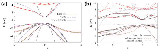
Figure 10.
Calculation of the electronic band structure using the k·p perturbation method with bulk GaAs as an example [176]: (a) zinc-blende (ZB), (b) wurtzite (WZ).
3.2. III–V Pyramidal Semiconductor Quantum Dots
Grundmann et al. studied the electronic structures of pyramidal InAs/GaAs QDs on a base length of 12 nm [177]. By studying the ground state electron wave function in the (010) or (100) cross-section, it was discovered that 70% of the probability value of the wave function was almost entirely inside the QD. Furthermore, the application of strain was found to easily shift the energy band of the pyramidal InAs/GaAs QD heterostructure. Compared with the average valence band in the absence of strain, the shift rate reached 85%, and the ground state of the hole was squeezed at the bottom of the QD owing to the existence of the strain-induced potential. However, as the lattice mismatch of InAs/GaAs reached 7%, the effective mass and conduction band offset varied greatly when the strain was considered in the calculation. To date, a number of groups have conducted in-depth studies based on the work of Grundmann et al. [177]. For example, Kim et al. utilized the pseudopotential plane wave method to calculate the electronic structures of the {101}, {113}, and {105} planes and observed that the shape of the QD has an important influence on the electronic structure [178]. In addition, Cusack et al. exploited the multiband effective mass theory to calculate the energy levels and electronic wave function, which contrasts with the basic assumption that the conduction and valence bands are decoupled [179]. As a result, their calculations revealed that the energy levels of the first- and second-hole excited states were split in the valence band due to the mixing of the different bulk states.
In another study, Wang et al. used the electronic structure of the InAs/GaAs QD (110) plane to adopt an atomic model to replace the continuum model, wherein the potential was obtained by superposition of the shielded atomic pseudopotential [180]. The strain was obtained by minimizing the atomic strain energy, and the wave function was expanded using the plane wave basis set. In the field of calculating self-consistent electronic structures, Fonseca’s group applied the effective mass approximation and localized spin density approximation to correct the calculation error of the electronic structure for pyramidal InAs/GaAs QD induced by noncompliance with Hund’s rule [181]. Recently, Klenovsky et al. discovered that the electronic structures of truncated pyramidal (InGa)(AsSb)/GaAs/GaP QDs exhibit concurrently direct and indirect transitions in both real and momentum space [182]. Therefore, such QDs have potential value for application in quantum information technology compared with (In,Ga)As/GaAs QDs. Figure 11 shows the electronic structures of (InGa)(AsSb)/GaAs/GaP QDs.
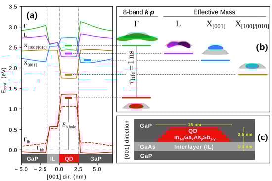
Figure 11.
The electronic states of (InGa)(AsSb)/GaAs/GaP QDs [182]: (a) the confinement potentials. (b) Electron and hole probability densities. (c) The structure of truncated pyramidal QD in [001] direction.
Considering the band structures of III-V PSQDs, the physical properties of the QDs can be effectively improved through doping. For example, in the case of pyramidal (In,Ga)As/GaAs QDs, the band structure was calculated by Stoleru et al. using the eight-band strain-dependent k·p perturbation method, and it was found that the band gap of the QD increased significantly due to the large hydrostatic pressure [183]. In addition, Califano et al. used the eight-band k·p perturbation method to study the band order and the conduction band effective mass of pyramidal In1−xGaxAs/GaAs QDs and SixGe1−x/Si QDs [184]. However, when studying the valence band effective mass, the valence band states Γ7 and Γ8 cannot be treated in the original method by virtue of their uncoupling with one another. With this in mind, Califano et al. developed the 14-band k·p perturbation method to obtain the non-zero matrix elements that appear in the band calculations. In another study, Lee et al. provided an alternative calculation method for solving the energy band of pyramidal InAs/GaAs QDs [185]. More specifically, they sandwiched a symmetric square pyramidal QD between two conical quantum dots to ensure that the ground-state energy of the square pyramidal QD was the average of the ground-state energies of the two conical QDs. As a result, the obtained error was within 1% of the results compared with Califano et al. [184]. Furthermore, Kapon et al. introduced vertical AlGaAs quantum wires between pyramidal GaAs/AlGaAs QDs, which acted as channels for the capture of excited electrons [186]. It was also found that the perpendicular quantum wire barrier simultaneously expanded the energy separation between the s- and p-states, whilst reducing the sensitivity of the s-state energy to size fluctuations. The electron states of pyramidal GaAs/AlGaAs QDs connected with vertical AlGaAs quantum wires are shown in Figure 12.
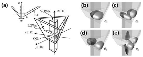
Figure 12.
Model of the electron states in a pyramidal quantum-dot heterostructure [186]: (a) a definition of the geometrical parameters, among which VQWR and LQWs denote that vertical quantum wire and lateral quantum wells, respectively. (b) The s-like (e1) ground state. (c,d) The p-like (e2) doubly degenerated first excited states. (e) The second excited state.
Nakaoka et al. utilized an eight-band effective mass model to calculate the band structures of InAs and InGaAs QDs under an external magnetic field [187]. Their calculations predicted that the absolute value of the conduction band and valence band g factor (i.e., the coefficient connecting the spin moment and magnetic moment) increases with an increase in the QD size, which is conducive to future quantum information processing. Additionally, during the calculation of the band structures of zinc-blende semiconductor QDs, Tomic et al. proposed a calculation method for InAs/GaAs QDs and InGaAsN QDs, which was based on parallel multi-band k·p program instructions [188]. In the plane wave method, the strain tensor elements given in a semi-analytical form are irrelevant and can provide effective parallel processing when setting a complete Hamiltonian matrix for direct diagonalization. Consequently, when this method is used to calculate complex QD structures, it can be regarded as a linear combination of the Fourier transforms of several simple characteristic shapes (box, cylinder, and cone), thereby constituting a continuation of the work carried out by Lee et al. [185].
A core–shell structure is obtained by growing one or more layers of nanomaterials on a seed. The most typical example is the synthesis of core–shell and core–shell–shell QDs reported by Alivisatos et al. [189,190,191], wherein such structures with different compositions and sizes can be epitaxially grown using a range of experimental methods. In one example study of pyramidal core–shell QDs, Osorio et al. studied core–shell QDs consisting of a GaAs core embedded in an AlGaAs matrix, and discovered that under the action of an external electric and magnetic field, the transitions between a large number of electronic states (transformation matrix elements) may be prohibited, while the presence of external probes and related degenerate destruction can activate some of these transitions [192]. Figure 13 shows the electron states of pyramidal core–shell AlGaAs/GaAs quantum dots, among which the external electric and magnetic field is applied along the z-direction. It has also been found that the interactions between these transitions can have an important influence on the energy levels of individual QDs. For example, Jaskolski et al. studied two vertically stacked pyramidal self-assembled InAs/GaAs QDs using an empirical tight-binding approach and observed that even if multiple atomic layers were separated between the two QDs, they still had a strong coupling effect [193]. However, when the separation distance was reduced to 3 ML, the splitting of the electron and hole energy levels was comparable to the energy-level spacing of an individual pyramidal QD, and the energy levels could cross.
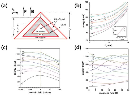
Figure 13.
Electron states of the core–shell AlGaAs/GaAs quantum dots [192]: (a) structural diagram of the pyramidal core–shell quantum dot. (b) Energy of the lowest thirteen confined electron states (1–13) in a GaAs–Ga0.7Al0.3As pyramidal core-shell quantum dot as functions of the innermost height (h1). Calculations correspond to F = 0, B = 0, θ = π/2, h2 = 20 nm, and h3 = 30 nm. The inset shows the energies of the three lowest confined states when h1 approaches h2. (c) Energies of the lowest thirteen bounded states (1–13) for an electron confined in a GaAs-Ga0.7Al0.3As pyramidal core–shell quantum dot as a function of the applied electric field (F). Calculations correspond to B = 0, θ = π/2, h1 = 5 nm, h2 = 20 nm, and h3 = 30 nm. (d) Energies for the first thirteen confined electron states (1–13) in a GaAs-Ga0.7Al0.3As pyramidal core–shell quantum dot as a function of the applied magnetic field (B). Calculations correspond to F = 0, θ = π/2, h1 = 5 nm, h2 = 20 nm, and h3 = 30 nm.
In terms of the influences of external factors on the band structures of III-V PSQDs, it should be noted that the majority of energy band calculations of InAs/GaAs QDs do not consider the wetting layer. Thus, using an effective electron Hamiltonian (electron effective mass approximation depending on the energy and position), Markiewicz et al. studied the electronic structure of InAs/GaAs QDs containing a wetting layer and found that the existence of the wetting layer fundamentally affected the electronic structure [194]. This result implies that the eigenvalues in the presence of a wetting layer are substantially smaller than those in the absence of a wetting layer. Typically, InAs/GaAs QDs are encapsulated to prevent their oxidation. However, during their investigations into the electronic structures of uncapped pyramidal InAs/GaAs QDs, Saito et al. exploited tight-binding analysis to study the strain energy distribution and electronic structure of the QDs and found that the internal atoms at the bottom of the QD exhibit the largest degrees of strain, while the atomic layers near the top of the pyramid exhibit almost no strain [195]. This strain distribution results in a large energy gap (1.74–2.71 eV) due to the strong confinement effect in the internal electronic states. In another study, Williamson et al. investigated InAs QDs with independent structures [196]. They compared the electronic structures of independent spherical InAs QDs with those of pyramidal InAs QDs embedded in a GaAs substrate and demonstrated that the energy band of the independent InAs QDs exhibited a large degree of discontinuity.
The electronic properties of truncated pyramidal InAs/GaAs QDs have also been examined, with pioneering work by Pryor et al. dominating this area [197]. This group employed the strain-dependent eight-band k·p Hamiltonian operator to calculate the energy bands of truncated pyramidal InAs/GaAs QDs and observed that the energy of the electron-confined state of the QDs with 101-type planes is closely related to the bottom of the pyramid, but not highly sensitive to the height. More specifically, the conduction-band ground state changes by 250 meV with the increase in base length (5.5–20.5 nm), whereas different values of height only give energies with 5 meV of each other. The valence-band states alter by 150 meV when the base length is varied, while changing height alters the energy by ≤10 meV.
In addition to III-V PSQDs, researchers have also studied III-V pyramidal semiconductor clusters, which are relatively stable microscopic or sub-microscopic aggregates composed of dozens or even thousands of atoms, molecules, or ions bonded through physical or chemical forces. The physicochemical properties of these materials are known to be transformed upon variation in the number of contained atoms [198,199,200]. Due to the fact that clusters embrace the initial state of condensed matter and the transition states of various substances from atoms and molecules to bulk substances, they can be regarded as a new level of material structure between atoms, molecules, and macroscopic solid substances. With this in mind, Pozhar et al. applied the multi-configuration self-consistent field approximation method to study the electronic properties of pyramidal Ga10As4 and In10As4 clusters [201]. In the space outside the vacuum cluster, the charge density distribution decreased more rapidly, and the falling rate of the In-based vacuum clusters was twice as slow as that of the Ga-based vacuum clusters.
Upon the application of an external electric field to the QDs, a quantum-confined Stark effect occurs, in which the energy band of the QDs tilts (Figure 14), resulting in a decrease in the effective band gap and a red-shift in the absorption edge [202]. Fry et al. were the first group to study the Stark effect of truncated pyramidal InAs/GaAs QDs, and they observed that, under the action of an external electric field, the holes were located above the electrons and were confined to the tips of the QDs [203]. For example, in the case of InAs QDs with a GaxIn1−xAs gradient composition wherein x gradually decreases from the substrate to the top of the structure, this situation will occur. Based on the work of Fry et al. [203], Sheng et al. carried out an in-depth study using the eight-band strain-dependent k·p method [204]. They found that the linear dependence of the built-in electric dipole moment on the Stark shift was broken owing to the effects of the three-dimensional strain field distribution in the self-assembled QDs. However, the truncated pyramidal and slender lens-shaped self-assembled QDs exhibited a normal linear dependence of the Stark shift on the electric dipole moment, which reflects the two-dimensional characteristics of electron-hole confinement.
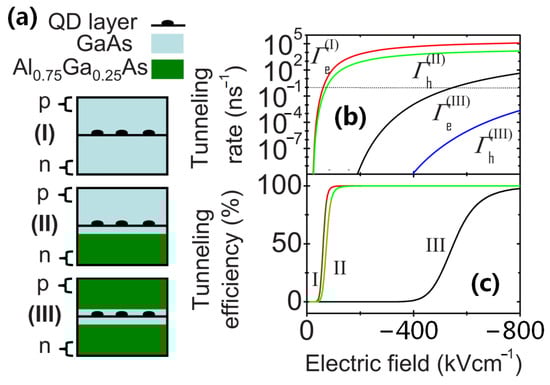
Figure 14.
Tunneling in different heterostructure designs with the Stark effect [202]: (a) device designs considered for observation of the Stark effects exhibited by single quantum dots in a vertical electric field, including I, II and III QD heterostructures; (b) tunneling rates for the electrons (I and III QD heterostructures) and holes (II and III QD heterostructures) in the designs presented in part (a); and (c) the proportion of carriers that tunnel out of a state with a fixed 1 ns lifetime state.
In another study, Jin et al. quantitatively investigated the Stark effect in self-assembled InAs/GaAs QDs, and discovered that the quantum-confined Stark shift of the ground-state inter-band transition was ~34 meV when the electric field intensity was increased from 105 to 308 kV/cm [205]. In addition, Wang et al. studied the quantum-confined Stark effect in interdiffusion semiconductor QDs and found that three-dimensional isotropic In-Ga interdiffusion plays a key role in determining the quantum transition energy of the pyramidal InAs/GaAs QD structure under the action of an external electric field [206]. Wang et al. also discovered that a non-zero built-in dipole moment exists in pyramidal QDs, whereas uniform Fick interdiffusion significantly reduces the built-in dipole moment to enhance the Stark shift. Moreover, Troncale et al. utilized the Stark effect of quantum confinement to study the hole characteristics and dynamic conversion of the single-photon polarization state in the dot-in-dots (DiDs) of pyramidal GaAs/AlGaAs QDs [207]. They found that the asymmetric DiD structure is particularly suitable for the conversion effect under a medium-intensity electric field (<kV cm−1), which is conducive to polarization control at the single-photon level.
3.3. III-Nitride Pyramidal Semiconductor Quantum Dots
For III-nitride semiconductors with wide band gaps, the electron spin–orbit interaction is weak owing to the large band gap energy. Therefore, when using the k·p method to calculate the band structure, the formula can be approximated [208]. Taking the truncated pyramidal GaN/AlN QDs as an example, Andreev et al. developed a plane wave expansion method using the multi-band k·p model to calculate the spectra of the carriers and the wave functions of the QDs [209]. However, the spin–orbit separation energy of wurtzite GaN and AlN is extremely small (i.e., 5–10 meV), and so the influence of the spin–orbit energy can be ignored when calculating the Hamiltonian of the energy band. In addition, it was discovered that the electron wave function of small QDs (height = 1.8 nm) is primarily concentrated in the centers of the QDs, while the hole wave function is principally concentrated in the wetting layer. The electron wave function of the large QDs (height = 3.6 nm) is generally concentrated at the tips of the QDs, while the hole wave function is concentrated in the wetting layer (Figure 15). Accordingly, with an increase in the QD size, the radiation lifetime also increases rapidly.
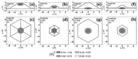
Figure 15.
The probability density distribution (|Ψ|2) of truncated pyramidal GaN/AlN quantum dots [209]: (a,c) The electron wave function of a large quantum dot; (b,d) the electron wave function of a small quantum dot; (e,g) the hole wave function of a large quantum dot; and (f,h) the hole wave function of a small quantum dot.
In this context, Marquardt et al. studied the energy bands of truncated pyramidal GaN/AlN QDs, comparing the differences between the multi-band k·p model, the effective bond orbit method, and the empirical tight-binding model for calculation of the electronic structure [210]. It was found that although the band gaps of GaN and AlN are large, the electronic binding energy calculated by the eight-band k·p model deviates greatly from the results calculated by the decoupled 6 + 2-band k·p model (the electron effective mass method). This can be attributed to the fact that for a wide band gap, the influence of the Kane matrix parameter Ep cannot be ignored in the calculation results. On the other hand, although the eliminated spin–orbit parameters enhance the degeneracy of the first two holes, and the spin–orbit separation parameters of GaN and AlN are much smaller than that of CdSe (0.4 eV), the splitting energy levels generated by these species possess the same order of magnitude. Therefore, it is not appropriate to ignore the spin–orbit parameters in the case of GaN/AlN QDs, which corrects the work of Andreev et al. [209].
3.4. II–VI Pyramidal Semiconductor Quantum Dots
During their work on the energy band structures and electronic properties of pyramidal II–VI semiconductor QDs, Hong et al. focused on self-assembled pyramidal CdTe/ZnTe QDs, analyzing the influence of the strain field on the energies of the conduction band and the valence sub-band using the eight-band k·p Luttinger–Kohn Hamiltonian [211]. They found that in terms of the mechanical properties, in contrast to InAs/GaAs QDs, the strain of the CdTe/ZnTe QDs changes constantly through the wetting layer due to the different material parameters. In addition, with regards to the energy band properties, owing to the higher height of the strain-induced potential of the conduction sub-band, the valence sub-band (hole) wave function was more strongly confined to the QDs than the conduction sub-band (electron) wave function. Upon increasing the thickness of the CdTe wetting layer, the energy of the conduction band and the valence sub-band decreased due to the greater width between the two confined potentials induced by the strain field. Furthermore, although an increased wetting layer thickness causes diffusion of the strain field into the substrate and the capping layer, the valence sub-band and the band-edge energy of the conduction band move upward simultaneously. Moreover, Hong et al. compared the calculated values of the energy band with experimental data and discovered that the thickness of the wetting layer significantly changes the conduction band edge but has little impact on the heavy-hole band edge [211]. In another study, Seoung et al. investigated the Stark effect in pyramidal CdTe/ZnTe QDs using the eight-band strain-dependent k·p model [212]. Upon the application of an external electric field along the QD growth direction, they found that the transition energy underwent a red-shift. However, when the applied direction of the external electric field was opposite to the growth direction, the redshift in the transition energy decreased slightly.
3.5. Summary
To date, researchers have studied the energy band structures and electronic properties of III–V PSQDs, and the conclusions drawn from these investigations have been extremely rich, especially in the case of pyramidal InAs/GaAs QDs. More specifically, it has become clear that these features are affected by both internal (structure and composition) and external (wetting layer, electric field, and magnetic field) factors [177,178,179,180,181,193,194,195,196,197]. However, when using the multi-band k·p model to study pyramidal QDs, a number of difficulties have been identified, including the effectiveness of the method being limited to the center of the Brillouin zone and the fact that the Bloch function is not affected by the material and strain alteration. Moreover, for the envelope function across the heterogeneous interface, it has also been revealed that the selection of the appropriate boundary conditions and the relevant matching criteria is challenging. Consequently, in recent years, with the increasing refinement of research into the energy band structures of nanomaterials [213,214,215,216,217,218], the finite element simulation method has been exploited to study PSQDs in the context of computational material physics, thereby simplifying the calculation of the energy band and producing highly accurate carrier ground-state energy values.
4. Fundamental Optical Processes Based on Pyramidal Low-Dimensional Semiconductors
The intrinsic absorption properties of semiconductors are known to correspond to the physical process in which valence-band electrons absorb photons and are injected into the conduction band. The spectra of semiconductors are located over the ultraviolet to near-infrared light regions, which have high absorption coefficients. The absorption over this region coincides with the intra-band transition of electrons within the conduction band or holes within the valence band, which is also known as free-carrier absorption. In the low-energy region of the absorption spectrum, peaks associated with the lattice vibration absorption can be found, as well as peaks related to the impurity electronic state transition. In contrast, the photoexcitation process is inseparable from the participation of excitons [219,220]. The exciton is regarded as an elementary excitation that can transport energy without transporting net electric charge, and as such, it is classed as a Coulomb-correlated electron-hole pair. After absorbing a photon, the electron is excited to the conduction band, and a hole is formed in the valence band, which may rebound to generate an exciton by virtue of the Coulombic attraction between the electron and hole (Figure 16) [221]. Considering the important role of excitons in optoelectronics, the excitonic behavior related to PSQDs is now considered.
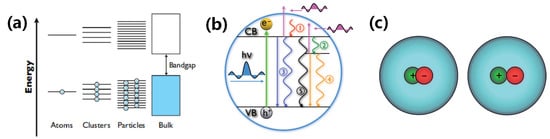
Figure 16.
Exciton dynamics in semiconductor nanocrystals [221]: (a) illustration of the quantum confinement effect in different systems ranging from atoms to clusters to particles and finally to bulk materials; (b) illustration of key dynamic processes in a quantum dot and in a related pump-probe transient absorption measurement. The excitation or pump is represented as a green arrow and the probe is represented as fuchsia-colored arrows. Different dynamic processes shown include the following: (1) electron relaxation through electron–phonon coupling within the conduction band following excitation across the band gap; (2) trapping of electrons/holes into trap states due to defects or surface states; (3) radiative and nonradiative band-edge electron-hole (or exciton) recombination; (4) radiative and nonradiative trapped electron-hole (or relaxed exciton) recombination; and (5) nonlinear and nonradiative exciton–exciton annihilation. (c) Schematic illustration of strongly bound (left) and weakly bound (right) excitons in a semiconductor nanocrystal.
Type I heterostructures are composed of two semiconductors with different band gaps in which one material has a higher valence band and lower conduction band than the other [222]. Moreover, type II heterostructures are composed of two semiconductors with medium band gaps (>1.3 eV) where the conduction and valence bands of one material are higher than those of the other [223]. The exciton properties of charged type II Ge/Si QDs were initially studied by Yakimov et al. using electron-filling modulation absorption spectroscopy [224]. It was discovered that compared to type I Ge/Si QDs, when exciton–hole and exciton–exciton complexes are formed in type II systems, the ground state absorption peak undergoes a blue shift, which is related to the localization effect of electrons and holes, in addition to leakage of the electron wave function in the QDs. It was also demonstrated that when two excitons are excited in a QD, the electrons are spatially separated and have different single-particle quantization energies [225].
During their investigation into pyramidal InAs/GaAs QDs, Anitha et al. employed pyramidal GaAs QDs as a model to study the exciton binding energy [226]. It was found that the non-parabolic characteristics of the conduction band will affect the light-hole and heavy-hole excitons, thereby rendering them more susceptible to binding than excitons with the parabolic characteristics of the conduction band. In addition, the same study demonstrated that the dielectric screening function can affect the light-hole and heavy-hole excitons, enabling them to become more easily constrained than excitons without the dielectric screening function. Furthermore, the spatially dependent effective mass was found to affect the light-hole and heavy-hole excitons, so that their binding degrees were lower than those recorded in the absence of a spatially dependent effective mass. Heitz et al. investigated the phonon-assisted exciton transition of self-assembled pyramidal InAs/GaAs QDs using selective excitation PL and PL excitation spectroscopy, and they observed that there is no Stokes shift between the intrinsic recombination of coherent InAs/GaAs QDs, the ground state absorption, and the emission [227]. However, in a subsequent study by Heitz et al. [228], it was discovered that there is a significant correlation between the biexciton binding energy and the exciton transition energy. Additionally, a transition from binding to anti-binding appeared at ~1.24 eV, which was attributed to a decrease in the exciton localization induced by the finite barrier height. Other works in this area included a study by Jaskolski et al. [193], who elucidated the band structure and electronic properties of double-pyramidal InAs/GaAs QDs, while Schliwa et al. studied the exciton properties of a vertically stacked coupled InAs/GaAs QD pair with the same structure [229]. It was found that when the distance between the two QDs is <17 ML, the electrons produce an immensely strong distance-dependent quantum coupling, resulting in spectral term splitting between the ground state and the first excited state (Figure 17). Accordingly, the exciton absorption spectrum is strongly related to the distance from the vertical point in terms of the energy range, order, peak shape, and polarization anisotropy.
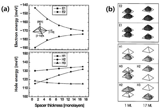
Figure 17.
Exciton properties of the vertically stacked coupled InAs/GaAs quantum dot pairs [229]: (a) electron and hole energies in the vertical quantum dot pairs with respect to the GaAs matrix band edges for varying the spacer thickness, among which E1, E2, H1, H2, and H3 denote that ground state electrons, excited electrons, ground state holes, the first excited holes, and the second excited holes, respectively. The symbols refer to states with similar wave function shapes, and the lines are guides to the eye. (b) Probability density isosurfaces (p = 65%) of the electron and hole levels.
In a study investigating the exciton properties of truncated pyramidal InAs/GaAs QDs, Pohl et al. discovered that as the height of the truncated pyramidal InAs QDs increased from 2 to 9 ML, the fine structure splitting of bright excitons changed from a negative value to >0.5 meV, and the biexciton binding energy changed from anti-binding to binding [230]. In combination with the results of k·p model calculations and analyses, they also observed that the splitting trend of the fine structure was related to the piezoelectric effect. Moreover, the binding energies of the charged and neutral excitons increased due to the correlation between the rising number of binding states and the larger QD sizes.
Considering the exciton properties of pyramidal InAs/InP QDs, Kim et al. applied pyramidal InP nano-templates to regulate the exciton g-factor of QDs and discovered that the exciton g-factor strongly depends on the height change or emission energy of the QDs [231]. This is due to the fact that for smaller QDs, the change in confinement and the possible leakage of the wave function to the barrier materials no longer have a significant influence on the hole g factor; thus, the contribution of light holes reaches saturation. However, because this mechanism may not be applicable to InAs/GaAs QDs, the exciton g factor lacks a high degree of dependence. Through further research, Gawelczyk found that the excited state energy of pyramidal InAs/InP QDs is opposite to that of the ground-state emission energy, and this atypical relationship must be considered when using optical transitions involving higher exciton states [232].
In recent years, the exciton properties of pyramidal InGaAs QDs have attracted growing research attention owing to the development of novel quantum information technologies. In this context, Dufaker et al. studied the exciton–phonon coupling effects of InGaAs/GaAs and InGaAs/AlGaAs QDs [233]. They deduced that the exciton-longitudinal optical (LO)–phonon coupling of QDs with a GaAs barrier was slightly weaker than that of QDs with an AlGaAs barrier; the linear width of the phonon recombination was also found to increase. In addition, Jarlov et al. studied the properties of biexcitons in pyramidal InGaAs/GaAs QDs, and observed that the charge separation caused by the piezoelectric field is responsible for the positive/negative crossover of the biexciton binding energy upon increasing the QD size [234]. In particular, QDs showing a disappearance of the biexciton binding energy are expected to be applicable to quantum information processing. From a theoretical perspective, Dupertuis et al. proposed a method that can predict the true degeneracy and polarization decay modes of semiconductor QD exciton complexes, which is consistent with the spectroscopic observations made for pyramidal InGaAs/AlGaAs QDs [235]. Based on the study of the complex electronic structure of truncated pyramidal (InGa)(AsSb)/GaAs/GaP QDs by Klenovsky et al. [182], Steindl et al. further discovered that such QDs exhibit a significant blueshift with increasing pumping [236].
In the context of II-VI PSQDs, Park et al. have employed the eight-band strain-dependent k·p method to study the influence of the wetting layer on the exciton binding energy of pyramidal CdTe/ZnTe QDs [237]. They found that QDs with smaller wetting layer thicknesses display greater exciton binding energies, which lead to an increased carrier confinement effect. In addition, Hong et al. investigated the optical characteristics of type II pyramidal ZnTe/ZnSe QDs and reached a number of conclusions [238]. More specifically, they described that the band bending effect in the conduction- and valence-band potential distribution principally occurs in the QDs and in the capping layer region. Furthermore, they found that the inter-band transition energy is almost independent of the thickness of the capping layer. Moreover, the sub-band energy in the valence band decreases with an increase in the pyramidal base, whereas the sub-band energy in the conduction band is essentially independent of the length of the pyramidal base.
In general, the optical properties of III–V PSQDs (mainly pyramidal InAs/GaAs QDs) are influenced by a number of factors, including the binding energy, transition energy, band structure, and phonons, while the exciton characteristics of PSQD pairs are influenced by a strong quantum coupling effect. Notably, the optical properties of II–VI PSQDs are not only related to the band structure but are also affected by the thickness of the wetting layer. Considering the applicability of pyramidal low-dimensional semiconductors in optoelectronics, the following sections examine their use in photocatalysis, photodetectors, solar cells, quantum information applications, and other fields as examples of their research applications.
5. Applications of Pyramidal Low-Dimensional Semiconductors in Optoelectronics
5.1. Photocatalysts Based on Pyramidal Low-Dimensional Semiconductors
Photocatalysis is based on the redox ability of a photocatalyst under light irradiation, and it is commonly employed in purification, synthesis, and chemical transformations (Figure 18) [239,240]. In general, photocatalysts are semiconductors, and their catalytic mechanisms can be divided into three main steps. Firstly, under the excitation of incident light at an energy larger than the semiconductor band gap, electron-hole pairs are generated. Subsequently, the electrons and holes are transported to the semiconductor surface, and finally, when the position of the conduction band edge is higher than the potential of the reduction half-reaction and the position of the valence-band edge is lower than the potential of the oxidation half-reaction, the substance adsorbed on the semiconductor surface can be catalyzed to generate new products. Figure 19 outlines some important works in this area, as detailed in the text below.
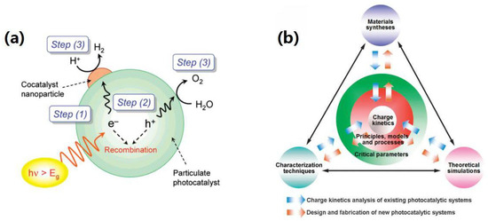
Figure 18.
The basic principle of photocatalysis: (a) processes involved in photocatalytic water splitting on a heterogeneous photocatalyst [239]; (b) schematic illustration outlining the probing charge kinetics in existing photocatalytic systems, and the steering of the kinetics based on the design and fabrication of new photocatalytic systems at the intersection between materials synthesis, characterization techniques, and theoretical simulations [240].
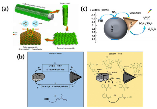
Figure 19.
A pyramidal low-dimensional semiconductor photocatalyst: (a) catalytic mechanism of a micro-pyramid on the surface of a CoO nanorod [241]; (b) photocatalytic mechanism associated with pyramidal ZnO nanomaterials [242]; and (c) schematic representation and approximate band alignment of CdSe/CdS quantum dot-sensitized TiO2 photoanodes [243].
As presented in Figure 19a, Ling et al. used surface engineering to prepare a pyramidal CoO array with a size of ~5 nm on the surface of one-dimensional single-crystal CoO NRs [241]. They discovered that these CoO NRs exhibited excellent catalytic activity and durability for the redox/oxygen evolution reaction. More specifically, the electrochemical activity was found to be derived from the presence of oxygen vacancies, which are easily generated on the oxygen-terminated {111} plane. These vacancies benefit the electronic structure of CoO to ensure rapid charge transfer and optimal adsorption performance for the intermediate products. In another study, Pinkas et al. studied the catalytic properties of ZnO nanocrystals with two different pyramidal morphologies as quantum photoinitiators (Figure 19b) and found that the catalytic performance of the truncated pyramidal NRs was superior to that exhibited by pyramidal nanocrystals in water-based and solvent-free formulations [242]. This was attributed to the overall enhancement of the photocatalytic properties of the truncated pyramidal ZnO NRs, which in turn was associated with the photoinitiation process and faster oxygen consumption. Furthermore, Zhao et al. prepared pyramidal thick-shell CdSe/CdSexS1−x/CdS QDs via a combination of thermal injection and successive ionic layer adsorption reactions (SILAR), giving a quantum yield 15% higher than that of obtained for CdSe/CdS QDs [243]. Moreover, because of the spatial separation of the electron-hole wave function, these QDs possess a long radiative lifetime of up to 100 ns, in addition to significantly broadened light absorption from 500 to 700 nm; thus, the CdSe/CdSexS1−x/CdS QDs are expected to have extremely high application value in the preparation of hydrogen from water splitting (Figure 19c).
5.2. Photodetectors Based on Pyramidal Low-Dimensional Semiconductors
A photodetector is a sensor that converts optical signals to electrical signals [244,245,246]. When excess electrons and holes are generated in a semiconductor, the conductivity of the material increases; such alternation of conductivity is the basis of photodetectors. In this process, photogenerated electrons are formed, and the electrons drift to the photoconductor anode under the action of an external electric field. To meet the principle of electrical neutrality in the photoconductor, electrons are generated at the cathode and then drift to the anode, wherein the entire drift process corresponds to the average lifetime of the excess carriers. After this time, the photoelectrons recombine with the holes. Figure 20 shows the application of photodetectors.
Figure 20.
Application of photodetectors: (a) schematic representation of an InAs photoconductor nanowire operating in the visible-to-near infrared regime [244]; and (b) schematic representation of a BP photodetector operating at 3.39 μm [245].
QD-based detectors are extensively used for infrared light detection. Theoretically, QD infrared detectors exhibit excellent performances, including a normal incidence, a low dark current, a high gain, a large detection rate, good responsiveness, and the ability to operate at room temperature [247,248,249,250]. These advantages in extending the electron lifetime are derived from the three-dimensional confinement of the carriers, which is excited by the substantially suppressed electron–phonon interactions [251,252,253,254]. Another important feature of QD infrared photodetectors is their sensitivity to vertically incident infrared radiation, which is advantageous for applications in focal-plane arrays. However, because the size inhomogeneity and stress accumulation of QDs limit the number of QD layers prepared during material growth, there is still a large gap between the performance indices of QD detectors and the theoretical expectations.
Boucaud et al. were the first group to study the mid-infrared intra-band absorption effect of pyramidal self-assembled Ge/Si QDs using light-induced absorption technology [255]. They observed that the mid-infrared absorption of the in-plane polarization reached a maximum of ~300 meV, and this was attributed to the transition of QD holes between the bound and continuous states, in addition to the large absorption cross-section. These properties are conducive to the development of Ge/Si QD infrared photodetectors. In contrast, Zhang et al. employed the effective mass theory to study the intra-band absorption of pyramidal InAs/GaAs QDs [256]. They found that the in-plane polarization spectrum generated by the transition from the first excited state to the weakly confined state may possess an absorption comparable to that of z-polarized absorption. Furthermore, the in-plane polarization transition between the ground state and the weakly confined state was found to be prohibited owing to the selection rules (Figure 21). In addition, they deduced that the QD shape strongly affects the intra-band absorption, and the wetting layer not only brings about the s-polarization transition but also causes a p-polarization transition; however, the absorption spectrum is not sensitive to the width of the wetting layer. For the photodetection of normal incidence, the first excited state should therefore be filled to take advantage of these transitions.
Figure 21.
Intra-band absorption (solid lines: from the ground state; dashed lines: from the first excited state) in the InAs/GaAs QDs (180/25, 140/41, and 117/59) on a 1.5 ML wetting layer (WL) for x-(left column) and z-polarized (right column) light, among which 180/25, 140/41, and 117/59 denote the different ratios of base lengths to the heights with the same volume, respectively. (a,e) The intra-band absorption in 180/25 QDs. (b,f) The intra-band absorption in 140/41 QDs. (c,g) The intra-band absorption in 117/59 QDs. (d,h) The two plots at the bottom represent the corresponding results obtained with 180/25 dots on a 2.5-ML-thick WL. The letter C denotes the GaAs continuum state [256].
In their work investigating the photodetection performances of III–V PSQDs, Chaganti et al. applied the eight-band k·p model to study the intra-band optical transition of pyramidal InGaAs/GaAs QDs [257]. It was discovered that for a given size of QD, the absorption frequency of the z-polarized light was ~50 meV higher than that of the x-polarized light. Upon increasing the QD, the absorption spectrum shifted to a lower energy, which adjusted the absorption frequency of the QD system. Consequently, a photodetector with an adjustable light-response frequency could be fabricated using such a system. In another study, Mohan et al. prepared site-controlled pyramidal In0.15Ga0.85As QDs on a GaAs substrate, and observed that the QDs exhibited a photoelectric response in the mid-infrared region [258]. At 120 meV (λ = 10 μm), the peak photoelectric responsivity of the QD was recorded at 0.4 mA/W (10 K, 2 V bias), and the tuning range of the photocurrent response fell between 10 and 18 μm. Additionally, when investigating III-V semiconductor QD photodetectors, Amtout et al. studied the inter-sub-band heterostructures of pyramidal InGaAs/GaAs QD well photodetectors, and reported that the wave function of the QD well heterostructure band could be expanded by the Bessel function [259]. Subsequently, Naser et al. carried out an in-depth study to calculate the spectral function of the pyramidal InGaAs/InAs QD well photodetector using Green’s function [260]; the numerical method for solving the differential equations of Green’s function is known as the tight-binding Hamiltonian method or the finite difference method.
Fazlalipour et al. studied the effects of temperature and size on infrared photodetectors using pyramidal In0.3Ga0.7As/GaAs QDs as a model [261]. They discovered that upon increasing the QD size, the peak of the absorption coefficient decreased significantly and was red-shifted. They also deduced that, under a certain applied electric field, the photodetection rate decreased with an increasing temperature. This was attributed to the fact that at higher temperatures, the degree of thermal emission is enhanced, and a greater number of electrons can easily escape from the QDs to form a dark current and noise, ultimately leading to a reduced detection rate. Additionally, Yang et al. studied the effects of strain distribution on GaAs/InAs QD infra-red photodetectors, and found that for differently shaped QDs (e.g., pyramid, truncated pyramid, and lens), the hydrostatic pressure changed slightly, while the biaxial strain changed significantly [262]. In this system, the peak value of the intra-band photocurrent of the infrared photodetector was ~170.675 meV (77 K, 0 V bias). In a later study, Mir et al. designed a pyramidal InAs/GaAs QD infrared photodetector with 10 μm double barrier resonant tunneling [263]. Moreover, considering an improved QD infrared photodetector with an asymmetric multiple barrier resonant tunneling structure, Mir et al. also observed that, compared with the QD infrared photodetector embodying double barrier resonant tunneling, the dark current of the improved infrared photodetector was reduced by approximately half an order of magnitude, and the detectivity was increased to 1.4 × 109 cm Hz1/2/W.
In addition to pyramidal QDs, the photodetection properties of PSNRs have been studied. For example, Lv et al. investigated the optical absorption effects of cylindrical GaN NRs and pyramidal GaN NRs (Figure 22) and reached a number of conclusions [264]. Firstly, they found that a cylindrical structure with an uneven radius enhances the light capture efficiency of nanoarrays. As a result, the absorption efficiencies of nanoarrays composed of different NR radii were significantly optimized (>90%), and the absorption bandwidths of the non-uniform radius cylindrical nanostructures were broadened. It was also deduced that for a hexagonal unit cell structure, GaN nanostructures were obtained with different filling ratios of the array units, leading to inhomogeneous light absorption (~99%). Furthermore, in the axial mode, the cylindrical nanostructures with a hemispherical tip and the GaN NRs with a conical tip compensate for the sinking of the single cylindrical nanostructures in the long-wavelength spectrum, thereby significantly improving the photon capture efficiency under long-wavelength conditions. Therefore, based on the concept of resonance absorption in the radial mode, Lv et al. used the light capture mechanisms of different structural resonance modes to achieve uniform broadband light absorption in the ultraviolet band, which is conducive to the preparation of high-performance ultraviolet photodetectors [265].
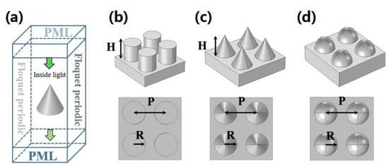
Figure 22.
GaN nanorods with different morphologies [264]: (a) schematic representation of a three-dimensional simulation model of a GaN nanoarray; (b) cylinder; (c) cone; and (d) hemisphere.
5.3. Solar Cells Based on Pyramidal Low-Dimensional Semiconductors
Solar cells directly convert light energy into electrical energy through photoelectric or photochemical processes [266]. The basic principle of a solar cell involves the formation of a new electron-hole pair upon the absorption of solar energy by a semiconductor P-N junction. Under the action of the built-in electric field of the P-N junction, the photogenerated holes flowed to the N region, and a current was generated within the circuit (Figure 23). In current research, both PSQDs and PSNRs have been used, and theoretical studies have confirmed that the photoelectric conversion efficiencies of QD superlattice solar cells should exceed 70% [267]. Thus, to obtain efficient QD solar cells, one of three possible conditions must be met. Firstly, the diffusion length of the minority carrier in the solid QD array must exceed the absorption length of the band edge by >1 μm. Alternatively, significant densification of the QD solid can be employed to reduce the absorption length of the photons near the band edge. Moreover, advanced photonic strategies can be used to increase light absorption in the active media with only single-pass absorbance.
Figure 23.
Basic principle of solar cells [266]: (a) schematic representation of a working solar cell; and (b) orbital hybridization of the donor (D) and acceptor (A) units in a D–A conjugated polymer of an organic solar cell.
In the context of III–V PSQD solar cells, Rashidinejad et al. studied the effect of the electro-elastic field on quantum nanostructured solar cells and discovered that the coupling between nanostructures in pyramidal InAs/GaAs QDs has a great impact on the induced strain, and maximum alternation of ~37% is present close to the boundary [268]. They also found that the induced strain and piezoelectric barrier are highly dependent on the geometry of an InAs QD, wherein the initial mismatch strain of a pyramidal InAs QD system significantly increases the induced strain by up to 52%. In contrast, Jaouane et al. studied the influence of the QD density on the photovoltaic conversion efficiencies of InAs/GaAs QD intermediate band solar cells and reported that the efficiency strongly depended on the confinement effect, the number of QDs, the QD density, and the coupling strength [269]. More specifically, in the case of InAs/GaAs QDs exhibiting the smallest barrier width, tallest QDs, and highest QD density, the photovoltaic conversion efficiency increased to 17.8807%. In addition, Sun et al. used a numerical simulation method to study the photoelectric properties of GaAs nanostructures with different shapes and observed that an increase in the bottom diameter of the nano-cone structure can significantly enhance the optical absorption performance of the GaAs nanoarray [270]. In fact, compared with the nano-cone structure, the truncated nano-cone structure exhibits a superior photoelectric conversion ability, which can facilitate the development of novel high-performance solar cells. In another study, Dash et al. exploited the finite element method to examine the influence of the wetting layer on the electronic intrinsic state of InP/InGaP QD solar cells [271]. They found that the ground state energy of the QDs can be calculated using the time-independent Schrodinger equation with the effective mass approximation, and this energy is affected by the size of the QD and the wetting layer of the quantum well that is associated with the QD. Indeed, the ground state is a confined intrinsic energy state without any nodes in the z-direction, which represents the real QD state. In contrast, the nodes of the higher excited state are in the r- or z-direction, which does not represent the real QD state.
To develop III-nitride PSQD solar cells, Arefinia et al. studied the intrinsic loss of InAs(1−x)Nx QD intermediate-band solar cells [272]. They found that when the concentration of N was <1%, the minimum total loss of the InAs(1−x)Nx QD intermediate-band solar cells was ~27%. Since the encapsulation of an inorganic shell on the QD core can eliminate the discontinuity of the core/ligand interface, partially eradicate surface defects, and protect the interaction between the core and surrounding environment, these core-shell QDs tend to possess improved physicochemical properties and stabilities [273]. Consequently, in recent years, researchers have focused on the photoelectric properties of pyramidal core-shell QDs. In this context, Jing et al. prepared a pyramidal InP/ZnSe QD light-emitting solar concentrator with a core-shell structure via the hot-injection method and studied its exciton dynamics [274]. It was discovered that a thicker ZnSe shell could stabilize the 1Pe energy state of the InP core and reduce the spectral overlap over the entire QD, which is conducive to the preparation of an efficient light-emitting solar concentrator (Figure 24). Moreover, under simulated sunlight irradiation, the optical efficiency reached 2.5%, and the power conversion efficiency reached 2.0% (5 × 5 × 0.5 cm3).
Figure 24.
Exciton dynamics in a pyramidal InP/ZnSe quantum dot solar concentrator [274]: (a) energy level diagram of the InP/ZnSe quantum dots consisting of three layers; (b) energy level diagram of the InP/ZnSe quantum dots consisting of nine layers; and (c) schematic representation of the method used to prepare InP/ZnSe quantum dots.
In addition to PSQDs, researchers have studied the properties of PSNR solar cells. For example, Chandrakala et al. employed a hydrothermal method to synthesize one-dimensional pyramidal rutile TiO2 NRs, wherein the absorption band edge of the pyramidal NRs was 377 nm and the band gap was 4.7 eV [275]. Importantly, they observed that the total solar cell efficiency of three-dimensional TiO2 nanoflowers composed of pyramidal NRs was approximately five times higher than that of the pure NRs. This difference was attributed to the enhanced light response performance of the TiO2 nanoflowers compared to that of pyramidal NRs, which in turn is due to the superior light scattering ability of the TiO2 nanoflowers, which imparts them with an excellent light capture ability. In another study, Huang et al. employed plasma in the preparation of high-quality pyramidal ZnO NR arrays as anti-reflection layers for c-Si solar cells [276]. They reported that the resulting solar cell achieved a photovoltaic conversion efficiency of 20.23%, which is conducive to improving the photoelectric performances of solar cells in practical applications. Furthermore, Wang et al. studied the performances of perovskite solar cells based on pyramidal TiO2 NRs co-doped with rare earth ions (i.e., Er3+ and Yb3+) [277]. As a result, the current density of the upconversion Er3+ and Yb3+ co-doped devices increased by 25%, the photon-electron conversion efficiency increased by 17%, and the optimal efficiency of the solar cell reached 10.02%. In addition, the Er3+ and Yb3+ co-doped devices exhibited near-infrared effects and achieved a conversion efficiency of 0.1% under infrared light irradiation (800–1100 nm). This property is beneficial for broadening the photoelectric responses of solar cells in the near-infrared region to ultimately improve the rate of sunlight utilization. It is worth mentioning that the presence of rare-earth ions inhibits the growth rate of the TiO2 NRs along certain crystal planes, such that the tip of the TiO2 NR appears pyramidal in shape. This feature is similar to the growth mechanism of the doped pyramidal ZnO NRs described in Section 2.2.1 [143,144]. In their investigation into the performances of InP NWR solar cells with different pyramidal shapes, Agnihotri et al. found that the optical short-circuit current density (Jsc) of a hybrid hexagonal pyramidal NWR solar cell was 34.2 mA/cm2, which is higher than that of the corresponding hexagonal NWRs (32.5 mA/cm2) and hexagonal nano-cones (32.86 mA/cm2) (Figure 25) [278]. Moreover, the energy conversion efficiency of the hybrid hexagonal pyramidal NWR solar cell was also superior to those of the hexagonal NWRs and the hexagonal nano-cones, with values of 19.15% (P-N junction) and 23% (P-I-N junction) being reached, respectively. This can be attributed to the fact that the optimized InP hybrid hexagonal pyramidal NWR solar cell exhibits a superior level of light capture in the absorption layer. In another study, Mishra et al. used carbon QDs and N-doped carbon QDs to modify pyramidal Si NWR arrays [279]. They found that the N-doped carbon QD-modified pyramidal Si NWR heterostructure exhibited significantly improved light absorption properties (i.e., 1.6 times stronger) than Si NWRs that were coated with carbon QDs on their surfaces. This effect is caused by the N-doped carbon QDs acting as a good absorption layer, thereby enhancing the light absorption ability of the pyramidal Si NWR array.
Figure 25.
Structures and photoelectric performances of different InP nanowires [278]: (a) a hexagonal nanowire; (b) the absorption spectra for hexagonal nanowires of different diameters (D) at a fixed filling ratio (FR) of 0.5. The corresponding optical Jsc plot is shown in the inset; (c) absorption spectra for hexagonal nanowires at an optimized D of 180 nm and with different FRs (0.3–0.9). The corresponding optical Jsc plot is shown in the inset; (d) A hexagonal nanopyramid; (e) the absorption spectra for hexagonal nanopyramids of different diameters (D) at a fixed FR of 0.7. The corresponding optical Jsc plot is shown in the inset; (f) absorption spectra for hexagonal nanopyramids at an optimized D of 260 nm and with different FRs (0.5–1.0). The corresponding optical Jsc plot is shown in the inset; (g) a hybrid hexagonal pyramidal nanowire; (h) the absorption spectra for hybrid hexagonal pyramidal nanowires of different diameters (D) at a fixed FR of 0.6. The corresponding optical Jsc plot is shown in the inset; and (i) generation rate profiles of InP hybrid hexagonal pyramidal nanowire solar cells with different diameters over two wavelength ranges (i.e., λ = 300–700 nm and λ = 700–950 nm).
5.4. Luminescent Devices Based on Pyramidal Low-Dimensional Semiconductors
When electrons are transferred from the high-energy state to the low-energy state in the conduction band, the systemic energy decreases. If systemic energy is released in the form of photons, it is known as a radiation transition. This corresponds to the luminescence process of the semiconductor and is essentially the recombination of electron-hole pairs. Electrons can be excited to a high-energy state via electrical and light excitation; therefore, the characteristics of semiconductor luminescence can be divided into electroluminescence (EL) and PL, among which EL is mainly associated with light-emitting diodes (LEDs) and lasers [280,281,282]. More specifically, an LED is a semiconductor device that can emit visible or invisible radiation when a forward current is applied to a P-N junction. QD-based LEDs have the advantages of possessing a narrow emission bandwidth and a band gap that can be tuned by changing the size, chemical composition, and internal structure (Figure 26) [283,284].
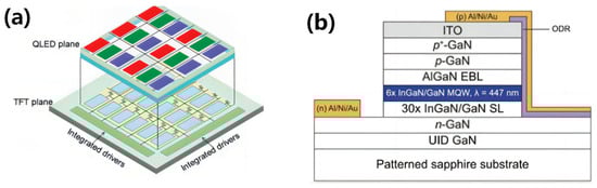
Figure 26.
Typical light-emitting diode (LED) structures: (a) schematic illustration of the proposed structure of an AM-QLED display [283]; and (b) schematic representation of the cross-sectional structure of an LED device [284].
Compared with organic molecules, semiconductor QDs have no inherent limitation on the maximum EL efficiency imposed by the spin selection law, and they ordinarily display only a small dark–bright exciton splitting (1–15 meV), thereby ensuring that efficient thermally excited dark excitons enter the bright state at room temperature [285,286,287]. Accordingly, semiconductor QDs are not affected by the statistical limitations of organic LEDs. Baier et al. initially prepared pyramidal multilayer heterostructure QDs on a GaAs(111)B substrate [288]. By studying the EL performance of a QD-based LED, it was found that the EL of a single pyramidal QD could be realized in a P-I-N junction with an injection current as low as 150 nA. Moreover, selective carrier injection into 20 nm-wide self-growing vertical quantum wires in the QD was able to suppress the emission of the parasitic lateral barrier, thereby significantly improving the device efficiency. Chung et al. also prepared pyramidal QDs on a GaAs(111)B substrate and reported that a micron-sized P-I-N junction composed of these QDs could be utilized as a spatially ordered and scalable electrically driven polarization-entangled photon source array with high entanglement quality [289]. Moreover, Chua et al. prepared a phosphorus-free pyramidal InGaN/GaN QD white-light LED and discovered that the internal quantum efficiency of the QD reached up to 50% at room temperature [290]. In another study, Rokhi et al. evaluated a ridge waveguide super-radiance LED based on truncated pyramidal GaN QDs and observed that QDs with an uneven size distribution produced larger spectral widths, thereby leading to higher output powers [291]. They also found that the output power of the ridge waveguide super-radiance LED decreased with an increase in temperature (Figure 27).
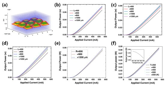
Figure 27.
Electroluminescence characteristics of truncated pyramidal GaN quantum dots [291]: (a) schematic representation of the ensemble of truncated pyramidal quantum dots in a cubical matrix; (b–d) plots of the output power as a function of the applied current for different cavity lengths (L), the curvature radii (R), and the power losses (αb), (a) R = 1200 μm, αb = 0.0596 m−1, (b) R = 900 μm, αb = 210.3342 m−1, and (c) R = 600 μm, αb = 3200.12 m−1; (e) plot of the output power as a function of the applied current for different curvature radii, where the length of the cavity was considered equal to 600 μm; (f) plot of the output power as a function of the bias current over five different temperatures for the GaN/AlGaN quantum dot super-luminescent light-emitting diode. Inset: output power versus temperature at a fixed current of 550 mA.
Lasers are another luminescent device that excite the electrons of atoms and molecules to higher energy levels. In recent years, the development of lasers has evolved into the field of nanosecond lasers, which are often based on QD systems [292]. QD lasers are particularly advantageous due to their low threshold currents, high characteristic temperatures, large differential gains, and large modulation bandwidths compared to conventional quantum well lasers [293]. Figure 28 shows two typical laser structures.
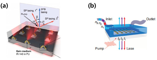
Figure 28.
Typical laser structures [292]: (a) schematic representation of a lattice plasmon laser based on the gold bowtie array; and (b) scheme representation of a real-time tunable plasmon crystal laser.
In terms of the laser properties of III–V PSQDs, InAs/GaAs and InGaAs/GaAs QDs have received particular attention [294]. For example, Asryan et al. found that the general relationship between the gain and the spontaneous emission spectrum holds for any number of radiation transitions and any distribution of QD sizes in the equilibrium-state filling of QDs [295]. In addition, depending on the separation between the transition energies, any inhomogeneous broadening, and the maximum gain value of the transition, the lasing wavelength can change either smoothly or in a stepwise manner upon variation in the loss. Because of the small overlap integral of a pyramidal InAs QD transition along with the large spontaneous emission lifetime, the single-layer mode gain is low, thereby rendering it impossible for the shallow cavity to achieve lasing through the ground state transition. With these considerations in mind, Qasaimeh et al. studied the influence of non-uniform spectral line broadening on the gain and differential gain properties of InAs/GaAs QD lasers [296]. They found that when the size fluctuation increased, the gain peak appeared to be red-shifted. More specifically, with a 130 Å average base length for the pyramidal QD and a standard deviation of 7 Å, the energy detuning between the gain peak and the differential gain peak is ~12 meV. Thus, nonuniform spectral broadening leads to early gain saturation and has a strong effect on the differential gain and optimal operating point of the laser. In another study, Vukmirovic et al. investigated the application of InAs/GaAs QDs in the field of mid-infrared pump lasers [297]. Using the eight-band k·p model and taking into account the interactions between the electron–longitudinal optical and acoustic phonons, they found that compared with quantum well-based pump lasers, the long carrier lifetimes of the QDs led to a lower pump flux, wherein both surface emission and edge emission were possible, and the spectral range of the laser emission reached 13–21 μm. Furthermore, Bhattacharya et al. investigated the laser properties of pyramidal InGaAs/GaAs QDs and found that the typical threshold current of the 200 μm long wavelength room temperature laser ranged from 6 to 20 mA, while the small signal modulation bandwidth range of the ridge waveguide laser increased from 5–7.5 GHz at 300 K to >20 GHz at 80 K [298]. Nevertheless, owing to the effect of electron-hole scattering, the modulation bandwidth is limited to ~6 GHz (300 K) and >20 GHz (80 K), severally. Furthermore, Borji et al. evaluated the band tunability of truncated pyramidal InxGa1−xAs/GaAs QD lasers and reported that an increase in the In content led to a reduced band gap and lower recombination energy for the electron-hole pairs; notably, this decreasing trend was nonlinear (Figure 29) [299].
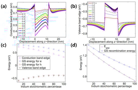
Figure 29.
Band tunability of truncated pyramidal InxGa1−xAs/GaAs quantum dot lasers [299]: (a,b) variation in the conduction and valence band edges at different indium ratios; and (c,d) variation in the energy gap and recombination energy (photon energy) of the ground state (GS) as a function of the indium ratio together.
5.5. Quantum Information Applications Based on Pyramidal Low-Dimensional Semiconductors
The quantum information theory is based on a novel method that employs the alteration of different states of a quantum system to realize information transmission [300]. More specifically, by taking advantage of the various coherence characteristics of quantum systems (i.e., quantum parallelism, quantum entanglement, and quantum no-cloning properties), new information methods for computing, coding, and information transmission have been developed [301,302,303]. Indeed, quantum information primarily involves the use of quantum computing. Moreover, the manipulation of single-photon quantum states using the unique physical properties of low-dimensional nanomaterials is currently a popular research topic. In the context of single-photon emission, Baier et al. were the first to discover this phenomenon in pyramidal InGaAs QDs [304]. Subsequently, other research groups reported the observation of single exciton peaks in InAs and GaN QDs [305,306]. In addition, Perez et al. studied the near-red light emission of pyramidal InGaN QDs and found that the PL emission energy of the QDs was ~2.03 eV, while the decay time was 1.4 ns [307]. They also noted that the stable behavior of the radiation attenuation confirmed the zero-dimensional characteristics of this system. The single-photon emission of truncated pyramidal GaN/AlN QDs has also been demonstrated at temperatures up to 350 K [308]. In recent years, the work of Kim et al. on the single-photon emission of QDs has attracted the most attention [309]. They discovered that the site-controlled InGaN formed at the apex of the Ag-coated GaN nano-cone structure can produce bright and unidirectionally emitting QDs, whereas the majority of light extracted from the QDs is directed toward the bottom of the pyramid (Figure 30a). Subsequently, Zhang et al. fabricated a structurally optimized single-quantum emitter that exhibited an enhanced extraction efficiency of 97.2% (from an initial value of 91.3%) at a wavelength of 520 nm [310]. This emitter exhibited ultra-brightness, good optical stability, and directional emission characteristics (Figure 30b). Moreover, with the introduction of a ZnO layer on the original quantum emitter to directly modify the surface structure into rough conical patterns, the extraction efficiency was improved compared with the original device.
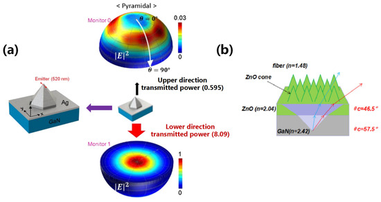
Figure 30.
Pyramidal quantum dot single photon emitters: (a) the maximum intensity value of the upper hemisphere (0.03) is normalized by that of the lower hemisphere [309]; and (b) schematic illustration of light ray incident at various angles from a quantum dot with a GaN/ZnO/ZnO conical surface [310].
The quantum entanglement effect based on PSQDs is expected to have important applications in the field of quantum information. In a theoretical study of entangled photons, Gershoni analyzed the entangled photon states of pyramidal QDs (Figure 31a), and discovered that the splitting of the exciton energy levels of pyramidal QDs is equivalent to the radiation width [311]; this is an important prerequisite for realizing an observable entanglement between the polarization state of the biexciton photons and that of the exciton photons. Moreover, they reported that when the exciton radiation width is significantly larger than its energy-level splitting, the interaction between light and matter is enhanced, thereby improving the performance of the semiconductor QDs. In another study, Juska et al. discovered that polarized entangled photons in pyramidal QDs violate Bell’s inequality, thereby indicating their strong potential for applications in integrated quantum information processing devices [312]. Furthermore, Huang et al. studied the controllable exciton-cavity mode interactions mediated by pure dephasing in a single spatially ordered quantum dot-nanocavity system, and found that upon varying the degree of detuning, Purcell-enhanced dynamics and phonon-assisted cavity feeding dominate the exciton-cavity mode interactions [313]. Additionally, during their investigation of PSQD material systems, Juska et al. found that high-density pyramidal InGaAs1−xNx QDs can emit polarized entangled photons without external manipulation of the quantum states (Figure 31b) [314]. Indeed, a region containing at least 15% entangled photon emitters was easily discovered. Subsequently, the same research group has studied the polarization entanglement conditions required to achieve photon emission from pyramidal In0.25Ga0.75As QDs (Figure 31c) [315]. It was deduced that a number of limitations affect the performances of high-density entangled photon emitters, such as the splitting of a small fine structure. In addition, effective QD charging under non-resonant excitation conditions was found to greatly reduce the number of useful biexciton–exciton recombination events. Consequently, Juska et al. solved the charging problem associated with QDs using dual-wavelength excitation technology, which will be essential in the further design and optimization of the spatially ordered QD structure for optical quantum information processing.
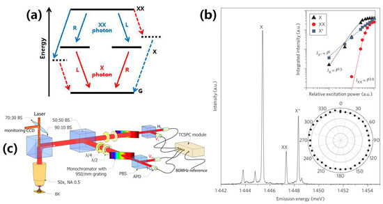
Figure 31.
The quantum entanglement effect of pyramidal semiconductor quantum dots: (a) a biexciton (XX) decays through the intermediate exciton (X) state to the ground (G) state by means of emitting two photons with opposite circular polarizations (L, left; R, right). If the exciton level is non-degenerate (dashed levels), then the two photons (dashed arrows) are collinearly polarized and the paths can be distinguished by their energies (indicated by different colors). Consequently, they are not entangled. In a symmetric quantum dot, the exciton level is degenerate (solid levels). The two photons (solid arrows) are cross-circularly polarized and so their decay path is not revealed by their energies. Consequently, they are entangled [311]; (b) Typical photoluminescence spectrum of a quantum dot. The exciton, biexciton, and generic charged exciton transitions are identified as X, XX, and X*, respectively [314]; and (c) micro-photoluminescence setup arranged for the polarization entanglement measurements [315].
6. Summary and Perspectives
Pyramidal low-dimensional semiconductors are widely used in various fields of optoelectronics, including photocatalysis, photodetection, solar cells, light-emitting diodes (LEDs), lasers, and quantum information devices. To date, the photoelectric properties of type III–V pyramidal semiconductor quantum dots (PSQDs) and type III-nitride PSQDs have received the greatest amount of research attention. Although type II–VI PSQDs have received less attention, their excellent photoelectric performances are beginning to emerge. It has been deduced that the photoelectric properties of PSQDs are closely related to their structures and shapes, wherein variations in the base width/height ratio have been demonstrated to exhibit an enormous influence on the separation of electron-hole pairs (excitons). However, the large-scale preparation of high-quality PSQDs remains an ongoing issue that must be addressed to achieve the diversification of PSQD structures to further improve their room temperature photoelectric performances (including the photoelectric responsivity, quantum efficiency, photoelectric conversion rate, photocatalytic efficiency, photon extraction rate, and gain coefficient of PSQDs). In the context of pyramidal semiconductor nanorods (PSNRs), nanomaterials based on ZnO, CoO, GaN, TiO2, InP, and Si components have received significant attention. Compared to PSQDs, PSNRs and pyramidal semiconductor nanowires (PSNWRs) exhibit larger specific surface areas, greater absorbance properties, and higher quantum efficiencies; therefore, the application of such materials as light receptors (e.g., photocatalysts, photodetectors, and solar cells) is currently a hot research topic. However, the preparation of PSNRs and PSNWRs often requires exceptional conditions, such as a specific pH, a carefully tuned doped-ion concentration, and an applied electric field. Similar to the problems encountered with PSQDs, the large-scale preparation of PSNRs remains a key bottleneck in achieving the practical application of these materials.
In the future, the leading research direction for pyramidal low-dimensional semiconductors will be related to the integration of optoelectronic devices, among which nanomaterials are expected to contribute to the most important progress in the fields of quantum information and solar cells. With the rapid development of information technology, humans require computers with greater computing power. PSQDs are among the main candidates for quantum-information materials owing to their superior optical quantum properties. Therefore, optimizing the structure of QDs, improving the manipulation of optical quantum states, and achieving truly effective applications are key challenges that researchers must solve. Because the research and development of solar cells are related to energy transformations, the superior photoelectric conversion performances exhibited by pyramidal low-dimensional nanomaterials are a key driving force that has attracted researchers to delve deeper into this field. Consequently, improving the photoelectric conversion efficiencies, realizing large-scale preparations, and prolonging the lifetimes of solar cells must be achieved. It is known that photodetectors based on pyramidal low-dimensional semiconductors possess higher intra-band absorption properties and stronger photon capture rates, which can allow the light response frequency to be adjusted. Therefore, array detectors composed of this material have become a novel evolution trend. For pyramidal photocatalytic nanomaterials, it is necessary to focus on the construction of composite structures and the optimization of preparation technologies to obtain low-cost nanomaterials with high catalytic efficiencies. In the context of light-emitting diodes, PSQDs are advantageous due to their lower injection currents, and the integration of multiple PSQDs can improve the output power and save energy. However, compared with spherical and plate QDs, the development of PSQDs is slow in lasers. Therefore, it is a great challenge to realize the faster radiative and slower Auger recombination times of PSQDs. In this review, new requirements related to the design, size, and performance of devices based on pyramidal low-dimensional semiconductors were proposed in terms of the materials and structures to promote their synergistic development.
Author Contributions
Conceptualization, H.L. and A.J.; writing—original draft preparation, A.J., S.X., Q.C. and M.L.; writing—review and editing, H.L., A.J. and S.X.; project administration, H.L.; funding acquisition, H.L. All authors have read and agreed to the published version of the manuscript.
Funding
This research was funded by Henan Province Science and Technology Research Project (222102230084), Open Fund of Henan International Joint Laboratory of Nano-photoelectric Magnetic Materials, Cultivation Programme for Young Backbone Teachers in Henan University of Technology, Science and Technology Key Project from Education Department of Henan Province (21A430011).
Institutional Review Board Statement
Not applicable.
Informed Consent Statement
Not applicable.
Data Availability Statement
Not applicable.
Acknowledgments
The authors would like to thank financial support from the Henan Province Science and Technology Research Project (222102230084), Open Fund of Henan International Joint Laboratory of Nano-photoelectric Magnetic Materials, Cultivation Programme for Young Backbone Teachers in Henan University of Technology, Science and Technology Key Project from Education Department of Henan Province (21A430011).
Conflicts of Interest
The authors declare no conflicts of interest.
References
- Yetisen, A.K.; Qu, H.; Manbachi, A.; Butt, H.; Dokmeci, M.R.; Hinestroza, J.P.; Skorobogatiy, M.; Khademhosseini, A.; Yun, S.H. Nanotechnology in textiles. ACS Nano 2016, 10, 3042–3068. [Google Scholar] [CrossRef] [PubMed]
- Malik, S.; Muhammad, K.; Waheed, Y. Nanotechnology: A revolution in modern industry. Molecules 2023, 28, 661. [Google Scholar] [CrossRef] [PubMed]
- Hussein, A.K. Applications of nanotechnology in renewable energies—A comprehensive overview and understanding. Renew. Sustain. Energy Rev. 2015, 42, 460–476. [Google Scholar] [CrossRef]
- Guerra, F.D.; Attia, M.F.; Whitehead, D.C.; Alexis, F. Nanotechnology for environmental remediation: Materials and applications. Molecules 2018, 23, 1760. [Google Scholar] [CrossRef] [PubMed]
- Ramesh, M.; Janani, R.; Deepa, C.; Rajeshkumar, L. Nanotechnology-enabled biosensors: A review of fundamentals, design principles, materials, and applications. Biosensors 2022, 13, 40. [Google Scholar] [CrossRef]
- Blancon, J.C.; Even, J.; Stoumpos, C.C.; Kanatzidis, M.G.; Mohite, A.D. Semiconductor physics of organic–inorganic 2D halide perovskites. Nat. Nanotechnol. 2020, 15, 969–985. [Google Scholar] [CrossRef] [PubMed]
- Hirohata, A.; Takanashi, K. Future perspectives for spintronic devices. J. Phys. D Appl. Phys. 2014, 47, 193001. [Google Scholar] [CrossRef]
- Farahani, R.D.; Dubé, M.; Therriault, D. Three-dimensional printing of multifunctional nanocomposites: Manufacturing techniques and applications. Adv. Mater. 2016, 28, 5794–5821. [Google Scholar] [CrossRef] [PubMed]
- Abo-Hamad, A.; Hayyan, M.; AlSaadi, M.A.; Hashim, M.A. Potential applications of deep eutectic solvents in nanotechnology. Chem. Eng. J. 2015, 273, 551–567. [Google Scholar] [CrossRef]
- Makam, P.; Gazit, E. Minimalistic peptide supramolecular co-assembly: Expanding the conformational space for nanotechnology. Chem. Soc. Rev. 2018, 47, 3406–3420. [Google Scholar] [CrossRef] [PubMed]
- Amarnath, C.A.; Nanda, S.S.; Papaefthymiou, G.C.; Yi, D.K.; Paik, U. Nanohybridization of low-dimensional nanomaterials: Synthesis, classification, and application. Crit. Rev. Solid State Mater. Sci. 2013, 38, 1–56. [Google Scholar] [CrossRef]
- Cao, Y.; Fatemi, V.; Fang, S.; Watanabe, K.; Taniguchi, T.; Kaxiras, E.; Jarillo-Herrero, P. Unconventional superconductivity in magic-angle graphene superlattices. Nature 2018, 556, 43–50. [Google Scholar] [CrossRef] [PubMed]
- Chiang, W.S.; Fratini, E.; Baglioni, P.; Chen, J.H.; Liu, Y. Pore size effect on methane adsorption in mesoporous silica materials studied by small-angle neutron scattering. Langmuir 2016, 32, 8849–8857. [Google Scholar] [CrossRef] [PubMed]
- Niu, D.; Tang, G.H. The effect of surface wettability on water vapor condensation in nanoscale. Sci. Rep. 2016, 6, 19192. [Google Scholar] [CrossRef] [PubMed]
- Awschalom, D.D.; Smyth, J.F.; Grinstein, G.; Divincenzo, D.P.; Loss, D. Macroscopic quantum tunneling in magnetic proteins. Phys. Rev. Lett. 1992, 68, 3092–3095. [Google Scholar] [CrossRef] [PubMed]
- Wu, P.; Xu, Y.X.; Zhan, J.Y.; Li, Y.; Xue, H.G.; Pang, H. The research development of quantum dots in electrochemical energy storage. Small 2018, 14, 1801479. [Google Scholar] [CrossRef] [PubMed]
- Vajner, D.A.; Rickert, L.; Gao, T.; Kaymazlar, K.; Heindel, T. Quantum communication using semiconductor quantum dots. Adv. Quantum Technol. 2022, 5, 2100116. [Google Scholar] [CrossRef]
- Malhotra, A.; Maldovan, M. Phononic pathways towards rational design of nanowire heat conduction. Nanotechnology 2019, 30, 372002. [Google Scholar] [CrossRef] [PubMed]
- Wu, G.L.; Cheng, Y.H.; Yang, Z.H.; Jia, Z.R.; Wu, H.J.; Yang, L.J.; Li, H.L.; Guo, P.Z.; Lv, H.L. Design of carbon sphere/magnetic quantum dots with tunable phase compositions and boost dielectric loss behavior. Chem. Eng. J. 2018, 333, 519–528. [Google Scholar] [CrossRef]
- Yin, R.; Yang, S.Y.; Li, Q.M.; Zhang, S.D.; Liu, H.; Han, J.; Liu, C.T.; Shen, C.Y. Flexible conductive Ag nanowire/cellulose nanofibril hybrid nanopaper for strain and temperature sensing applications. Sci. Bull. 2020, 65, 899–908. [Google Scholar] [CrossRef] [PubMed]
- Mitzinger, S.; Broeckaert, L.; Massa, W.; Weigend, F.; Dehnen, S. Understanding of multimetallic cluster growth. Nat. Commun. 2016, 7, 10480. [Google Scholar] [CrossRef]
- Zhang, J.; Zhang, S.H.; Zhang, Y.L.; Al-Hartomy, O.; Wageh, S.; Al-Sehemi, A.G.; Hao, Y.B.; Gao, L.F.; Wang, H.; Zhang, H. Colloidal quantum dots: Synthesis, composition, structure, and emerging optoelectronic applications. Laser Photonics Rev. 2023, 17, 2200551. [Google Scholar] [CrossRef]
- Maenosono, S.; Okubo, T.; Yamaguchi, Y. Overview of nanoparticle array formation by wet coating. J. Nanopart. Res. 2003, 5, 5–15. [Google Scholar] [CrossRef]
- Rackauskas, S.; Nasibulin, A.G. Nanowire growth without catalysts: Applications and mechanisms at the atomic scale. ACS Appl. Nano Mater. 2020, 3, 7314–7324. [Google Scholar] [CrossRef]
- Drake, G.A.; Keating, L.P.; Shim, M. Design principles of colloidal nanorod heterostructures. Chem. Rev. 2022, 123, 3761–3789. [Google Scholar] [CrossRef]
- Tenne, R.; Rao, C.N.R. Inorganic nanotubes. Philos. Trans. R. Soc. Lond. Ser. A Math. Phys. Eng. Sci. 2004, 362, 2099–2125. [Google Scholar] [CrossRef] [PubMed]
- Li, D.M.; Cheng, Y.Y.; Luo, Y.X.; Teng, Y.Q.; Liu, Y.H.; Feng, L.B.; Wang, N.; Zhao, Y. Electrospun nanofiber materials for photothermal interfacial evaporation. Materials 2023, 16, 5676. [Google Scholar] [CrossRef]
- Wang, Z.L. ZnO nanowire and nanobelt platform for nanotechnology. Mater. Sci. Eng. R Rep. 2009, 64, 33–71. [Google Scholar] [CrossRef]
- Liu, Y.X.; Chen, E.Q. Polymer crystallization of ultrathin films on solid substrates. Coord. Chem. Rev. 2010, 254, 1011–1037. [Google Scholar] [CrossRef]
- Dai, Z.; Ansaloni, L.; Deng, L. Recent advances in multi-layer composite polymeric membranes for CO2 separation: A review. Green Energy Environ. 2016, 1, 102–128. [Google Scholar] [CrossRef]
- Ning, J.J.; Duan, Z.H.; Kershaw, S.V.; Rogach, A.L. Phase-controlled growth of CuInS2 shells to realize colloidal CuInSe2/CuInS2 core/shell nanostructures. ACS Nano 2020, 14, 11799–11808. [Google Scholar] [CrossRef] [PubMed]
- Ouattara, L.; Mikkelsen, A.; Lundgren, E.; Borgström, M.; Samuelson, L.; Seifert, W. Stacked InAs quantum dots in InP studied by cross-sectional scanning tunnelling microscopy. Nanotechnology 2004, 15, 1701–1707. [Google Scholar] [CrossRef]
- Adhikari, S.; Lem, O.L.C.; Kremer, F.; Vora, K.; Brink, F.; Lysevych, M.; Tan, H.H.; Jagadish, C. Nonpolar AlxGa1–xN/AlyGa1–yN multiple quantum wells on GaN nanowire for UV emission. Nano Res. 2022, 15, 7670–7680. [Google Scholar] [CrossRef]
- Tu, C.G.; Zhang, X.; Chou, K.P.; Tse, W.F.; Hsu, Y.C.; Chen, Y.P.; Kiang, Y.W.; Yang, C.C. AlGaN nano–shell structure on a GaN nanorod formed with the pulsed MOCVD growth. Nanotechnology 2019, 30, 275201. [Google Scholar] [CrossRef] [PubMed]
- Chen, X.Q.; Liu, Y.H.; Wang, B.B.; Liu, X.T.; Lu, C. Understanding role of microstructures of nanomaterials in electrochemiluminescence properties and their applications. TrAC Trends Anal. Chem. 2023, 162, 117030. [Google Scholar] [CrossRef]
- Mishra, N.; Vasavi Dutt, V.G.; Arciniegas, M.P. Recent progress on metal chalcogenide semiconductor tetrapod-shaped colloidal nanocrystals and their applications in optoelectronics. Chem. Mater. 2019, 31, 9216–9242. [Google Scholar] [CrossRef]
- Goyal, M.; Singh, M. Size and shape dependence of optical properties of nanostructures. Appl. Phys. A 2020, 126, 176. [Google Scholar] [CrossRef]
- Wang, C.H.; Zhang, X.T.; Zhang, Y.L.; Jia, Y.; Yuan, B.; Yang, J.K.; Sun, P.P.; Liu, Y.C. Morphologically-tunable TiO2 nanorod film with high energy facets: Green synthesis, growth mechanism and photocatalytic activity. Nanoscale 2012, 4, 5023–5030. [Google Scholar] [CrossRef] [PubMed]
- Rawat, K.; Goyal, M. Modelling to determine the variation of magnetic properties with size and shape in the nanomaterials. Pramana 2021, 95, 184. [Google Scholar] [CrossRef]
- Huang, M.H. Facet-dependent optical properties of semiconductor nanocrystals. Small 2019, 15, 1804726. [Google Scholar] [CrossRef] [PubMed]
- Regulacio, M.D.; Han, M.Y. Composition-tunable alloyed semiconductor nanocrystals. Acc. Chem. Res. 2010, 43, 621–630. [Google Scholar] [CrossRef] [PubMed]
- Burda, C.; Chen, X.B.; Narayanan, R.; El-Sayed, M.A. Chemistry and properties of nanocrystals of different shapes. Chem. Rev. 2005, 105, 1025–1102. [Google Scholar] [CrossRef] [PubMed]
- Esteves, A.C.; Trindade, T. Synthetic studies on II/VI semiconductor quantum dots. Curr. Opin. Solid State Mater. Sci. 2002, 6, 347–353. [Google Scholar] [CrossRef]
- Jang, Y.J.; Shapiro, A.; Isarov, M.; Rubin-Brusilovski, A.; Safran, A.; Budniak, A.K.; Horani, F.; Dehnel, J.; Sashchiuk, A.; Lifshitz, E. Interface control of electronic and optical properties in IV–VI and II–VI core/shell colloidal quantum dots: A review. Chem. Commun. 2017, 53, 1002–1024. [Google Scholar] [CrossRef] [PubMed]
- Fan, G.; Wang, C.; Fang, J. Solution-based synthesis of III–V quantum dots and their applications in gas sensing and bio-imaging. Nano Today 2014, 9, 69–84. [Google Scholar] [CrossRef]
- Wong, P.S.; Liang, B.; Huffaker, D.L. InAs quantum dots on nanopatterned GaAs (001) surface: The growth, optical properties, and device implementation. J. Nanosci. Nanotechnol. 2010, 10, 1537–1550. [Google Scholar] [CrossRef] [PubMed]
- Lopez, M.; Ishikawa, T.; Nomura, Y. Molecular-beam epitaxial growth of pyramidal structures on patterned GaAs [100] substrates for three-dimensionally confined structures. Electron. Lett. 1993, 25, 2225–2227. [Google Scholar] [CrossRef]
- Taher, M.; Al-yousif, S.; Ahmed, N.M. Atomistic modeling of InGaN/GaN quantum dots-in-nanowire for graded surface-emitting low-threshold, blue exciton laser. Results Phys. 2021, 20, 103732. [Google Scholar] [CrossRef]
- Ranjbar Jahromi, I.; Juska, G.; Varo, S.; Basset, F.B.; Salusti, F.; Trotta, R.; Gocalinska, A.; Mattana, F.; Pelucchi, E. Optical properties and symmetry optimization of spectrally (excitonically) uniform site-controlled GaAs pyramidal quantum dots. Appl. Phys. Lett. 2021, 118, 073103. [Google Scholar] [CrossRef]
- Holsgrove, K.M.; O’Reilly, T.I.; Varo, S.; Gocalinska, A.; Juska, G.; Kepaptsoglou, D.M.; Pelucchi, E.; Arredondo, M. Towards 3D characterisation of site-controlled InGaAs pyramidal QDs at the nanoscale. J. Mater. Sci. 2022, 57, 16383–16396. [Google Scholar] [CrossRef] [PubMed]
- Liu, Y.; Bose, S.; Fan, W. Effect of size and shape on electronic and optical properties of CdSe quantum dots. Optik 2018, 155, 242–250. [Google Scholar] [CrossRef]
- Liang, L.; Xie, W. Influence of the shape of quantum dots on their optical absorptions. Phys. B Condens. Matter 2015, 462, 15–17. [Google Scholar] [CrossRef]
- Califano, M. Tetrahedral vs spherical nanocrystals: Does the shape really matter? Chem. Mater. 2024, 36, 1162–1171. [Google Scholar] [CrossRef]
- Diroll, B.T.; Guzelturk, B.; Po, H.; Dabard, C.; Fu, N.Y.; Makke, L.; Lhuillier, E.; Ithurria, S. 2D II–VI semiconductor nanoplatelets: From material synthesis to optoelectronic integration. Chem. Rev. 2023, 123, 3543–3624. [Google Scholar] [CrossRef]
- Mantashian, G.A. The contribution of edge number on the optical properties in ZnO pyramidal quantum dots. In Proceedings of the Conference on Quantum Optics and Photon Counting, Prague, Czech Republic, 26–27 April 2023. [Google Scholar]
- Oberli, D.Y.; Byszewski, M.; Chalupar, B.; Pelucchi, E.; Rudra, A.; Kapon, E. Coulomb correlations of charged excitons in semiconductor quantum dots. Phys. Rev. B 2009, 80, 165312. [Google Scholar] [CrossRef]
- Oberli, D.Y. Intertwining of Zeeman and Coulomb interactions on excitons in highly symmetric semiconductor quantum dots. Phys. Rev. B 2012, 85, 155305. [Google Scholar] [CrossRef]
- Surrente, A.; Felici, M.; Gallo, P.; Rudra, A.; Dwir, B.; Kapon, E. Dense arrays of site-controlled quantum dots with tailored emission wavelength: Growth mechanisms and optical properties. Appl. Phys. Lett. 2017, 111, 221102. [Google Scholar] [CrossRef]
- Zekavat, M.A.; Sabaeian, M.; Solookinejad, G. Graphene plasmonic coupling with intersubband radiation of truncated pyramidal-shaped InAs/GaAs quantum dots. JOSA B 2021, 38, 1824–1833. [Google Scholar] [CrossRef]
- Baira, M.; Salem, B.; Madhar, N.A.; Ilahi, B. Intersubband optical nonlinearity of GeSn quantum dots under vertical electric field. Micromachines 2019, 10, 243. [Google Scholar] [CrossRef] [PubMed]
- Lox, J.F.L.; Dang, Z.Y.; Dzhagan, V.M.; Spittel, D.; Martin-Garcia, B.; Moreels, I.; Zahn, D.R.T.; Lesnyak, V. Near-infrared Cu–In–Se-based colloidal nanocrystals via cation exchange. Chem. Mater. 2018, 30, 2607–2617. [Google Scholar] [CrossRef]
- Cho, B.; Baek, S.; Woo, H.G.; Sohn, H. Synthesis of silicon quantum dots showing high quantum efficiency. J. Nanosci. Nanotechnol. 2014, 14, 5868–5872. [Google Scholar] [CrossRef] [PubMed]
- Wei, F.D.; Lu, X.L.; Wu, Y.Z.; Cai, Z.; Liu, L.P.; Zhou, P.; Hu, Q. Synthesis of highly luminescent CdTe/CdS/ZnS quantum dots by a one-pot capping method. Chem. Eng. J. 2013, 226, 416–422. [Google Scholar] [CrossRef]
- Huang, F.; Huang, B. Aqueous synthesis of water-soluble citrate-modified cadmium selenide/cadmium sulfide/zinc sulfide quantum dots. Spectrosc. Lett. 2015, 48, 422–426. [Google Scholar] [CrossRef]
- Murphy, J.E.; Beard, M.C.; Norman, A.G.; Ahrenkiel, S.P.; Johnson, J.C.; Yu, P.R.; Micic, O.I.; Ellingson, R.J.; Nozik, A.J. PbTe colloidal nanocrystals: Synthesis, characterization, and multiple exciton generation. J. Am. Chem. Soc. 2006, 128, 3241–3247. [Google Scholar] [CrossRef] [PubMed]
- Zhang, Y.; Dai, Q.Q.; Li, X.B.; Liang, J.Y.; Colvin, V.L.; Wang, Y.D.; Yu, W.W. PbSe/CdSe and PbSe/CdSe/ZnSe hierarchical nanocrystals and their photoluminescence. Langmuir 2011, 27, 9583–9587. [Google Scholar] [CrossRef] [PubMed]
- Laufersky, G.; Bradley, S.; Frécaut, E.; Lein, M.; Nann, T. Unraveling aminophosphine redox mechanisms for glovebox-free InP quantum dot syntheses. Nanoscale 2018, 10, 8752–8762. [Google Scholar] [CrossRef] [PubMed]
- Cao, Y.W.; Banin, U. Growth and properties of semiconductor core/shell nanocrystals with InAs cores. J. Am. Chem. Soc. 2000, 122, 9692–9702. [Google Scholar] [CrossRef]
- Shamsi, J.; Rastogi, P.; Caligiuri, V.; Abdelhady, A.L.; Spirito, D.; Manna, L.; Krahne, R. Bright-emitting perovskite films by large-scale synthesis and photoinduced solid-state transformation of CsPbBr3 nanoplatelets. ACS Nano 2017, 11, 10206–10213. [Google Scholar] [CrossRef]
- Takeda, M.; Yokoyama, M.; Umemoto, K.; Lyu, B.; Takahashi, Y.; Rodbuntum, S.; Enomoto, J.; Tozawa, K.; Nohara, T.; Tabata, K.; et al. Synthesis of highly luminescent CH3NH3PbBr3 perovskite nanocrystals via a forced thin film reactor. Jpn. J. Appl. Phys. 2020, 59, SIIG02. [Google Scholar] [CrossRef]
- Saidzhonov, B.M.; Zaytsev, V.B.; Berekchiian, M.V.; Vasiliev, R.B. Highly luminescent copper-doped ultrathin CdSe nanoplatelets for white-light generation. J. Lumin. 2020, 222, 117134. [Google Scholar] [CrossRef]
- Kelestemur, Y.; Guzelturk, B.; Erdem, O.; Olutas, M.; Gungor, K.; Demir, H.V. Platelet-in-box colloidal quantum wells: CdSe/CdS@CdS core/crown@shell heteronanoplatelets. Adv. Funct. Mater. 2016, 26, 3570–3579. [Google Scholar] [CrossRef]
- Tan, R.; Yuan, Y.C.; Nagaoka, Y.; Eggert, D.; Wang, X.D.; Thota, S.; Guo, P.; Yang, H.R.; Zhao, J.; Chen, O. Monodisperse hexagonal pyramidal and bipyramidal wurtzite CdSe-CdS core-shell nanocrystals. Chem. Mater. 2017, 29, 4097–4108. [Google Scholar] [CrossRef]
- Langevin, M.A.; Ritcey, A.M.; Allen, C.N. Air-stable near-infrared AgInSe2 nanocrystals. ACS Nano 2014, 8, 3476–3482. [Google Scholar] [CrossRef] [PubMed]
- Li, R.F.; Lee, J.; Yang, B.C.; Horspool, D.N.; Aindow, M.; Papadimitrakopoulos, F. Amine-assisted facetted etching of CdSe nanocrystals. J. Am. Chem. Soc. 2005, 127, 2524–2532. [Google Scholar] [CrossRef] [PubMed]
- Chetty, S.S.; Praneetha, S.; Murugan, A.V.; Govarthanan, K.; Verma, R.S. Microwave-assisted synthesis of quasi-pyramidal CuInS2–ZnS nanocrystals for enhanced near-Infrared targeted fluorescent imaging of subcutaneous melanoma. Adv. Biosyst. 2019, 3, 1800127. [Google Scholar] [CrossRef] [PubMed]
- Hollinger, R.; Gupta, D.; Zapf, M.; Röder, R.; Kartashov, D.; Ronning, C.; Spielmann, C. Single nanowire defined emission properties of ZnO nanowire arrays. J. Phys. D Appl. Phys. 2019, 52, 295101. [Google Scholar] [CrossRef]
- Atkinson, J.; Goldthorpe, I.A. Near-infrared properties of silver nanowire networks. Nanotechnology 2020, 31, 365201. [Google Scholar] [CrossRef] [PubMed]
- Abhilash, T.S.; Mathew, J.P.; Sengupta, S.; Gokhale, M.R.; Bhattacharya, A.; Deshmukh, M.M. Wide bandwidth nanowire electromechanics on insulating substrates at room temperature. Nano Lett. 2012, 12, 6432–6435. [Google Scholar] [CrossRef] [PubMed]
- Qi, J.W.; Li, Y.D.; Yang, M.; Wu, Q.; Chen, Z.Q.; Peng, J.Y.; Liu, Y.; Wang, W.D.; Yu, X.Y.; Sun, Q.; et al. Fabrication of nanowire network AAO and its application in SERS. Nanoscale Res. Lett. 2013, 8, 495. [Google Scholar]
- Morales, A.M.; Lieber, C.M. A laser ablation method for the synthesis of crystalline semiconductor nanowires. Science 1998, 279, 208–211. [Google Scholar] [CrossRef] [PubMed]
- Zhang, W.; Yang, S. In situ fabrication of inorganic nanowire arrays grown from and aligned on metal substrates. Acc. Chem. Res. 2009, 42, 1617–1627. [Google Scholar] [CrossRef] [PubMed]
- Xiong, S.; Zhang, X.; Qian, Y. CdS with various novel hierarchical nanostructures by nanobelts/nanowires self-assembly: Controllable preparation and their optical properties. Cryst. Growth Des. 2009, 9, 5259–5265. [Google Scholar] [CrossRef]
- Zhu, J.; Xu, Z.H.; Ha, S.H.; Li, D.K.; Zhang, K.X.; Zhang, H.; Feng, J.J. Gallium oxide for gas sensor applications: A comprehensive review. Materials 2022, 15, 7339. [Google Scholar] [CrossRef] [PubMed]
- Shah, K.A.; Tali, B.A. Synthesis of carbon nanotubes by catalytic chemical vapour deposition: A review on carbon sources, catalysts and substrates. Mater. Sci. Semicond. Process. 2016, 41, 67–82. [Google Scholar] [CrossRef]
- Ruach-Nir, I.; Zhang, Y.; Popovitz-Biro, R.; Rubinstein, I.; Hodes, G. Shape control in electrodeposited, epitaxial CdSe nanocrystals on (111) gold. J. Phys. Chem. B 2003, 107, 2174–2179. [Google Scholar] [CrossRef]
- Li, Y.; Qian, F.; Xiang, J.; Lieber, C.M. Nanowire electronic and optoelectronic devices. Mater. Today 2006, 9, 18–27. [Google Scholar] [CrossRef]
- Jia, C.C.; Lin, Z.Y.; Huang, Y.; Duan, X.F. Nanowire electronics: From nanoscale to macroscale. Chem. Rev. 2019, 119, 9074–9135. [Google Scholar] [CrossRef] [PubMed]
- Shinagawa, T.; Shibata, K.; Shimomura, O.; Chigane, M.; Nomura, R.; Izaki, M. Solution-processed high-haze ZnO pyramidal textures directly grown on a TCO substrate and the light-trapping effect in Cu2O solar cells. J. Mater. Chem. C 2014, 2, 2908–2917. [Google Scholar] [CrossRef]
- Riley, J.R.; Padalkar, S.; Li, Q.M.; Lu, P.; Koleske, D.D.; Wierer, J.J.; Wang, G.T.; Lauhon, L.J. Three-dimensional mapping of quantum wells in a GaN/InGaN core–shell nanowire light-emitting diode array. Nano Lett. 2013, 13, 4317–4325. [Google Scholar] [CrossRef] [PubMed]
- Chen, K.M.; Jesson, D.E.; Pennycook, S.J.; Thundat, T.; Warmack, R.J. Critical nuclei shapes in the stress-driven 2D-to-3D transition. Phys. Rev. B 1997, 56, R1700–R1703. [Google Scholar] [CrossRef]
- Vailionis, A.; Cho, B.; Glass, G.; Desjardins, P.; Cahill, D.G.; Greene, J.E. Pathway for the strain-driven two-dimensional to three-dimensional transition during growth of Ge on Si(001). Phys. Rev. Lett. 2000, 85, 3672–3675. [Google Scholar] [CrossRef] [PubMed]
- Mo, Y.W.; Savage, D.E.; Swartzentruber, B.S.; Lagally, M.G. Kinetic pathway in the Stranski–Krastanow growth of Ge on Si(001). Phys. Rev. Lett. 1990, 65, 1020–1023. [Google Scholar] [CrossRef] [PubMed]
- Sutter, E.; Sutter, P.; Bernard, J.E. Extended shape evolution of low-mismatch Si1−xGex alloy islands on Si(100). Appl. Phys. Lett. 2004, 84, 2262–2264. [Google Scholar] [CrossRef]
- Stoffel, M.; Rastelli, A.; Tersoff, J.; Merdzhanova, T.; Schmidt, O.G. Local equilibrium and global relaxation of strained SiGe/Si(001) layers. Phys. Rev. B 2006, 74, 155326. [Google Scholar] [CrossRef]
- Rastelli, A.; von Känel, H. Island formation and faceting in the SiGe/Si(001) system. Surf. Sci. 2003, 532, 769–773. [Google Scholar] [CrossRef]
- Medeiros-Ribeiro, G.; Bratkovski, A.M.; Kamins, T.I.; Ohlberg, D.A.A.; Williams, R.S. Shape transition of germanium nanocrystals on a silicon (001) surface from pyramids to domes. Science 1998, 279, 353–355. [Google Scholar] [CrossRef] [PubMed]
- Ohlsson, B.J.; Björk, M.T.; Persson, A.I.; Thelander, C.; Wallenberg, L.R.; Magnusson, M.H.; Deppert, K.; Samuelson, L. Growth and characterization of GaAs and InAs nano-whiskers and InAs/GaAs heterostructures. Phys. E Low-Dimens. Syst. Nanostruct. 2002, 13, 1126–1130. [Google Scholar] [CrossRef]
- Imran, A.; Jiang, J.L.; Eric, D.; Zahid, M.N.; Yousaf, M.; Shah, Z.H. Optical properties of InAs/GaAs quantum dot superlattice structures. Results Phys. 2018, 9, 297–302. [Google Scholar] [CrossRef]
- Xu, M.C.; Temko, Y.; Suzuki, T.; Jacobi, K. Shape transition of InAs quantum dots on GaAs(001). J. Appl. Phys. 2005, 98, 083525. [Google Scholar] [CrossRef]
- Kratzer, P.; Liu, Q.K.K.; Acosta-Diaz, P.; Manzano, C.; Costantini, G.; Songmuang, R.; Rastelli, A.; Schmidt, O.G.; Kern, K. Shape transition during epitaxial growth of InAs quantum dots on GaAs(001): Theory and Experiment. Phys. Rev. B 2006, 73, 205347. [Google Scholar] [CrossRef]
- Fukui, T.; Kumakura, K.; Nakakoshi, K.; Motohisa, J. Pyramidal quantum dot structures by self-limited selective area metalorganic vapor phase epitaxy. Solid-State Electron. 1996, 40, 799–802. [Google Scholar]
- Hartmann, A.; Loubies, L.; Reinhardt, F.; Kapon, E. Self-limiting growth of quantum dot heterostructures on nonplanar {111}B substrates. Appl. Phys. Lett. 1997, 71, 1314–1316. [Google Scholar] [CrossRef]
- Pelucchi, E.; Baier, M.; Ducommun, Y.; Watanabe, S.; Kapon, E. High-quality InxGa1–xAs/Al0.30Ga0.70As quantum dots grown in inverted pyramids. Phys. Status Solidi B 2003, 238, 233–236. [Google Scholar] [CrossRef]
- Dimastrodonato, V.; Mereni, L.O.; Young, R.J.; Pelucchi, E. Growth and structural characterization of pyramidal site-controlled quantum dots with high uniformity and spectral purity. Phys. Status Solidi B 2010, 247, 1862–1866. [Google Scholar] [CrossRef]
- Prohl, C.; Lenz, A.; Roy, D.; Schuppang, J.; Stracke, G.; Strittmatter, A.; Pohl, U.W.; Bimberg, D.; Eisele, H.; Dähne, M. Spatial structure of In0. 25Ga0. 75As/GaAs/GaP quantum dots on the atomic scale. Appl. Phys. Lett. 2013, 102, 123102. [Google Scholar] [CrossRef]
- Gajjela, R.S.R.; Hendriks, A.L.; Douglas, J.O.; Sala, E.M.; Steindl, P.; Klenovsky, P.; Bagot, P.A.J.; Moody, M.P.; Bimberg, D.; Koenraad, P.M. Structural and compositional analysis of (InGa)(AsSb)/GaAs/GaP Stranski–Krastanov quantum dots. Light Sci. Appl. 2021, 10, 125. [Google Scholar] [CrossRef] [PubMed]
- Hasan, S.; Merckling, C.; Pantouvaki, M.; Meersschaut, J.; Van Campenhout, J.; Vandervorst, W. Thermodynamic modelling of InAs/InP(001) growth towards quantum dots formation by metalorganic vapor phase epitaxy. J. Cryst. Growth 2019, 509, 133–140. [Google Scholar] [CrossRef]
- Weng, G.E.; Ling, A.K.; Lv, X.Q.; Zhang, J.Y.; Zhang, B.P. III-Nitride-based quantum dots and their optoelectronic applications. Nano-Micro Lett. 2011, 3, 200–207. [Google Scholar] [CrossRef]
- Ramvall, P.; Riblet, P.; Nomura, S.; Aoyagi, Y.; Tanaka, S. Optical properties of GaN quantum dots. J. Appl. Phys. 2000, 87, 3883–3890. [Google Scholar] [CrossRef]
- Korytov, M.; Benaissa, M.; Brault, J.; Huault, T.; Neisius, T.; Vennégués, P. Effects of capping on GaN quantum dots deposited on Al0.5Ga0.5N by molecular beam epitaxy. Appl. Phys. Lett. 2009, 94, 143105. [Google Scholar] [CrossRef]
- Dimastrodonato, V.; Mereni, L.O.; Juska, G.; Pelucchi, E. Impact of nitrogen incorporation on pseudomorphic site-controlled quantum dots grown by metalorganic vapor phase epitaxy. Appl. Phys. Lett. 2010, 97, 072115. [Google Scholar] [CrossRef]
- Carron, R.; Gallo, P.; Dwir, B.; Rudra, A.; Kapon, E. Dilute-nitride GaInAsN/GaAs site-controlled pyramidal quantum dots. Appl. Phys. Lett. 2011, 99, 181113. [Google Scholar] [CrossRef]
- Al-Douri, Y.; Khan, M.; Jennings, J.R. Synthesis and optical properties of II-VI semiconductor quantum dots: A review. J. Mater. Sci. Mater. Electron. 2023, 34, 993. [Google Scholar] [CrossRef]
- Suemune, I.; Yoshida, K.; Kumano, H.; Tawara, T.; Ueta, A.; Tanaka, S. II-VI quantum dots grown by MOVPE. J. Cryst. Growth 2003, 248, 301–309. [Google Scholar] [CrossRef]
- Scheerschmidt, K.; Conrad, D.; Kirmse, H.; Schneider, R.; Neumann, W. Electron microscope characterization of CdSe/ZnSe quantum dots based on molecular dynamics structure relaxations. Ultramicroscopy 2000, 81, 289–300. [Google Scholar] [CrossRef] [PubMed]
- Yanover, D.; Vaxenburg, R.; Tilchin, J.; Rubin-Brusilovski, A.; Zaiats, G.; Capek, R.K.; Sashchiuk, A.; Lifshitz, E. Significance of small-sized PbSe/PbS core/shell colloidal quantum dots for optoelectronic applications. J. Phys. Chem. C 2014, 118, 17001–17009. [Google Scholar] [CrossRef]
- Fu, H.; Tsang, S.W. Infrared colloidal lead chalcogenide nanocrystals: Synthesis, properties, and photovoltaic applications. Nanoscale 2012, 4, 2187–2201. [Google Scholar] [CrossRef] [PubMed]
- Zhang, X.; Shen, J.X.; Van de Walle, C.G. Anomalous auger recombination in PbSe. Phys. Rev. Lett. 2020, 125, 037401. [Google Scholar] [CrossRef] [PubMed]
- Abtin, L.; Springholz, G.; Holy, V. Surface exchange and shape transitions of PbSe quantum dots during overgrowth. Phys. Rev. Lett. 2006, 97, 266103. [Google Scholar] [CrossRef] [PubMed]
- Preobrajenski, A.B.; Barucki, K.; Chassé, T. Exploiting the difference in lattice structures for formation of self-assembled PbS dots on InP (110). Phys. Rev. Lett. 2000, 85, 4337–4340. [Google Scholar] [CrossRef] [PubMed]
- Choy, K.L. Chemical vapour deposition of coatings. Prog. Mater. Sci. 2003, 48, 57–170. [Google Scholar] [CrossRef]
- Johansson, J.; Carlsson, N.; Seifert, W. Manipulations of size and density of self-assembled quantum dots grown by MOVPE. Phys. E Low-Dimens. Syst. Nanostruct. 1998, 2, 667–671. [Google Scholar] [CrossRef]
- Kapon, E. Pyramidal quantum dots grown by organometallic chemical vapor deposition on patterned substrates. In Lateral Aligment of Epitaxial Quantum Dots, 1st ed.; Schmidt, O., Ed.; Springer: Berlin/Heidelberg, Germany, 2007; Volume 1, pp. 591–638. [Google Scholar]
- Pelucchi, E.; Moroni, S.T.; Dimastrodonato, V.; Vvedensky, D.D. Self-ordered nanostructures on patterned substrates: Experiment and theory of metalorganic vapor-phase epitaxy of V-groove quantum wires and pyramidal quantum dots. J. Mater. Sci. Mater. Electron. 2018, 29, 952–967. [Google Scholar] [CrossRef]
- Cho, A.Y. Advances in molecular beam epitaxy (MBE). J. Cryst. Growth 1991, 111, 1–13. [Google Scholar] [CrossRef]
- Yang, F.; Liang, Y.; Liu, L.X.; Zhu, Q.; Wang, W.H.; Zhu, X.T.; Guo, J.D. Controlled growth of complex polar oxide films with atomically precise molecular beam epitaxy. Front. Phys. 2018, 13, 136802. [Google Scholar] [CrossRef]
- Gurioli, M.; Wang, Z.M.; Rastelli, A.; Kuroda, T.; Sanguinetti, S. Droplet epitaxy of semiconductor nanostructures for quantum photonic devices. Nat. Mater. 2019, 18, 799–810. [Google Scholar] [CrossRef] [PubMed]
- Sanguinetti, S.; Koguchi, N.; Mano, T.; Kuroda, T. Droplet epitaxy quantum ring structures. J. Nanoelectron. Optoelectron. 2011, 6, 34–50. [Google Scholar] [CrossRef]
- Vichi, S.; Bietti, S.; Khalili, A.; Costanzo, M.; Cappelluti, F.; Esposito, L.; Somaschini, C.; Fedorov, A.; Tsukamoto, S.; Rauter, P.; et al. Droplet epitaxy quantum dot based infrared photodetectors. Nanotechnology 2020, 31, 245203. [Google Scholar] [CrossRef] [PubMed]
- Wu, J.; Shao, D.L.; Dorogan, V.G.; Li, A.Z.; Li, S.B.; DeCuir, E.A.; Manasreh, M.O.; Wang, Z.M.; Mazur, Y.I.; Salamo, G.J. Intersublevel infrared photodetector with strain-free GaAs quantum dot pairs grown by high-temperature droplet epitaxy. Nano Lett. 2010, 10, 1512–1516. [Google Scholar] [CrossRef] [PubMed]
- Watanabe, K.; Koguchi, N.; Gotoh, Y. Fabrication of GaAs quantum dots by modified droplet epitaxy. Jpn. J. Appl. Phys. 2000, 39, L79–L81. [Google Scholar] [CrossRef]
- Pruna, A.; Shao, Q.; Kamruzzaman, M.; Li, Y.Y.; Zapien, J.A.; Pullini, D.; Mataix, D.B.; Ruotolo, A. Effect of ZnO core electrodeposition conditions on electrochemical and photocatalytic properties of polypyrrole-graphene oxide shelled nanoarrays. Appl. Surf. Sci. 2017, 392, 801–809. [Google Scholar] [CrossRef]
- Raha, S.; Ahmaruzzaman, M. ZnO nanostructured materials and their potential applications: Progress, challenges and perspectives. Nanoscale Adv. 2022, 4, 1868–1925. [Google Scholar] [CrossRef]
- Janotti, A.; Van de Walle, C.G. Fundamentals of zinc oxide as a semiconductor. Rep. Prog. Phys. 2009, 72, 126501. [Google Scholar] [CrossRef]
- Sharma, D.K.; Shukla, S.; Sharma, K.K.; Kumar, V. A review on ZnO: Fundamental properties and applications. Mater. Today Proc. 2022, 49, 3028–3035. [Google Scholar] [CrossRef]
- Fan, J.C.; Sreekanth, K.M.; Xie, Z.; Chang, S.L.; Rao, K.V. p-Type ZnO materials: Theory, growth, properties and devices. Prog. Mater. Sci. 2013, 58, 874–985. [Google Scholar] [CrossRef]
- Yuan, X.M.; Yang, J.B.; He, J.; Tan, H.H.; Jagadish, C. Role of surface energy in nanowire growth. J. Phys. D Appl. Phys. 2018, 51, 283002. [Google Scholar] [CrossRef]
- Ghorbani, L.; Nasirian, S. Zinc oxide nanorods assisted by polyaniline network as a flexible self-powered ultraviolet photodetector: A comprehensive study. Appl. Surf. Sci. 2020, 527, 146786. [Google Scholar] [CrossRef]
- Ali, N.M.; Ali, T.A.; Rafat, N.H. Modeling of perovskite solar cells containing hexagonal- shaped nanorods. Opt. Quantum Electron. 2022, 54, 97. [Google Scholar] [CrossRef]
- McPeak, K.M.; Baxter, J.B. ZnO nanowires grown by chemical bath deposition in a continuous flow microreactor. Cryst. Growth Des. 2009, 9, 4538–4545. [Google Scholar] [CrossRef]
- Tharsika, T.; Haseeb, A.S.M.A.; Akbar, S.A.; Thanihaichelvan, M. Tailoring ZnO nanostructures by spray pyrolysis and thermal annealing. Ceram. Int. 2015, 41, 5205–5211. [Google Scholar] [CrossRef]
- Patra, M.K.; Manzoor, K.; Manoth, M.; Vadera, S.R.; Kumar, N. Studies on structural and magnetic properties of Co-doped pyramidal ZnO nanorods synthesized by solution growth technique. J. Phys. Chem. Solids 2009, 70, 659–664. [Google Scholar] [CrossRef]
- Kim, Y.; Kong, B.H.; Cho, H.K. Vertically arrayed Ga-doped ZnO nanorods grown by magnetron sputtering: The effect of Ga contents and microstructural evaluation. J. Cryst. Growth 2011, 330, 17–21. [Google Scholar] [CrossRef]
- Seo, J.U.; Park, C.M. ZnTe and ZnTe/C nanocomposite: A new electrode material for high-performance rechargeable Li-ion batteries. J. Mater. Chem. A 2014, 2, 20075–20082. [Google Scholar] [CrossRef]
- Seifert, T.; Jaiswal, S.; Martens, U.; Hannegan, J.; Braun, L.; Maldonado, P.; Freimuth, F.; Kronenberg, A.; Henrizi, J.; Radu, I.; et al. Efficient metallic spintronic emitters of ultrabroadband terahertz radiation. Nat. Photonics 2016, 10, 483–488. [Google Scholar] [CrossRef]
- Erwin, S.C.; Zu, L.J.; Haftel, M.I.; Efros, A.L.; Kennedy, T.A.; Norris, D.J. Doping semiconductor nanocrystals. Nature 2005, 436, 91–94. [Google Scholar] [CrossRef] [PubMed]
- Rueda-Ponseca, P.; Bellet-Amalric, E.; Vigliaturo, R.; den Hertog, M.; Genuist, Y.; André, R.; Robin, E.; Artioli, A.; Stepanov, P.; Ferrand, D.; et al. Structure and morphology in diffusion-driven growth of nanowires: The case of ZnTe. Nano Lett. 2014, 14, 1877–1883. [Google Scholar] [CrossRef] [PubMed]
- Khan, K.; Jian, Z.; Li, J.A.T.; Sun, K.; Ahmadi, E. Selective-area growth of GaN and AlGaN nanowires on N-polar GaN templates with 4° miscut by plasma-assisted molecular beam epitaxy. J. Cryst. Growth 2023, 611, 127181. [Google Scholar] [CrossRef]
- Regonini, D.; Bowen, C.R.; Jaroenworaluck, A.; Stevens, R. A review of growth mechanism, structure and crystallinity of anodized TiO2 nanotubes. Mater. Sci. Eng. R Rep. 2013, 74, 377–406. [Google Scholar] [CrossRef]
- Katal, R.; Masudy-Panah, S.; Tanhaei, M.; Farahani, M.H.D.A.; Hu, J.Y. A review on the synthesis of the various types of anatase TiO2 facets and their applications for photocatalysis. Chem. Eng. J. 2020, 384, 123384. [Google Scholar] [CrossRef]
- Yadav, H.M.; Kim, J.S.; Pawar, S.H. Developments in photocatalytic antibacterial activity of nano TiO2: A review. Korean J. Chem. Eng. 2016, 33, 1989–1998. [Google Scholar] [CrossRef]
- Baraton, M.I. Nano-TiO2 for dye-sensitized solar cells. Recent Pat. Nanotechnol. 2012, 6, 10–15. [Google Scholar] [CrossRef] [PubMed]
- Yang, L.X.; Luo, S.L.; Cai, Q.Y.; Yao, S.Z. A review on TiO2 nanotube arrays: Fabrication, properties, and sensing applications. Chin. Sci. Bull. 2010, 55, 331–338. [Google Scholar] [CrossRef]
- Ge, S.H.; Sang, D.D.; Zou, L.R.; Yao, Y.; Zhou, C.D.; Fu, H.L.; Xi, H.Z.; Fan, J.C.; Meng, L.J.; Wang, C. A review on the progress of optoelectronic devices based on TiO2 thin films and nanomaterials. Nanomaterials 2023, 13, 1141. [Google Scholar] [CrossRef] [PubMed]
- Xu, Y.M.; Fang, X.M.; Xiong, J.A.; Zhang, Z.G. Hydrothermal transformation of titanate nanotubes into single-crystalline TiO2 nanomaterials with controlled phase composition and morphology. Mater. Res. Bull. 2010, 45, 799–804. [Google Scholar] [CrossRef]
- Chizhov, A.; Rumyantseva, M.; Gaskov, A. Light activation of nanocrystalline metal oxides for gas sensing: Principles, achievements, challenges. Nanomaterials 2021, 11, 892. [Google Scholar] [CrossRef] [PubMed]
- Ellmer, K. Past achievements and future challenges in the development of optically transparent electrodes. Nat. Photonics 2012, 6, 809–817. [Google Scholar] [CrossRef]
- Zhang, Z.G.; Wang, X.X.; Zhang, J.; Yu, M.; Zhang, J.C.; Zhang, H.D.; Long, Y.Z. Recent advances in 1D micro-and nanoscale indium oxide structures. J. Alloys Compd. 2018, 752, 359–375. [Google Scholar] [CrossRef]
- Hsin, C.L.; Wang, S.M. Structural, electrical, and optical properties of faceted In2O3 nanostructures. IEEE Trans. Nanotechnol. 2014, 13, 172–175. [Google Scholar] [CrossRef]
- Chen, K.; Zhang, Y.C.; Zhang, J.C.; Wang, X.; Yao, Y.X.; Ma, J.B.; Hao, Y. Ultrathin GaN film and AlGaN/GaN heterostructure grown on thick AlN buffer by MOCVD. Ceram. Int. 2022, 48, 36193–36200. [Google Scholar] [CrossRef]
- Wang, Y.C.; Li, H.L.; Yang, T.F.; Zou, Z.X.; Qi, Z.Y.; Ma, L.; Chen, J.Y. Space-confined physical vapour deposition of high quality ZnTe nanosheets for optoelectronic application. Mater. Lett. 2019, 238, 309–312. [Google Scholar] [CrossRef]
- Sun, H.; Li, W.J.; Jia, Z.X.; Zhang, Y.; Yin, L.Y.; Jie, W.Q.; Xu, Y.D. Effect of ACRT technology on the large size ZnTe crystals grown by solution method and corresponding terahertz properties. J. Inorg. Mater. 2023, 38, 310–315. [Google Scholar] [CrossRef]
- Gudmundsson, J.T. Physics and technology of magnetron sputtering discharges. Plasma Sources Sci. Technol. 2020, 29, 113001. [Google Scholar] [CrossRef]
- Sun, M.; Du, Y.; Hao, W.C.; Xu, H.Z.; Yu, Y.X.; Wang, T.M. Fabrication and wettability of ZnO nanorod array. J. Mater. Sci. Technol. 2009, 25, 53–57. [Google Scholar]
- Kim, C.Y.; Oh, H.B.; Ryu, H.; Yun, J.; Lee, W.J. ZnO nanorod growth by plasma-enhanced vapor phase transport with different growth durations. J. Vac. Sci. Technol. A 2014, 32, 051505. [Google Scholar] [CrossRef]
- Wu, Y.; Wang, D.; Li, Y. Understanding of the major reactions in solution synthesis of functional nanomaterials. Sci. China Mater. 2016, 59, 938–996. [Google Scholar] [CrossRef]
- Boles, M.A.; Engel, M.; Talapin, D.V. Self-assembly of colloidal nanocrystals: From intricate structures to functional materials. Chem. Rev. 2016, 116, 11220–11289. [Google Scholar] [CrossRef] [PubMed]
- Feng, B.C.; Hou, X.C.; Wang, T.L.; Lu, J.Q.; Jin, Y. Synthesis of Bicyclic Esters in a Continuous-Flow Microreactor. ChemistrySelect 2020, 5, 952–956. [Google Scholar]
- Li, C.L.; Iqbal, M.; Lin, J.J.; Luo, X.L.; Jiang, B.; Malgras, V.; Wu, K.C.W.; Kim, J.; Yamauchi, Y. Electrochemical deposition: An advanced approach for templated synthesis of nanoporous metal architectures. Acc. Chem. Res. 2018, 51, 1764–1773. [Google Scholar] [CrossRef] [PubMed]
- Cao, B.Q.; Li, Y.; Duan, G.T.; Cai, W.P. Growth of ZnO nanoneedle arrays with strong ultraviolet emissions by an electrochemical deposition method. Cryst. Growth Des. 2006, 6, 1091–1095. [Google Scholar] [CrossRef]
- Alimanesh, M.; Hassan, Z.; Zainal, N. Electrochemical growth of controlled tip shapes of ZnO nanorod arrays on silicon substrate and enhanced photoluminescence emission from nanopyramid arrays compared with flat-head nanorods. Opt. Mater. 2017, 72, 276–282. [Google Scholar] [CrossRef]
- Sriram, S.R.; Parne, S.R.; Pothukanuri, N.; Edla, D.R. Prospects of spray pyrolysis technique for gas sensor applications—A comprehensive review. J. Anal. Appl. Pyrolysis 2022, 164, 105527. [Google Scholar] [CrossRef]
- Liu, B.; Zeng, H.C. Hydrothermal synthesis of ZnO nanorods in the diameter regime of 50 nm. J. Am. Chem. Soc. 2003, 125, 4430–4431. [Google Scholar] [CrossRef] [PubMed]
- Fu, H.; Wang, L.W.; Zunger, A. Applicability of the k·p method to the electronic structure of quantum dots. Phys. Rev. B 1998, 57, 9971–9987. [Google Scholar] [CrossRef]
- Marquardt, O. Simulating the electronic properties of semiconductor nanostructures using multiband k·p models. Comput. Mater. Sci. 2021, 194, 110318. [Google Scholar] [CrossRef]
- Grundmann, M.; Stier, O.; Bimberg, D. InAs/GaAs pyramidal quantum dots: Strain distribution, optical phonons, and electronic structure. Phys. Rev. B 1995, 52, 11969–11981. [Google Scholar] [CrossRef] [PubMed]
- Kim, J.; Wang, L.W.; Zunger, A. Comparison of the electronic structure of InAs/GaAs pyramidal quantum dots with different facet orientations. Phys. Rev. B 1998, 57, R9408–R9411. [Google Scholar] [CrossRef]
- Cusack, M.A.; Briddon, P.R.; Jaros, M. Electronic structure, impurity binding energies, absorption spectra of InAs/GaAs quantum dots. Phys. B Condens. Matter 1998, 253, 10–27. [Google Scholar] [CrossRef]
- Wang, L.W.; Kim, J.; Zunger, A. Electronic structures of [110]-faceted self-assembled pyramidal InAs/GaAs quantum dots. Phys. Rev. B 1999, 59, 5678–5687. [Google Scholar] [CrossRef]
- Fonseca, L.R.C.; Jimenez, J.L.; Leburton, J.P.; Martin, R.M. Self-consistent electronic structure, coulomb interaction, and spin effects in self-assembled strained InAs-GaAs quantum dot structures. Phys. E Low-Dimens. Syst. Nanostruct. 1998, 2, 743–747. [Google Scholar] [CrossRef]
- Klenovský, P.; Schliwa, A.; Bimberg, D. Electronic states of (InGa)(AsSb)/GaAs/GaP quantum dots. Phys. Rev. B 2019, 100, 115424. [Google Scholar] [CrossRef]
- Stoleru, V.G.; Pal, D.; Towe, E. Self-assembled (In,Ga)As/GaAs quantum-dot nanostructures: Strain distribution and electronic structure. Phys. E Low-Dimens. Syst. Nanostruct. 2002, 15, 131–152. [Google Scholar] [CrossRef]
- Califano, M.; Harrison, P. Composition, volume, and aspect ratio dependence of the strain distribution, band lineups and electron effective masses in self-assembled pyramidal In1-xGaxAs/GaAs and SixGe1-x/Si quantum dots. J. Appl. Phys. 2002, 91, 389–398. [Google Scholar] [CrossRef][Green Version]
- Lee, J.; Chou, W.C.; Yang, C.S.; Jan, G.J. Eigen-energies and eigen-functions of symmetroidal quantum dots. Chin. J. Phys. 2004, 42, 102–115. [Google Scholar]
- Kapon, E.; Pelucchi, E.; Watanabe, S.; Malko, A.; Baier, M.H.; Leifer, K.; Dwir, B.; Michelini, F.; Dupertuis, M.A. Site-and energy-controlled pyramidal quantum dot heterostructures. Phys. E Low-Dimens. Syst. Nanostruct. 2004, 25, 288–297. [Google Scholar] [CrossRef]
- Nakaoka, T.; Saito, T.; Tatebayashi, J.; Arakawa, Y. Size, shape, and strain dependence of the g factor in self-assembled In(Ga)As quantum dots. Phys. Rev. B 2004, 70, 235337. [Google Scholar] [CrossRef]
- Tomić, S.; Sunderland, A.G.; Bush, I.J. Parallel multi-band k·p code for electronic structure of zinc blend semiconductor quantum dots. J. Mater. Chem. 2006, 16, 1963–1972. [Google Scholar] [CrossRef]
- Peng, X.G.; Schlamp, M.C.; Kadavanich, A.V.; Alivisatos, A.P. Epitaxial growth of highly luminescent CdSe/CdS core/shell nanocrystals with photostability and electronic accessibility. J. Am. Chem. Soc. 1997, 119, 7019–7029. [Google Scholar] [CrossRef]
- Park, S.H.; Hong, A.; Kim, J.H.; Yang, H.; Lee, K.; Jang, H.S. Highly bright yellow-green-emitting CuInS2 colloidal quantum dots with core/shell/shell architecture for white light-emitting diodes. ACS Appl. Mater. Interfaces 2015, 7, 6764–6771. [Google Scholar] [CrossRef] [PubMed]
- Dorfs, D.; Eychmüller, A. Multishell semiconductor nanocrystals. Z. Phys. Chem. 2006, 220, 1539–1552. [Google Scholar] [CrossRef]
- Osorio, J.A.; Caicedo-Paredes, D.; Vinasco, J.A.; Morales, A.L.; Radu, A.; Restrepo, R.L.; Martínez-Orozco, J.C.; Tiutiunnyk, A.; Laroze, D.; Hieu, N.N.; et al. Pyramidal core-shell quantum dot under applied electric and magnetic fields. Sci. Rep. 2020, 10, 8961. [Google Scholar] [CrossRef] [PubMed]
- Jaskólski, W.; Zieliński, M.; Bryant, G.W. Electronic properties of quantum-dot molecules. Phys. E Low-Dimens. Syst. Nanostruct. 2003, 17, 40–41. [Google Scholar] [CrossRef]
- Markiewicz, M.; Voss, H. Electronic states in three dimensional quantum dot/wetting layer structures. In Proceedings of the International Conference on Computational Science and Its Applications, Glasgow, UK, 8–11 May 2006. [Google Scholar]
- Saito, T.; Schulman, J.N.; Arakawa, Y. Strain-energy distribution and electronic structure of InAs pyramidal quantum dots with uncovered surfaces: Tight-binding analysis. Phys. Rev. B 1998, 57, 13016–13019. [Google Scholar] [CrossRef]
- Williamson, A.J.; Zunger, A. InAs quantum dots: Predicted electronic structure of free-standing versus GaAs-embedded structures. Phys. Rev. B 1999, 59, 15819–15824. [Google Scholar] [CrossRef]
- Pryor, C. Geometry and material parameter dependence of InAs/GaAs quantum dot electronic structure. Phys. Rev. B 1999, 60, 2869–2874. [Google Scholar] [CrossRef]
- Lu, Y.; Chen, W. Sub-nanometre sized metal clusters: From synthetic challenges to the unique property discoveries. Chem. Soc. Rev. 2012, 41, 3594–3623. [Google Scholar] [CrossRef] [PubMed]
- Viswanath, A.K. From clusters to semiconductor nanostructures. J. Nanosci. Nanotechnol. 2014, 14, 1253–1281. [Google Scholar] [CrossRef] [PubMed]
- Philip, R.; Chantharasupawong, P.; Qian, H.F.; Jin, R.C.; Thomas, J. Evolution of nonlinear optical properties: From gold atomic clusters to plasmonic nanocrystals. Nano Lett. 2012, 12, 4661–4667. [Google Scholar]
- Pozhar, L.A.; Yeates, A.T.; Szmulowicz, F.; Mitchel, W.C. Structure, composition and optoelectronic properties of small pyramidal semiconductor quantum dots of Ga and In atoms with As. In Proceedings of the Symposium on Progress in Semiconductor Materials V held at the 2005 MRS Fall Meeting, Boston, MA, USA, 28 November–1 December 2005. [Google Scholar]
- Bennett, A.J.; Patel, R.B.; Skiba-Szymanska, J.; Nicoll, C.A.; Farrer, I.; Ritchie, D.A.; Shields, A.J. Giant Stark effect in the emission of single semiconductor quantum dots. Appl. Phys. Lett. 2010, 97, 031104. [Google Scholar] [CrossRef]
- Fry, P.W.; Itskevich, I.E.; Mowbray, D.J.; Skolnick, M.S.; Barker, J.; O’Reilly, E.P.; Hopkinson, M.; Al-Khafaji, M.; Cullis, A.G.; Hill, G.; et al. Quantum confined Stark effect and permanent dipole moment of InAs-GaAs self-assembled quantum dots. Phys. Status Solidi A 2000, 178, 269–275. [Google Scholar] [CrossRef]
- Sheng, W.; Leburton, J.P. 2D–3D transitions in the quantum Stark effect in self-assembled InAs/GaAs quantum dots. Phys. E Low-Dimens. Syst. Nanostruct. 2003, 17, 50–55. [Google Scholar] [CrossRef]
- Jin, P.; Li, C.M.; Zhang, Z.Y.; Liu, F.Q.; Chen, Y.H.; Ye, X.L.; Xu, B.; Wang, Z.G. Quantum-confined Stark effect and built-in dipole moment in self-assembled InAs/GaAs quantum dots. Appl. Phys. Lett. 2004, 85, 2791–2793. [Google Scholar] [CrossRef]
- Wang, Y.; Negro, D.; Djie, H.S.; Ooi, B.S.; Osinski, M.; Henneberger, F.; Arakawa, Y. Quantum-confined Stark effects in interdiffused semiconductor quantum dots. In Physics and Simulation of Optoelectronic Devices XV; SPIE: Bellingham, WA, USA, 2007; Volume 6468, pp. 364–373. [Google Scholar]
- Troncale, V.; Karlsson, K.F.; Kapon, E. Dynamic switching of hole character and single photon polarization using the quantum confined Stark effect in quantum dot-in-dot structures. Nanotechnology 2010, 21, 285202. [Google Scholar] [CrossRef] [PubMed]
- Rinke, P.; Winkelnkemper, M.; Qteish, A.; Bimberg, D.; Neugebauer, J.; Scheffler, M. Consistent set of band parameters for the group-III nitrides AlN, GaN, and InN. Phys. Rev. B 2008, 77, 075202. [Google Scholar] [CrossRef]
- Andreev, A.D.; O’Reilly, E.P. Theoretical analysis of the electronic structure of truncated-pyramidal GaN/AlN quantum dots. Phys. E Low-Dimens. Syst. Nanostruct. 2001, 10, 553–560. [Google Scholar] [CrossRef]
- Marquardt, O.; Mourad, D.; Schulz, S.; Hickel, T.; Czycholl, G.; Neugebauer, J. Comparison of atomistic and continuum theoretical approaches to determine electronic properties of GaN/AlN quantum dots. Phys. Rev. B 2008, 78, 235302. [Google Scholar] [CrossRef]
- Hong, W.; Park, S. Effects of the capping and the wetting layers on the electronic properties of self-assembled pyramidal CdTe/ZnTe quantum dots. J. Korean Phys. Soc. 2009, 55, 1607–1614. [Google Scholar] [CrossRef]
- Park, S.H.; Hong, W.P.; Kim, J. Quantum-confined Stark effects of strained CdTe/ZnTe pyramidal quantum dots. J. Korean Phys. Soc. 2011, 59, 2817–2820. [Google Scholar] [CrossRef]
- Betcke, M.; Voss, H. Numerical simulation of electronic properties of coupled quantum dots on wetting layers. Nanotechnology 2008, 19, 165204. [Google Scholar] [CrossRef] [PubMed]
- Yek, W.C.; Gopir, G.; Othman, A.P. Calculation of electronic properties of InAs/GaAs cubic, spherical and pyramidal quantum dots with finite difference method. Adv. Mater. Res. 2012, 501, 347–351. [Google Scholar] [CrossRef]
- Gong, L.; Shu, Y.C.; Xu, J.J.; Wang, Z.G. Numerical computation of pyramidal quantum dots with band non-parabolicity. Superlattices Microstruct. 2013, 61, 81–90. [Google Scholar] [CrossRef]
- Zhao, T.; Hwang, F.N.; Cai, X.C. Parallel two-level domain decomposition based Jacobi-Davidson algorithms for pyramidal quantum dot simulation. Comput. Phys. Commun. 2016, 204, 74–81. [Google Scholar] [CrossRef]
- Parto, E.; Rezaei, G.; Eslami, A.M.; Jalali, T. Finite difference time domain simulation of arbitrary shapes quantum dots. Eur. Phys. J. B 2019, 92, 246. [Google Scholar] [CrossRef]
- Nenashev, A.V.; Dvurechenskii, A.V. Variational method of energy level calculation in pyramidal quantum dots. J. Appl. Phys. 2020, 127, 154301. [Google Scholar] [CrossRef]
- Kockum, A.F.; Miranowicz, A.; De Liberato, S.; Savasta, S.; Nori, F. Ultrastrong coupling between light and matter. Nat. Rev. Phys. 2019, 1, 19–40. [Google Scholar] [CrossRef]
- Buschlinger, R.; Lorke, M.; Peschel, U. Light-matter interaction and lasing in semiconductor nanowires: A combined finite-difference time-domain and semiconductor Bloch equation approach. Phys. Rev. B 2015, 91, 045203. [Google Scholar] [CrossRef]
- Wheeler, D.A.; Zhang, J.Z. Exciton dynamics in semiconductor nanocrystals. Adv. Mater. 2013, 25, 2878–2896. [Google Scholar] [CrossRef] [PubMed]
- Wang, Y.Z.; Zhong, Y.Q.; Zi, J.Z.; Lian, Z.C. Type-I CdSe@CdS@ZnS heterostructured nanocrystals with long fluorescence lifetime. Materials 2023, 16, 7007. [Google Scholar] [CrossRef] [PubMed]
- Pietryga, J.M.; Park, Y.S.; Lim, J.H.; Fidler, A.F.; Bae, W.K.; Brovelli, S.; Klimov, V.I. Spectroscopic and device aspects of nanocrystal quantum dots. Chem. Rev. 2016, 116, 10513–10622. [Google Scholar] [CrossRef] [PubMed]
- Yakimov, A.I.; Stepina, N.P.; Dvurechenskii, A.V.; Nikiforov, A.I.; Nenashev, A.V. Excitons in charged Ge/Si type-II quantum dots. Semicond. Sci. Technol. 2000, 15, 1125–1130. [Google Scholar] [CrossRef]
- Yakimov, A.I.; Stepina, N.P.; Dvurechenskii, A.V.; Nikiforov, A.I.; Nenashev, A.V. Many-particle effects in excitonic transitions in type-II Ge/Si quantum dots. Phys. E Low-Dimens. Syst. Nanostruct. 2002, 13, 1026–1029. [Google Scholar] [CrossRef]
- Anitha, A.; Arulmozhi, M. Exciton binding energy in a pyramidal quantum dot. Pramana 2018, 90, 57. [Google Scholar] [CrossRef]
- Heitz, R.; Mukhametzhanov, I.; Stier, O.; Madhukar, A.; Bimberg, D. Phonon-assisted polar exciton–transitions in self-organized InAs/GaAs quantum dots. Phys. E Low-Dimens. Syst. Nanostruct. 2000, 7, 398–402. [Google Scholar] [CrossRef]
- Heitz, R.; Rodt, S.; Schliwa, A.; Bimberg, D. Shape-dependent properties of self-organized quantum dots: Few-particle states and exciton-phonon coupling. Phys. Status Solidi B 2003, 238, 273–280. [Google Scholar] [CrossRef]
- Schliwa, A.; Stier, O.; Heitz, R.; Grundmann, M.; Bimberg, D. Exciton level crossing in coupled InAs/GaAs quantum dot pairs. Phys. Status Solidi B 2001, 224, 405–408. [Google Scholar] [CrossRef]
- Pohl, U.W.; Seguin, R.; Rodt, S.; Schliwa, A.; Pötschke, K.; Bimberg, D. Control of structural and excitonic properties of self-organized InAs/GaAs quantum dots. Phys. E Low-Dimens. Syst. Nanostruct. 2006, 35, 285–292. [Google Scholar] [CrossRef]
- Kim, D.; Sheng, W.D.; Poole, P.J.; Dalacu, D.; Lefebvre, J.; Lapointe, J.; Reimer, M.E.; Aers, G.C.; Williams, R.L. Tuning the exciton g factor in single InAs/InP quantum dots. Phys. Rev. B 2009, 79, 045310. [Google Scholar] [CrossRef]
- Gawełczyk, M. Atypical dependence of excited exciton energy levels and electron-hole correlation on emission energy in pyramidal InP-based quantum dots. Sci. Rep. 2022, 12, 164. [Google Scholar] [CrossRef] [PubMed]
- Dufåker, D.; Mereni, L.O.; Karlsson, K.F.; Dimastrodonato, V.; Juska, G.; Holtz, P.O.; Pelucchi, E. Exciton-phonon coupling in single quantum dots with different barriers. Appl. Phys. Lett. 2011, 98, 251911. [Google Scholar] [CrossRef]
- Jarlov, C.; Gallo, P.; Calic, M.; Dwir, B.; Rudra, A.; Kapon, E. Bound and anti-bound biexciton in site-controlled pyramidal GaInAs/GaAs quantum dots. Appl. Phys. Lett. 2012, 101, 191101. [Google Scholar] [CrossRef]
- Dupertuis, M.A.; Karlsson, K.F.; Oberli, D.Y.; Pelucchi, E.; Rudra, A.; Holtz, P.O.; Kapon, E. Symmetries and the polarized optical spectra of exciton complexes in quantum dots. Phys. Rev. Lett. 2011, 107, 127403. [Google Scholar] [CrossRef] [PubMed]
- Steindl, P.; Sala, E.M.; Alén, B.; Marrón, D.F.; Bimberg, D.; Klenovsky, P. Optical response of (InGa)(AsSb)/GaAs quantum dots embedded in a GaP matrix. Phys. Rev. B 2019, 100, 195407. [Google Scholar] [CrossRef]
- Park, S.H.; Hong, W.P.; Kim, J.J.; Ahn, D. Effects of wetting layer on exciton binding energy of strained CdTe/ZnTe pyramidal quantum dots. Solid State Commun. 2015, 204, 61–63. [Google Scholar] [CrossRef]
- Hong, W.P.; Park, S.H. Optical characteristics of type-II ZnTe/ZnSe quantum dots for visible wavelength device applications. J. Korean Phys. Soc. 2022, 80, 1–4. [Google Scholar] [CrossRef]
- Maeda, K.; Domen, K. New non-oxide photocatalysts designed for overall water splitting under visible light. J. Phys. Chem. C 2007, 111, 7851–7861. [Google Scholar] [CrossRef]
- Bai, S.; Jiang, J.; Zhang, Q.; Xiong, Y.J. Steering charge kinetics in photocatalysis: Intersection of materials syntheses, characterization techniques and theoretical simulations. Chem. Soc. Rev. 2015, 44, 2893–2939. [Google Scholar] [CrossRef]
- Ling, T.; Yan, D.Y.; Jiao, Y.; Wang, H.; Zheng, Y.; Zheng, X.L.; Mao, J.; Du, X.W.; Hu, Z.P.; Jaroniec, M.; et al. Engineering surface atomic structure of single-crystal cobalt (II) oxide nanorods for superior electrocatalysis. Nat. Commun. 2016, 7, 12876. [Google Scholar] [CrossRef] [PubMed]
- Pinkas, A.; Waiskopf, N.; Gigi, S.; Naor, T.; Layani, A.; Banin, U. Morphology effect on zinc oxide quantum photoinitiators for radical polymerization. Nanoscale 2021, 13, 7152–7160. [Google Scholar] [CrossRef] [PubMed]
- Zhao, H.G.; Liu, G.J.; Vidal, F.; Wang, Y.Q.; Vomiero, A. Colloidal thick-shell pyramidal quantum dots for efficient hydrogen production. Nano Energy 2018, 53, 116–124. [Google Scholar] [CrossRef]
- Tan, C.L.; Mohseni, H. Emerging technologies for high performance infrared detectors. Nanophotonics 2018, 7, 169–197. [Google Scholar] [CrossRef]
- Wang, F.; Wang, Z.X.; Yin, L.; Cheng, R.Q.; Wang, J.J.; Wen, Y.; Shifa, T.A.; Wang, F.M.; Zhang, Y.; Zhan, X.Y.; et al. 2D library beyond graphene and transition metal dichalcogenides: A focus on photodetection. Chem. Soc. Rev. 2018, 47, 6296–6341. [Google Scholar] [CrossRef] [PubMed]
- Wang, S.Y.; Li, Z.J.; Zhou, X.S.; Zhao, C.; Zu, X.T.; Fu, Y.Q. Advances in nanostructured acoustic wave technologies for ultraviolet sensing. Nanosci. Nanotechnol. Lett. 2015, 7, 169–192. [Google Scholar] [CrossRef]
- Huo, N.; Konstantatos, G. Recent progress and future prospects of 2D-based photodetectors. Adv. Mater. 2018, 30, 1801164. [Google Scholar] [CrossRef] [PubMed]
- Vandervelde, T.E.; Krishna, S. Progress and prospects for quantum dots in a well infrared photodetectors. J. Nanosci. Nanotechnol. 2010, 10, 1450–1460. [Google Scholar] [CrossRef] [PubMed]
- Bin Hafiz, S.; Scimeca, M.; Sahu, A.; Ko, D.K. Colloidal quantum dots for thermal infrared sensing and imaging. Nano Converg. 2019, 6, 7. [Google Scholar] [CrossRef] [PubMed]
- Martyniuk, P.; Rogalski, A. Quantum-dot infrared photodetectors: Status and outlook. Prog. Quantum Electron. 2008, 32, 89–120. [Google Scholar] [CrossRef]
- Reiter, D.E.; Kuhn, T.; Axt, V.M. Distinctive characteristics of carrier-phonon interactions in optically driven semiconductor quantum dots. Adv. Phys. X 2019, 4, 1655478. [Google Scholar] [CrossRef]
- Melnychuk, C.; Guyot-Sionnest, P. Multicarrier dynamics in quantum dots. Chem. Rev. 2021, 121, 2325–2372. [Google Scholar] [CrossRef] [PubMed]
- Geller, M. Nonequilibrium carrier dynamics in self-assembled quantum dots. Appl. Phys. Rev. 2019, 6, 031306. [Google Scholar] [CrossRef]
- Kershaw, S.V.; Rogach, A.L. Carrier multiplication mechanisms and competing processes in colloidal semiconductor nanostructures. Materials 2017, 10, 1095. [Google Scholar] [CrossRef] [PubMed]
- Boucaud, P.; Le Thanh, V.; Sauvage, S.; Brunhes, T.; Fortuna, F.; Debarre, D.; Bouchier, D. Intraband absorption in Ge/Si self-assembled quantum dots. Appl. Phys. Lett. 1999, 74, 401–403. [Google Scholar] [CrossRef]
- Zhang, J.Z.; Galbraith, I. Intraband absorption for InAs/GaAs quantum dot infrared photodetectors. Appl. Phys. Lett. 2004, 84, 1934–1936. [Google Scholar] [CrossRef]
- Chaganti, V.R.; Apalkov, V. Intraband optical transition in InGaAs/GaAs pyramidal quantum dots. J. Appl. Phys. 2013, 113, 064310. [Google Scholar] [CrossRef]
- Mohan, A.; Nevou, L.; Gallo, P.; Dwir, B.; Rudra, A.; Kapon, E.; Faist, J. Photocurrent spectroscopy of site-controlled pyramidal quantum dots. Appl. Phys. Lett. 2012, 101, 031110. [Google Scholar] [CrossRef]
- Amtout, A.; Raghavan, S.; Rotella, P.; von Winckel, G.; Stintz, A.; Krishna, S. Theoretical modeling and experimental characterization of InAs/InGaAs quantum dots in a well detector. J. Appl. Phys. 2004, 96, 3782–3786. [Google Scholar] [CrossRef]
- Naser, M.A.; Deen, M.J.; Thompson, D.A. Spectral function of InAs/InGaAs quantum dots in a well detector using Green’s function. J. Appl. Phys. 2006, 100, 093102. [Google Scholar] [CrossRef]
- Fazlalipour, H.; Asgari, A.; Darvish, G. Modeling of pyramidal shape quantum dot infrared photodetector: The effects of temperature and quantum dot size. J. Nanophotonics 2018, 12, 026006. [Google Scholar] [CrossRef]
- Yang, X.F.; Chen, X.S.; Lu, W.; Fu, Y. Effects of shape and strain distribution of quantum dots on optical transition in the quantum dot infrared photodetectors. Nanoscale Res. Lett. 2008, 3, 534–539. [Google Scholar] [CrossRef] [PubMed]
- Mir, A.; Ahmadi, V. Design and analysis of a new structure of InAs/GaAs QDIP for 8-12 μm infrared windows with low dark current. J. Mod. Opt. 2009, 56, 1704–1712. [Google Scholar] [CrossRef]
- Lv, Z.S.; Liu, L.; Zhangyang, X.Y.; Lu, F.F.; Tian, J. Enhanced absorptive characteristics of GaN nanowires for ultraviolet (UV) photocathode. Appl. Phys. A 2020, 126, 152. [Google Scholar] [CrossRef]
- Lv, Z.S.; Liu, L.; Zhangyang, X.Y.; Lu, F.F.; Tian, J. Optical absorption enhancement in GaN nanowire arrays with hexagonal periodic arrangement for UV photocathode. J. Nanopart. Res. 2021, 23, 24. [Google Scholar] [CrossRef]
- Liu, Y.H.; Li, B.W.; Ma, C.Q.; Huang, F.; Feng, G.T.; Chen, H.Z.; Hou, J.H.; Yan, L.P.; Wei, Q.Y.; Luo, Q.; et al. Recent progress in organic solar cells (Part I material science). Sci. China Chem. 2022, 65, 224–265. [Google Scholar] [CrossRef]
- Huang, K.; Liu, J.L.; Yuan, J.J.; Zhao, W.C.; Zhao, K.; Zhou, Z.H. Perovskite-quantum dot hybrid solar cells: A multi-win strategy for high performance and stability. J. Mater. Chem. A 2023, 11, 4487–4509. [Google Scholar] [CrossRef]
- Rashidinejad, E.; Naderi, A.A. Analytical study of electro-elastic fields in quantum nanostructure solar cells: The inter-nanostructure couplings and geometrical effects. Acta Mech. 2018, 229, 3089–3106. [Google Scholar] [CrossRef]
- Jaouane, M.; Fakkahi, A.; Ed-Dahmouny, A.; El-Bakkari, K.; Tuzemen, A.T.; Arraoui, R.; Sali, A.; Ungan, F. Modeling and simulation of the influence of quantum dots density on solar cell properties. Eur. Phys. J. Plus 2023, 138, 148. [Google Scholar] [CrossRef]
- Sun, Y.; Liu, L.; Lv, Z.S.; Zhangyang, X.Y.; Lu, F.F.; Tian, J. Theoretical study on optoelectronic properties of GaAs nanostructures. Mater. Sci. Semicond. Process. 2021, 122, 105498. [Google Scholar] [CrossRef]
- Dash, R.; Jena, S. Finite element analysis of the effect of wetting layer on the electronic eigenstates of InP/InGaP pyramidal quantum dots solar cell. Mater. Today Proc. 2021, 39, 2015–2021. [Google Scholar] [CrossRef]
- Arefinia, Z.; Asgari, A. The intrinsic losses of quantum dot intermediate band solar cells. In Proceedings of the 17th International Conference on Numerical Simulation of Optoelectronic Devices NUSOD, Santa Barbara, CA, USA, 24–28 July 2017. [Google Scholar]
- Kim, M.R.; Xu, Z.H.; Chen, G.Z.; Ma, D.L. Semiconductor and metallic core-shell nanostructures: Synthesis and applications in solar cells and catalysis. Chem.-A Eur. J. 2014, 20, 11256–11275. [Google Scholar] [CrossRef] [PubMed]
- Jing, Q.; Meng, X.Y.; Wang, C.; Zhao, H.G. Exciton dynamic in pyramidal InP/ZnSe quantum dots for luminescent solar concentrators. ACS Appl. Nano Mater. 2023, 6, 4449–4454. [Google Scholar] [CrossRef]
- Chandrakala, V.; Bachan, N.; Kumar, P.N.; Pugazhendhi, K.; Praveen, B.; Tenkyong, T.; Shyla, J.M. Investigation of the morphology based properties of multidimensional titanate nanostructures for application as proficient photo anodes. Mater. Today Proc. 2019, 9, 217–236. [Google Scholar] [CrossRef]
- Huang, F.F.; Guo, B.; Li, S.; Fu, J.C.; Zhang, L.; Lin, G.H.; Yang, Q.R.; Cheng, Q.J. Plasma-produced ZnO nanorod arrays as an antireflective layer in c-Si solar cells. J. Mater. Sci. 2019, 54, 4011–4023. [Google Scholar] [CrossRef]
- Wang, L.; Chen, K.C.; Tong, H.; Wang, K.; Tao, L.; Zhang, Y.X.; Zhou, X.F. Inverted pyramid Er3+ and Yb3+ co-doped TiO2 nanorod arrays based perovskite solar cell: Infrared response and improved current density. Ceram. Int. 2020, 46, 12073–12079. [Google Scholar] [CrossRef]
- Agnihotri, S.K.; Prashant, D.V.; Samajdar, D.P. A modified hexagonal pyramidal InP nanowire solar cell structure for efficiency improvement: Geometrical optimisation and device analysis. Sol. Energy 2022, 237, 293–300. [Google Scholar] [CrossRef]
- Mishra, S.M.; Dey, S.; Singha, T.; Mandal, S.; Dehury, A.K.; Chaudhary, Y.S.; Satpati, B. Enhanced optical properties and dark I-V characteristics of silicon nanowire-carbon quantum dots heterostructures. Mater. Res. Bull. 2023, 164, 112262. [Google Scholar] [CrossRef]
- Owen, J.; Brus, L. Chemical synthesis and luminescence applications of colloidal semiconductor quantum dots. J. Am. Chem. Soc. 2017, 139, 10939–10943. [Google Scholar] [CrossRef] [PubMed]
- Zak, P.P.; Lapina, V.A.; Pavich, T.A.; Trofimov, A.V.; Trofimova, N.N.; Tsaplev, Y.B. Luminescent materials for modern light sources. Russ. Chem. Rev. 2017, 86, 831–844. [Google Scholar] [CrossRef]
- Cui, Z.Y.; Abdurahman, A.; Ai, X.; Li, F. Stable luminescent radicals and radical-based LEDs with doublet emission. CCS Chem. 2020, 2, 1129–1145. [Google Scholar] [CrossRef]
- Dai, X.L.; Deng, Y.Z.; Peng, X.G.; Jin, Y.Z. Quantum-dot light-emitting diodes for large-area displays: Towards the dawn of commercialization. Adv. Mater. 2017, 29, 1607022. [Google Scholar] [CrossRef] [PubMed]
- Ryu, J.E.; Park, S.; Park, Y.; Ryu, S.W.; Hwang, K.; Jang, H.W. Technological breakthroughs in chip fabrication, transfer, and color conversion for high-performance micro-LED displays. Adv. Mater. 2023, 35, 2204947. [Google Scholar] [CrossRef] [PubMed]
- Demir, H.V.; Nizamoglu, S.; Erdem, T.; Mutlugun, E.; Gaponik, N.; Eychmüller, A. Quantum dot integrated LEDs using photonic and excitonic color conversion. Nano Today 2011, 6, 632–647. [Google Scholar] [CrossRef]
- Ji, W.Y.; Tian, Y.; Zeng, Q.H.; Qu, S.N.; Zhang, L.G.; Jing, P.T.; Wang, J.; Zhao, J.L. Efficient quantum dot light-emitting diodes by controlling the carrier accumulation and exciton formation. ACS Appl. Mater. Interfaces 2014, 6, 14001–14007. [Google Scholar] [CrossRef] [PubMed]
- Deng, Y.; Lin, X.; Fang, W.; Di, D.; Wang, L.; Friend, R.H.; Peng, X.; Jin, Y. Deciphering exciton-generation processes in quantum-dot electroluminescence. Nat. Commun. 2020, 11, 2309. [Google Scholar] [CrossRef] [PubMed]
- Baier, M.H.; Constantin, C.; Pelucchi, E.; Kapon, E. Electroluminescence from a single pyramidal quantum dot in a light-emitting diode. Appl. Phys. Lett. 2004, 84, 1967–1969. [Google Scholar] [CrossRef]
- Chung, T.H.; Juska, G.; Moroni, S.T.; Pescaglini, A.; Gocalinska, A.; Pelucchi, E. Selective carrier injection into patterned arrays of pyramidal quantum dots for entangled photon light-emitting diodes. Nat. Photonics 2016, 10, 782–787. [Google Scholar] [CrossRef]
- Chua, S.J.; Soh, C.B.; Liu, W.; Teng, J.H.; Ang, S.S.; Teo, S.L. Quantum dots excited InGaN/GaN phosphor-free white LEDs. Phys. Status Solidi C 2008, 5, 2189–2191. [Google Scholar] [CrossRef]
- Rokhi, M.M.; Asgari, A. Power improvement in ridge bent waveguide superluminescent light-emitting diodes based on GaN quantum dots. Phys. Scr. 2021, 96, 125520. [Google Scholar] [CrossRef]
- Liang, Y.; Li, C.; Huang, Y.Z.; Zhang, Q. Plasmonic nanolasers in on-chip light sources: Prospects and challenges. ACS Nano 2020, 14, 14375–14390. [Google Scholar] [CrossRef] [PubMed]
- Norman, J.C.; Mirin, R.P.; Bowers, J.E. Quantum dot lasers—History and future prospects. J. Vac. Sci. Technol. A 2021, 39, 020802. [Google Scholar] [CrossRef]
- Bhattacharya, P.; Mi, Z. Quantum-dot optoelectronic devices. Proc. IEEE 2007, 95, 1723–1740. [Google Scholar] [CrossRef]
- Asryan, L.V.; Grundmann, M.; Ledentsov, N.N.; Stier, O.; Suris, R.A.; Bimberg, D. Effect of excited-state transitions on the threshold characteristics of a quantum dot laser. IEEE J. Quantum Electron. 2001, 37, 418–425. [Google Scholar] [CrossRef]
- Qasaimeh, O. Effect of inhomogeneous line broadening on gain and differential gain of quantum dot lasers. IEEE Trans. Electron Devices 2003, 50, 1575–1581. [Google Scholar] [CrossRef]
- Vukmirovic, N.; Ikonic, Z.; Jovanovic, V.D.; Indjin, D.; Harrison, P. Optically pumped intersublevel midinfrared lasers based on InAs-GaAs quantum dots. IEEE J. Quantum Electron. 2005, 41, 1361–1368. [Google Scholar] [CrossRef]
- Bhattacharya, P.; Kamath, K.K.; Singh, J.; Klotzkin, D.; Phillips, J.; Jiang, H.T.; Chervela, N.; Norris, T.B.; Sosnowski, T.; Laskar, J.; et al. In(Ga)As/GaAs self-organized quantum dot lasers: DC and small-signal modulation properties. IEEE Trans. Electron Devices 1999, 46, 871–883. [Google Scholar] [CrossRef]
- Borji, M.A.; Rajaei, E. Energy level engineering in InxGa1–xAs/GaAs quantum dots applicable to quantum dot-lasers by changing the stoichiometric percentage. J. Nanoelectron. Optoelectron. 2016, 11, 315–322. [Google Scholar] [CrossRef]
- Northup, T.E.; Blatt, R. Quantum information transfer using photons. Nat. Photonics 2014, 8, 356–363. [Google Scholar] [CrossRef]
- Basset, F.B.; Valeri, M.; Neuwirth, J.; Polino, E.; Rota, M.B.; Poderini, D.; Pardo, C.; Rodari, G.; Roccia, E.; da Silva, S.F.C.; et al. Daylight entanglement-based quantum key distribution with a quantum dot source. Quantum Sci. Technol. 2023, 8, 025002. [Google Scholar] [CrossRef]
- Tomm, N.; Javadi, A.; Antoniadis, N.O.; Najer, D.; Löbl, M.C.; Korsch, A.R.; Schott, R.; Valentin, S.R.; Wieck, A.D.; Ludwig, A.; et al. A bright and fast source of coherent single photons. Nat. Nanotechnol. 2021, 16, 399–403. [Google Scholar] [CrossRef] [PubMed]
- Coste, N.; Fioretto, D.A.; Belabas, N.; Wein, S.C.; Hilaire, P.; Frantzeskakis, R.; Gundin, M.; Goes, B.; Somaschi, N.; Morassi, M.; et al. High-rate entanglement between a semiconductor spin and indistinguishable photons. Nat. Photonics 2023, 17, 582–587. [Google Scholar]
- Baier, M.H.; Pelucchi, E.; Kapon, E.; Varoutsis, S.; Gallart, M.; Robert-Philip, I.; Abram, I. Single photon emission from site-controlled pyramidal quantum dots. Appl. Phys. Lett. 2004, 84, 648–650. [Google Scholar] [CrossRef]
- Tsuruoka, T.; Ohizumi, Y.; Ushioda, S. Light intensity imaging of single InAs quantum dots using scanning tunneling microscope. Appl. Phys. Lett. 2003, 82, 3257–3259. [Google Scholar] [CrossRef]
- Winden, A.; Mikulics, M.; Grützmacher, D.; Hardtdegen, H. Vertically integrated (Ga,In)N nanostructures for future single photon emitters operating in the telecommunication wavelength range. Nanotechnology 2013, 24, 405302. [Google Scholar] [CrossRef]
- Pérez-Solórzano, V.; Gröning, A.; Jetter, M.; Riemann, T.; Christen, J. Near-red emission from site-controlled pyramidal InGaN quantum dots. Appl. Phys. Lett. 2005, 87, 163121. [Google Scholar] [CrossRef]
- Stachurski, J.; Tamariz, S.; Callsen, G.; Butté, R.; Grandjean, N. Single photon emission and recombination dynamics in self-assembled GaN/AlN quantum dots. Light Sci. Appl. 2022, 11, 114. [Google Scholar] [CrossRef] [PubMed]
- Kim, S.; Gong, S.H.; Cho, J.H.; Cho, Y.H. Unidirectional emission of a site-controlled single quantum dot from a pyramidal structure. Nano Lett. 2016, 16, 6117–6123. [Google Scholar] [CrossRef] [PubMed]
- Zhang, H.W.; Guo, Z.Y.; Zhang, J.; Li, Y.; Hou, Y.F. Fiber-based unidirectional emission with enhanced extraction efficiency of a single quantum dot from an optimized structure. Opt. Commun. 2020, 455, 124480. [Google Scholar] [CrossRef]
- Gershoni, D. Pyramidal quantum dots. Nat. Photonics 2010, 4, 271–272. [Google Scholar] [CrossRef]
- Juska, G.; Chung, T.H.; Moroni, S.T.; Gocalinska, A.; Pelucchi, E. A site-controlled quantum dot light-emitting diode of polarization-entangled photons, violating Bell’s inequality. In Proceedings of the Conference on Lasers and Electro-Optics (CLEO), San Jose, CA, USA, 5–10 June 2016. [Google Scholar]
- Huang, J.H.; Liu, W.; Miranda, A.; Dwir, B.; Rudra, A.; Kapon, E.; Wong, C.W. ontrollable pure dephasing pathways in single site-controlled pyramidal quantum dot–nanocavity system. In Proceedings of the Conference on Lasers and Electro-Optics (CLEO), San Jose, CA, USA, 9–14 May 2021. [Google Scholar]
- Juska, G.; Dimastrodonato, V.; Mereni, L.O.; Gocalinska, A.; Pelucchi, E. Towards quantum-dot arrays of entangled photon emitters. Nat. Photonics 2013, 7, 527–531. [Google Scholar] [CrossRef]
- Juska, G.; Murray, E.; Dimastrodonato, V.; Chung, T.H.; Moroni, S.T.; Gocalinska, A.; Pelucchi, E. Conditions for entangled photon emission from (111)B site-controlled pyramidal quantum dots. J. Appl. Phys. 2015, 117, 134302. [Google Scholar] [CrossRef]


Disclaimer/Publisher’s Note: The statements, opinions and data contained in all publications are solely those of the individual author(s) and contributor(s) and not of MDPI and/or the editor(s). MDPI and/or the editor(s) disclaim responsibility for any injury to people or property resulting from any ideas, methods, instructions or products referred to in the content. |
© 2024 by the authors. Licensee MDPI, Basel, Switzerland. This article is an open access article distributed under the terms and conditions of the Creative Commons Attribution (CC BY) license (https://creativecommons.org/licenses/by/4.0/).